Reference Specification
DEB Series
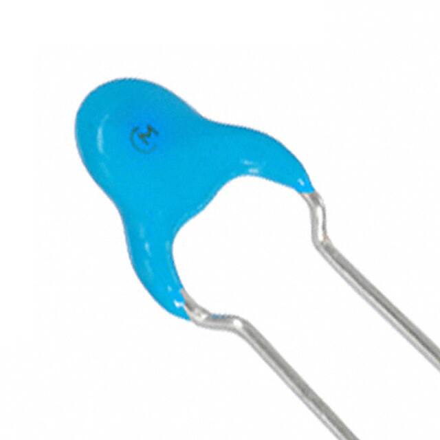
Lead Type Disc Ceramic Capacitors of Class 2 for General Purpose
Product specifications in this catalog are as of Dec. 2017, and are subject to change or
obsolescence without notice.
Please consult the approval sheet before ordering.Please read rating and Cautions first.
�Reference only
CAUTION
1. OPERATING VOLTAGE
When DC-rated capacitors are to be used in AC or ripple current circuits, be sure to maintain the Vp-p
value of the applied voltage or the Vo-p which contains DC bias within the rated voltage range.
When the voltage is started to apply to the circuit or it is stopped applying, the irregular voltage may
be generated for a transit period because of resonance or switching. Be sure to use a capacitor
within rated voltage containing these irregular voltage.
When DC-rated capacitors are to be used in input circuits from commercial power source (AC filter),
be sure to use Safety Recognized Capacitors because various regulations on withstand voltage
or impulse withstand established for each equipment should be taken into considerations.
Voltage
Positional
Measurement
DC Voltage
Vo-p
DC+AC Voltage
Vo-p
AC Voltage
Vp-p
Pulse Voltage(1) Pulse Voltage(2)
Vp-p
Vp-p
2. OPERATING TEMPERATURE AND SELF-GENERATED HEAT
Keep the surface temperature of a capacitor below the upper limit of its rated operating temperature
range. Be sure to take into account the heat generated by the capacitor itself.
When the capacitor is used in a high-frequency current, pulse current or the like, it may have the selfgenerated heat due to dielectric-loss. The allowable frequency should be in less than 300kHz in sine
wave. Applied voltage should be the load such as self-generated heat is within 20 C on the condition of
atmosphere temperature 25 C. When measuring, use a thermocouple of small thermal capacity-K of
0.1mm and be in the condition where capacitor is not affected by radiant heat of other components and
wind of surroundings. While, in case of non-sine wave which include a harmonic frequency, please
contact our sales representatives or product engineers.
3. FAIL-SAFE
When capacitor would be broken, failure may result in a short circuit. Be sure to provide an appropriate
fail-safe function like a fuse on your product if failure would follow an electric shock, fire or fume.
4. VIBRATION AND IMPACT
Do not expose a capacitor or its leads to excessive shock or vibration during use.
5. SOLDERING
When soldering this product to a PCB/PWB, do not exceed the solder heat resistance specification of the
capacitor. Subjecting this product to excessive heating could melt the internal junction solder and may
result in thermal shocks that can crack the ceramic element.
When soldering capacitor with a soldering iron, it should be performed in following conditions.
Temperature of iron tip : 400 C max.
Soldering iron wattage : 50W max.
Soldering time
: 3.5 s max.
EGD06F
1 / 21
�Reference only
6. BONDING, RESIN MOLDING AND COATING
In case of bonding, molding or coating this product, verify that these processes do not affect the
quality of capacitor by testing the performance of the bonded, molded or coated product in the
intended equipment.
In case of the amount of applications, dryness / hardening conditions of adhesives and molding
resins containing organic solvents (ethyl acetate, methyl ethyl ketone, toluene, etc.) are unsuitable,
the outer coating resin of a capacitor is damaged by the organic solvents and it may result, worst
case, in a short circuit.
The variation in thickness of adhesive, molding resin or coating may cause a outer coating resin
cracking and/or ceramic element cracking of a capacitor in a temperature cycling.
7. TREATMENT AFTER BONDING, RESIN MOLDING AND COATING
When the outer coating is hot (over 100 ℃) after soldering, it becomes soft and fragile.
So please be careful not to give it mechanical stress.
Failure to follow the above cautions may result, worst case, in a short circuit and cause fuming or partial
dispersion when the product is used.
8. OPERATING AND STORAGE ENVIRONMENT
The insulating coating of capacitors does not form a perfect seal; therefore, do not use or store
capacitors
in a corrosive atmosphere, especially where chloride gas, sulfide gas, acid, alkali, salt or the like are
present. And avoid exposure to moisture. Before cleaning, bonding, or molding this product, verify that
these processes do not affect product quality by testing the performance of a cleaned, bonded or molded
product in the intended equipment. Store the capacitors where the temperature and relative humidity do
not exceed -10 to 40 C and 15 to 85%. Use capacitors within 6 months after delivered.
Check the solderability after 6 months or more.
9. LIMITATION OF APPLICATIONS
Please contact us before using our products for the applications listed below which require especially
high reliability for the prevention of defects which might directly cause damage to the third party’s life,
body or property.
1. Aircraft equipment
2. Aerospace equipment
3. Undersea equipment
4. Power plant control equipment
5. Medical equipment
6. Transportation equipment (vehicles, trains, ships, etc.)
7. Traffic signal equipment
8. Disaster prevention / crime prevention equipment
9. Data-processing equipment exerting influence on public
10. Application of similar complexity and/or reliability requirements to the applications listed
in the above.
EGD06F
2 / 21
�Reference only
NOTICE
1. CLEANING (ULTRASONIC CLEANING)
To perform ultrasonic cleaning, observe the following conditions.
Rinse bath capacity : Output of 20 watts per liter or less.
Rinsing time : 5 min maximum.
Do not vibrate the PCB/PWB directly.
Excessive ultrasonic cleaning may lead to fatigue destruction of the lead wires.
2. CAPACITANCE CHANGE OF CAPACITORS
- Class 1 capacitors
Capacitance might change a little depending on a surrounding temperature or an applied voltage.
Please contact us if you use for the strict time constant circuit.
- Class 2 and 3 capacitors
Class 2 and 3 capacitors like temperature characteristic B, E and F have an aging characteristic,
whereby the capacitor continually decreases its capacitance slightly if the capacitor leaves for a
long time. Moreover, capacitance might change greatly depending on a surrounding temperature or
an applied voltage. So, it is not likely to be able to use for the time constant circuit.
Please contact us if you need a detail information.
NOTE
1.Please make sure that your product has been evaluated in view of your specifications with our
product being mounted to your product.
2.You are requested not to use our product deviating from this specification.
EGD06F
3 / 21
�Reference only
1. Application
This specification is applied to Lead Type Disc Ceramic Capacitors of DC2kV ~3.15kV ratings and
Class 2 of DEB series used for General Electric equipment.
Do not use these products in any automotive power train or safety equipment including battery chargers
for electric vehicles and plug-in hybrids.
2. Rating
2-1. Operating temperature range
-25
+85C
2-2. Part number configuration
ex.) DEB
Series
B3
Temperature
characteristic
3D
Rated
voltage
332
K
A3
B
Capacitance Capacitance Lead
Packing
tolerance
code style code
.
Individual
specification
Temperature characteristic
Code
Temperature characteristic
B3
B
E3
E
F3
F
Please confirm detailed specification on Specification and test methods .
Rated voltage
Code
3D
3F
Rated voltage
DC2kV
DC3.15kV
Capacitance
The first two digits denote significant figures ; the last digit denotes the multiplier of 10 in pF.
ex.) In case of 332.
33102 = 3300pF
Capacitance tolerance
Please refer to Part number list .
Lead code
Code
Lead style
Vertical crimp long type
A
Straight long type
C
Vertical crimp short type
B
Straight short type
D
Vertical crimp taping type
N
Straight taping type
P
Please refer to Part number list .
Solder coated copper wire is applied for termination.
4 / 21
�Reference only
Packing style code
Code
B
A
Packing type
Bulk type
Ammo pack taping type
Individual specification
In case part number cannot be identified without ‘individual specification’ , it is added at
the end of part number.
3. Marking
Temperature characteristic : Letter code
Identified by code for char. B or char. E.
(Omitted for maximum body diameter 9mm and under )
Nominal capacitance
: 3 digit system
Capacitance tolerance
: Code(Omitted for maximum body diameter 6mm and under)
Rated voltage
: Letter code(In case of DC3.15kV, marked with 3KV)
Company name code
: Abbreviation
(Omitted for maximum body diameter 9mm and under)
Manufacturing year
: Letter code(The last digit of A.D. year.)
(Omitted for maximum body diameter 5mm and under)
Manufacturing month
: Code(Omitted for maximum body diameter 5mm and under)
Feb./Mar. 2
Aug./Sep. 8
Apr./May 4
Oct./Nov. O
Jun./Jul. 6
Dec./Jan. D
(Example)
B
332K
2KV
5 / 21
�Reference only
4. Part number list
Unit : mm
T.C.
Cap.
Cap.
(pF)
tol.
Customer Part Number
Murata Part Number
Dimension (mm)
DC
Rated Volt.
(V)
D
T
F
d
Lead
Code
Pack
qty.
(pcs)
B
100
±10%
DEBB33D101KC1B
2000
4.5
5.0
5.0
0.5
C1
500
B
150
±10%
DEBB33D151KC1B
2000
4.5
5.0
5.0
0.5
C1
500
B
220
±10%
DEBB33D221KC1B
2000
4.5
5.0
5.0
0.5
C1
500
B
330
±10%
DEBB33D331KC1B
2000
5.0
5.0
5.0
0.5
C1
500
B
470
±10%
DEBB33D471KA2B
2000
6.0
5.0
5.0
0.6
A2
500
B
680
±10%
DEBB33D681KA2B
2000
7.0
5.0
5.0
0.6
A2
500
B
1000
±10%
DEBB33D102KA2B
2000
8.0
5.0
5.0
0.6
A2
250
B
1500
±10%
DEBB33D152KA2B
2000
9.0
5.0
5.0
0.6
A2
250
B
2200
±10%
DEBB33D222KA2B
2000
10.0
5.0
5.0
0.6
A2
250
B
3300
±10%
DEBB33D332KA3B
2000
12.0
5.0
7.5
0.6
A3
200
B
4700
±10%
DEBB33D472KA3B
2000
15.0
5.0
7.5
0.6
A3
100
B
100
±10%
DEBB33F101KCDB
3150
5.0
6.0
7.5
0.5
CD
500
B
150
±10%
DEBB33F151KCDB
3150
5.0
6.0
7.5
0.5
CD
500
B
220
±10%
DEBB33F221KCDB
3150
5.0
6.0
7.5
0.5
CD
500
B
330
±10%
DEBB33F331KC3B
3150
6.0
6.0
7.5
0.6
C3
500
B
470
±10%
DEBB33F471KC3B
3150
7.0
6.0
7.5
0.6
C3
250
B
680
±10%
DEBB33F681KA3B
3150
8.0
6.0
7.5
0.6
A3
250
B
1000
±10%
DEBB33F102KA3B
3150
9.0
6.0
7.5
0.6
A3
250
B
1500
±10%
DEBB33F152KA3B
3150
11.0
6.0
7.5
0.6
A3
250
B
2200
±10%
DEBB33F222KA3B
3150
13.0
6.0
7.5
0.6
A3
200
B
3300
±10%
DEBB33F332KA3B
3150
15.0
6.0
7.5
0.6
A3
100
E
1000 +80/-20%
DEBE33D102ZA2B
2000
6.0
5.0
5.0
0.6
A2
500
E
2200 +80/-20%
DEBE33D222ZA2B
2000
8.0
5.0
5.0
0.6
A2
250
E
4700 +80/-20%
DEBE33D472ZA2B
2000
11.0
5.0
5.0
0.6
A2
250
E
10000 +80/-20%
DEBE33D103ZA3B
2000
16.0
5.0
7.5
0.6
A3
100
E
1000 +80/-20%
DEBE33F102ZC3B
3150
7.0
6.0
7.5
0.6
C3
250
E
2200 +80/-20%
DEBE33F222ZA3B
3150
10.0
6.0
7.5
0.6
A3
250
6 / 21
�Reference only
Unit : mm
T.C.
Cap.
Cap.
(pF)
tol.
Customer Part Number
Murata Part Number
Dimension (mm)
DC
Rated Volt.
(V)
D
T
F
d
Lead
Code
Pack
qty.
(pcs)
E
4700 +80/-20%
DEBE33F472ZA3B
3150
13.0
6.0
7.5
0.6
A3
200
F
1000 +80/-20%
DEBF33D102ZC1B
2000
5.0
5.0
5.0
0.5
C1
500
F
2200 +80/-20%
DEBF33D222ZA2B
2000
7.0
5.0
5.0
0.6
A2
500
F
4700 +80/-20%
DEBF33D472ZA2B
2000
9.0
5.0
5.0
0.6
A2
250
F
10000 +80/-20%
DEBF33D103ZA3B
2000
12.0
5.0
7.5
0.6
A3
200
7 / 21
�Reference only
Unit : mm
T.C.
Cap.
Cap.
(pF)
tol.
Customer Part Number
Murata Part Number
Dimension (mm)
DC
Rated Volt.
(V)
D
T
F
d
Lead
Code
Pack
qty.
(pcs)
B
100
±10%
DEBB33D101KD1B
2000
4.5
5.0
5.0
0.5
D1
500
B
150
±10%
DEBB33D151KD1B
2000
4.5
5.0
5.0
0.5
D1
500
B
220
±10%
DEBB33D221KD1B
2000
4.5
5.0
5.0
0.5
D1
500
B
330
±10%
DEBB33D331KD1B
2000
5.0
5.0
5.0
0.5
D1
500
B
470
±10%
DEBB33D471KB2B
2000
6.0
5.0
5.0
0.6
B2
500
B
680
±10%
DEBB33D681KB2B
2000
7.0
5.0
5.0
0.6
B2
500
B
1000
±10%
DEBB33D102KB2B
2000
8.0
5.0
5.0
0.6
B2
500
B
1500
±10%
DEBB33D152KB2B
2000
9.0
5.0
5.0
0.6
B2
500
B
2200
±10%
DEBB33D222KB2B
2000
10.0
5.0
5.0
0.6
B2
500
B
3300
±10%
DEBB33D332KB3B
2000
12.0
5.0
7.5
0.6
B3
250
B
4700
±10%
DEBB33D472KB3B
2000
15.0
5.0
7.5
0.6
B3
200
B
100
±10%
DEBB33F101KDDB
3150
5.0
6.0
7.5
0.5
DD
500
B
150
±10%
DEBB33F151KDDB
3150
5.0
6.0
7.5
0.5
DD
500
B
220
±10%
DEBB33F221KDDB
3150
5.0
6.0
7.5
0.5
DD
500
B
330
±10%
DEBB33F331KD3B
3150
6.0
6.0
7.5
0.6
D3
500
B
470
±10%
DEBB33F471KD3B
3150
7.0
6.0
7.5
0.6
D3
500
B
680
±10%
DEBB33F681KB3B
3150
8.0
6.0
7.5
0.6
B3
500
B
1000
±10%
DEBB33F102KB3B
3150
9.0
6.0
7.5
0.6
B3
500
B
1500
±10%
DEBB33F152KB3B
3150
11.0
6.0
7.5
0.6
B3
500
B
2200
±10%
DEBB33F222KB3B
3150
13.0
6.0
7.5
0.6
B3
250
B
3300
±10%
DEBB33F332KB3B
3150
15.0
6.0
7.5
0.6
B3
200
E
1000 +80/-20%
DEBE33D102ZB2B
2000
6.0
5.0
5.0
0.6
B2
500
E
2200 +80/-20%
DEBE33D222ZB2B
2000
8.0
5.0
5.0
0.6
B2
500
E
4700 +80/-20%
DEBE33D472ZB2B
2000
11.0
5.0
5.0
0.6
B2
500
E
10000 +80/-20%
DEBE33D103ZB3B
2000
16.0
5.0
7.5
0.6
B3
200
E
1000 +80/-20%
DEBE33F102ZD3B
3150
7.0
6.0
7.5
0.6
D3
500
E
2200 +80/-20%
DEBE33F222ZB3B
3150
10.0
6.0
7.5
0.6
B3
500
8 / 21
�Reference only
Unit : mm
T.C.
Cap.
Cap.
(pF)
tol.
Customer Part Number
Murata Part Number
Dimension (mm)
DC
Rated Volt.
(V)
D
T
F
d
Lead
Code
Pack
qty.
(pcs)
E
4700 +80/-20%
DEBE33F472ZB3B
3150
13.0
6.0
7.5
0.6
B3
250
F
1000 +80/-20%
DEBF33D102ZD1B
2000
5.0
5.0
5.0
0.5
D1
500
F
2200 +80/-20%
DEBF33D222ZB2B
2000
7.0
5.0
5.0
0.6
B2
500
F
4700 +80/-20%
DEBF33D472ZB2B
2000
9.0
5.0
5.0
0.6
B2
500
F
10000 +80/-20%
DEBF33D103ZB3B
2000
12.0
5.0
7.5
0.6
B3
250
9 / 21
�Reference only
Unit : mm
T.C.
Cap.
(pF)
Cap.
tol.
Customer Part Number
Murata Part Number
Dimension (mm)
DC
Rated volt.
(V)
D
T
F
d
P
Lead
code
Pack
qty.
(pcs)
B
100
±10%
DEBB33D101KP2A
2000
4.5
5.0
5.0
0.6 12.7
P2
1500
B
150
±10%
DEBB33D151KP2A
2000
4.5
5.0
5.0
0.6 12.7
P2
1500
B
220
±10%
DEBB33D221KP2A
2000
4.5
5.0
5.0
0.6 12.7
P2
1500
B
330
±10%
DEBB33D331KP2A
2000
5.0
5.0
5.0
0.6 12.7
P2
1500
B
470
±10%
DEBB33D471KN2A
2000
6.0
5.0
5.0
0.6 12.7
N2
1500
B
680
±10%
DEBB33D681KN2A
2000
7.0
5.0
5.0
0.6 12.7
N2
1500
B
1000
±10%
DEBB33D102KN2A
2000
8.0
5.0
5.0
0.6 12.7
N2
1500
B
1500
±10%
DEBB33D152KN2A
2000
9.0
5.0
5.0
0.6 12.7
N2
1500
B
2200
±10%
DEBB33D222KN2A
2000
10.0
5.0
5.0
0.6 12.7
N2
1500
B
3300
±10%
DEBB33D332KN3A
2000
12.0
5.0
7.5
0.6 15.0
N3
900
B
4700
±10%
DEBB33D472KN7A
2000
15.0
5.0
7.5
0.6 30.0
N7
500
B
100
±10%
DEBB33F101KP3A
3150
5.0
6.0
7.5
0.6 15.0
P3
900
B
150
±10%
DEBB33F151KP3A
3150
5.0
6.0
7.5
0.6 15.0
P3
900
B
220
±10%
DEBB33F221KP3A
3150
5.0
6.0
7.5
0.6 15.0
P3
900
B
330
±10%
DEBB33F331KP3A
3150
6.0
6.0
7.5
0.6 15.0
P3
900
B
470
±10%
DEBB33F471KP3A
3150
7.0
6.0
7.5
0.6 15.0
P3
900
B
680
±10%
DEBB33F681KN3A
3150
8.0
6.0
7.5
0.6 15.0
N3
900
B
1000
±10%
DEBB33F102KN3A
3150
9.0
6.0
7.5
0.6 15.0
N3
900
B
1500
±10%
DEBB33F152KN3A
3150
11.0
6.0
7.5
0.6 15.0
N3
900
B
2200
±10%
DEBB33F222KN3A
3150
13.0
6.0
7.5
0.6 15.0
N3
900
B
3300
±10%
DEBB33F332KN7A
3150
15.0
6.0
7.5
0.6 30.0
N7
500
E
1000 +80/-20%
DEBE33D102ZN2A
2000
6.0
5.0
5.0
0.6 12.7
N2
1500
E
2200 +80/-20%
DEBE33D222ZN2A
2000
8.0
5.0
5.0
0.6 12.7
N2
1500
E
4700 +80/-20%
DEBE33D472ZN2A
2000
11.0
5.0
5.0
0.6 12.7
N2
1500
E
10000 +80/-20%
DEBE33D103ZN7A
2000
16.0
5.0
7.5
0.6 30.0
N7
500
E
1000 +80/-20%
DEBE33F102ZP3A
3150
7.0
6.0
7.5
0.6 15.0
P3
900
E
2200 +80/-20%
DEBE33F222ZN3A
3150
10.0
6.0
7.5
0.6 15.0
N3
900
10 / 21
�Reference only
Unit : mm
T.C.
Cap.
(pF)
Cap.
tol.
Customer Part Number
Murata Part Number
Dimension (mm)
DC
Rated volt.
(V)
D
T
F
d
P
Lead
code
Pack
qty.
(pcs)
E
4700 +80/-20%
DEBE33F472ZN3A
3150
13.0
6.0
7.5
0.6 15.0
N3
900
F
1000 +80/-20%
DEBF33D102ZP2A
2000
5.0
5.0
5.0
0.6 12.7
P2
1500
F
2200 +80/-20%
DEBF33D222ZN2A
2000
7.0
5.0
5.0
0.6 12.7
N2
1500
F
4700 +80/-20%
DEBF33D472ZN2A
2000
9.0
5.0
5.0
0.6 12.7
N2
1500
F
10000 +80/-20%
DEBF33D103ZN3A
2000
12.0
5.0
7.5
0.6 15.0
N3
900
11 / 21
�Reference only
5. Specification and test methods
No.
Item
1
Appearance and dimensions
2
3
4
Marking
Dielectric
strength
Between lead
wires
Body
insulation
No failure.
Between lead
wires
10 000M min.
5
Insulation
Resistance (I.R.)
Capacitance
6
Dissipation Factor (D.F.)
7
Temperature characteristic
8
Strength of lead
Specification
No marked defect on appearance
form and dimensions.
Please refer to [Part number list].
To be easily legible.
No failure.
Within specified tolerance.
Pull
Test method
The capacitor should be inspected by naked eyes
for visible evidence of defect.
Dimensions should be measured with slide calipers.
The capacitor should be inspected by naked eyes.
The capacitor should not be damaged when DC
voltage of 200% of the rated voltage are applied
between the lead wires for 1 to 5 s.
(Charge/Discharge current50mA.)
The capacitor is placed in the container with metal
balls of diameter 1mm so that each lead wire,
shortcircuited, is kept about 2mm
off the balls as shown
in the figure, and DC
voltage of 1.3kV is
applied for 1 to 5 s
About 2mm
between capacitor lead
Metal balls
wires and small metals.
(Charge/Discharge current50mA.)
The insulation resistance should be measured with
DC50050V within 605 s of charging.
The capacitance should be measured at 20C with
10.2kHz and AC5V(r.m.s.) max..
The dissipation factor should be measured at 20C
with 10.2kHz and AC5V(r.m.s.) max..
The capacitance measurement should be made at
each step specified in Table.
Char. B,E : 2.5% max.
Char. F : 5.0% max.
Char. B : Within 10%
Char. E : Within +20/-55%
Char. F : Within +30/-80%
Pre-treatment : Capacitor should be stored at 852C for 1 h, then placed at *room
condition for 242 h before initial measurements.
Step
1
2
3
4
5
Temp.(C)
202
-253
202
852
202
Lead wire should not cut off.
Capacitor should not be broken.
As shown in the figure at right, fix the
body of the capacitor and apply a tensile
weight gradually to each lead wire in the
radial direction of the capacitor up to
10N ( 5N for lead diameter 0.5mm ),
and keep it for 101 s.
Bending
Each lead wire should be subjected to 5N ( 2.5N for
lead diameter 0.5mm ) of weight and bent 90 at the
point of egress, in one direction, then returned to its
original position, and bent 90 in the opposite
direction at the rate of one bend in 2 to 3 s.
9
Vibration
Appearance
No marked defect.
The capacitor should be firmly soldered to the
resistance
supporting lead wire and vibrated at a frequency
Capacitance
Within specified tolerance.
range of 10 to 55Hz, 1.5mm in total amplitude, with
D.F.
Char. B,E : 2.5% max.
about a 1min rate of vibration change from 10Hz
Char. F : 5.0% max.
to 55Hz and back to 10Hz. Apply for a total of 6 h;
2 h each in 3 mutually perpendicular directions.
10 Solderability of leads
Lead wire should be soldered
The lead wire of a capacitor should be dipped into a
with uniformly coated on the axial ethanol solution of 25wt% rosin and then into
direction over 3/4 of the
molten solder for 20.5 s. In both cases the depth of
circumferential direction.
dipping is up to about 1.5 to 2mm from the root of
lead wires.
Temp. of solder :
245±5°C Lead Free Solder (Sn-3Ag-0.5Cu)
235±5°C H63 Eutectic Solder
* "room condition" Temperature: 15 to 35C, Relative humidity: 45 to 75%, Atmospheric pressure: 86 to 106kPa
ESDEB01A
12 / 21
�Reference only
No.
11
Item
Soldering effect
Appearance
(Non-preheat)
Capacitance
change
Dielectric
strength
(Between
lead wires)
12
Soldering effect
(On-preheat)
Appearance
Capacitance
change
Dielectric
strength
(Between
lead wires)
Specification
No marked defect.
Char. B : Within 5%
Char. E : Within 15%
Char. F : Within 20%
Per item 3.
No marked defect.
Char. B : Within 5%
Char. E : Within 15%
Char. F : Within 20%
Per item 3.
Test method
The lead wire should be immersed into the melted
solder of 35010C ( Body of 5 and under:
2705C ) up to about 1.5 to 2.0mm from the
main body for 3.50.5 s. ( Body of 5 and under:
50.5 s. )
Pre-treatment : Capacitor should be stored at
852C for 1 h, then placed at
* room condition for 242 h
before initial measurements.
Post-treatment : Capacitor should be stored for
4 to 24 h at * room condition.
First the capacitor should be stored at
120+0/-5°C for 60+0/-5 s.
Then, as in figure, the lead wires should be
immersed solder of 260+0/-5°C up to 1.5 to
2.0mm from the root of terminal for 7.5+0/-1 s.
Pre-treatment : Capacitor should be stored at
852C for 1 h, then placed at
* room condition for 242 h
before initial measurements.
Post-treatment : Capacitor should be stored for
4 to 24 h at * room condition.
13
Humidity
Appearance
No marked defect.
Set the capacitor for 500 +24/-0 h at 402C in
(Under steady
Capacitance
Char. B : Within 10%
90 to 95% relative humidity.
state)
change
Pre-treatment : Capacitor should be stored at
Char. E : Within 20%
852C for 1 h, then placed at
Char. F : Within 30%
D.F.
Char. B,E : 5.0% max.
* room condition for 242 h
Char. F : 7.5% max.
before initial measurements.
Post-treatment : Capacitor should be stored for 1
I.R.
1 000M min.
to 2 h at * room condition.
14
Humidity loading
Appearance
No marked defect.
Apply the rated voltage for 500 +24/-0 h at
Capacitance
402C in 90 to 95% relative humidity.
Char. B : Within 10%
change
(Charge/Discharge current50mA.)
Char. E : Within 20%
Pre-treatment : Capacitor should be stored at
Char. F : Within 30%
852C for 1 h, then placed at
D.F.
Char. B,E : 5.0% max.
* room condition for 242 h
Char. F : 7.5% max.
before initial measurements.
I.R.
500M min.
Post-treatment : Capacitor should be stored at
852C for 1 h, then placed at
* room condition for 242 h.
15
Life
Appearance
No marked defect.
Apply a DC voltage of 150% of the rated voltage
Capacitance
for 1 000 +48/-0 h at 852C, and relative
Char. B : Within 10%
change
humidity of 50% max..
Char. E : Within 20%
(Charge/Discharge current50mA.)
Char. F : Within 30%
Pre-treatment : Capacitor should be stored at
D.F.
Char. B,E : 4.0% max.
852C for 1 h, then placed at
Char. F : 7.5% max.
* room condition for 242 h
I.R.
2 000M min.
before initial measurements.
Post-treatment : Capacitor should be stored at
852C for 1 h, then placed at
* room condition for 242 h.
* "room condition" Temperature: 15 to 35C, Relative humidity: 45 to 75%, Atmospheric pressure: 86 to 106kPa
ESDEB01A
13 / 21
�Reference only
No.
16
Item
Temperature and
Appearance
Immersion cycle
Capacitance
change
D.F.
I.R.
Dielectric
strength
(Between
lead wires)
Specification
No marked defect.
Char. B : Within 10%
Char. E : Within 20%
Char. F : Within 30%
Char. B,E : 4.0% max.
Char. F : 7.5% max.
2 000M min.
Per item 3.
Test method
The capacitor should be subjected to
5 temperature cycles, then consecutively to
2 immersion cycles.
Step
1
2
3
4
Temperature(C)
-253
Room Temp.
+853
Room Temp.
Time
30 min
3 min
30 min
3 min
Cycle time : 5 cycle
Step
Temperature(C)
Time
1
+65+5/-0
15 min
2
03
15 min
Immersion
water
Clean
water
Salt
water
Cycle time : 2 cycle
Pre-treatment : Capacitor should be stored at
852C for 1 h, then placed at
* room condition for 242 h
before initial measurements.
Post-treatment : Capacitor should be stored for
4 to 24 h at * room condition.
* "room condition" Temperature: 15 to 35C, Relative humidity: 45 to 75%, Atmospheric pressure: 86 to 106kPa
ESDEB01A
14 / 21
�Reference only
6.Packing specification
Bulk type (Packing style code : B)
1
2
The number of packing = Packing quantity n
The size of packing case and packing way
1 : Please refer to [Part number list].
2 : Standard n = 20 (bag)
Polyethylene bag
Partition
270 max.
125 max.
340 max.
Note)
The outer package and the number of
outer packing be changed by the order
getting amount.
Unit : mm
Ammo pack taping type (Packing style code : A)
The tape with capacitors is packed zigzag into a case.
When body of the capacitor is piled on other body under it.
There should be 3 pitches and over without capacitors in leader and trailer.
The size of packing case and packing way
240 max.
Position of label
340 max.
60 max.
Capacitor
Hold down tape
Base tape
Hold down
tape upper
EKBCDE01
15 / 21
Unit : mm
�Reference only
7. Taping specification
7-1. Dimension of capacitors on tape
Vertical crimp taping type < Lead code : N2 >
Pitch of component 12.7mm / Lead spacing 5.0mm
Unit : mm
Item
Code
Dimensions
Remarks
Pitch of component
P
12.71.0
Pitch of sprocket hole
P0
12.70.3
Lead spacing
F
5.00.2
Length from hole center to component center
P2
6.351.3
Length from hole center to lead
P1
3.850.7
Body diameter
D
Please refer to [Part number list ].
Deviation along tape, left or right
S
01.0
Carrier tape width
W
18.00.5
Position of sprocket hole
W1
9.00.5
H0
18.0 2.0
0
Diameter of sprocket hole
D0
4.00.1
Lead diameter
d
0.600.05
Total tape thickness
t1
0.60.3
Total thickness, tape and lead wire
t2
1.5 max.
Deviation across tape, front
h1
Deviation across tape, rear
h2
Portion to cut in case of defect
L
11.0 1.0
Hold down tape width
W0
11.5 min.
Hold down tape position
W2
1.51.5
Coating extension on lead
e
Up to the end of crimp
Body thickness
T
Please refer to [Part number list ].
Lead distance between reference and bottom
planes
0.8
Deviation of progress direction
They include deviation by lead bend .
Deviation of tape width direction
0.51.0
Protrusion length
They include hold down tape thickness.
1.0 max.
0
ETP1N201A
16 / 21
�Reference only
Vertical crimp taping type < Lead code : N3 >
Pitch of component 15.0mm / Lead spacing 7.5mm
Unit : mm
Item
Code
Dimensions
Remarks
Pitch of component
P
15.02.0
Pitch of sprocket hole
P0
15.00.3
Lead spacing
F
7.51.0
Length from hole center to component center
P2
7.51.5
Length from hole center to lead
P1
3.751.0
Body diameter
D
Please refer to [ Part number list ].
Deviation along tape, left or right
S
02.0
Carrier tape width
W
18.00.5
Position of sprocket hole
W1
9.00.5
H0
18.02.0
0
Lead distance between reference and bottom
planes
Deviation of progress direction
They include deviation by lead bend .
Deviation of tape width direction
0.51.0
Protrusion length
Diameter of sprocket hole
D0
4.00.1
Lead diameter
d
0.600.05
Total tape thickness
t1
0.60.3
Total thickness, tape and lead wire
t2
1.5 max.
Deviation across tape, front
h1
Deviation across tape, rear
h2
Portion to cut in case of defect
L
11.0 1.0
Hold down tape width
W0
11.5 min.
Hold down tape position
W2
1.51.5
Coating extension on lead
e
Up to the end of crimp
Body thickness
T
Please refer to [ Part number list ].
They include hold down tape thickness.
2.0 max.
0
ETP1N30101A
17 / 21
�Reference only
Vertical crimp taping type < Lead code : N7 >
Pitch of component 30.0mm /Lead spacing 7.5mm
Unit : mm
Item
Code
Dimensions
Remarks
Pitch of component
P
30.02.0
Pitch of sprocket hole
P0
15.00.3
Lead spacing
F
7.51.0
Length from hole center to component center
P2
7.51.5
Length from hole center to lead
P1
3.751.0
Body diameter
D
Please refer to [ Part number list ].
Deviation along tape, left or right
S
02.0
Carrier tape width
W
18.00.5
Position of sprocket hole
W1
9.00.5
H0
18.02.0
0
Lead distance between reference and bottom
planes
Deviation of progress direction
They include deviation by lead bend.
Deviation of tape width direction
0.51.0
Protrusion length
Diameter of sprocket hole
D0
4.00.1
Lead diameter
d
0.600.05
Total tape thickness
t1
0.60.3
Total thickness, tape and lead wire
t2
1.5 max.
Deviation across tape, front
h1
Deviation across tape, rear
h2
Portion to cut in case of defect
L
11.0 1.0
Hold down tape width
W0
11.5 min.
Hold down tape position
W2
1.51.5
Coating extension on lead
e
Up to the end of crimp
Body thickness
T
Please refer to [ Part number list ].
They include hold down tape thickness.
2.0 max.
0
ETP1N70101A
18 / 21
�Reference only
Straight taping type < Lead code: P2 >
Pitch of component 12.7mm / Lead spacing 5.0mm
Unit : mm
Item
Code
Dimensions
Remarks
Pitch of component
P
12.71.0
Pitch of sprocket hole
P0
12.70.3
Lead spacing
F
5.00.2
Length from hole center to component center
P2
6.351.3
Length from hole center to lead
P1
3.850.7
Body diameter
D
Please refer to [ Part number list ].
Deviation along tape, left or right
S
01.0
Carrier tape width
W
18.00.5
Position of sprocket hole
W1
9.00.5
H
20.01.5
1.0
Lead distance between reference and bottom
planes
0.8
Deviation of progress direction
They include deviation by lead bend .
Deviation of tape width direction
0.51.0
Protrusion length
Diameter of sprocket hole
D0
4.00.1
Lead diameter
d
0.600.05
Total tape thickness
t1
0.60.3
Total thickness, tape and lead wire
t2
1.5 max.
Deviation across tape, front
h1
Deviation across tape, rear
h2
Portion to cut in case of defect
L
11.0 1.0
Hold down tape width
W0
11.5 min.
Hold down tape position
W2
1.51.5
Coating extension on lead
e
3.0 max.
Body thickness
T
Please refer to [ Part number list ].
They include hold down tape thickness.
1.0 max.
0
ETP1P20101A
19 / 21
�Reference only
Straight taping type < Lead code : P3 >
Pitch of component 15.0mm / Lead spacing 7.5mm
Unit : mm
Item
Code
Dimensions
Remarks
Pitch of component
P
15.02.0
Pitch of sprocket hole
P0
15.00.3
Lead spacing
F
7.51.0
Length from hole center to component center
P2
7.51.5
Length from hole center to lead
P1
3.751.0
Body diameter
D
Please refer to [ Part number list ].
Deviation along tape, left or right
S
02.0
Carrier tape width
W
18.00.5
Position of sprocket hole
W1
9.00.5
H
20.01.5
1.0
Lead distance between reference and bottom
planes
Deviation of progress direction
They include deviation by lead bend .
Deviation of tape width direction
0.51.0
Protrusion length
Diameter of sprocket hole
D0
4.00.1
Lead diameter
d
0.600.05
Total tape thickness
t1
0.60.3
Total thickness, tape and lead wire
t2
1.5 max.
Deviation across tape, front
h1
Deviation across tape, rear
h2
Portion to cut in case of defect
L
11.0 1.0
Hold down tape width
W0
11.5 min.
Hold down tape position
W2
1.51.5
Coating extension on lead
e
3.0 max.
Body thickness
T
Please refer to [ Part number list ].
They include hold down tape thickness.
2.0 max.
0
ETP1P30101A
20 / 21
�Reference only
7-2. Splicing way of tape
1) Adhesive force of tape is over 3N at test condition as below.
W
Hold down tape
Base tape
2) Splicing of tape
a) When base tape is spliced
Base tape should be spliced by cellophane tape.
(Total tape thickness should be less than 1.05mm.)
Progress direction
in production line
Hold down tape
Base tape
About 30 to 50
Cellophane tape
No lifting for the direction of
progressing
Unit : mm
b) When hold down tape is spliced
Hold down tape should be spliced with overlapping.
(Total tape thickness should be less than 1.05mm.)
ape are spliced
Base tape and adhesive tape should be spliced with splicing tape.
20 to 60
Hold down tape
Progress direction
in production line
Base tape
Unit : mm
c) When both tape are spliced
Base tape and hold down tape should be spliced with splicing tape.
3 ) Missing components
There should be no consecutive missing of more than three components.
The number of missing components should be not more than 0.5% of
total components that should be present in a Ammo pack.
ETP2D03
21 / 21
�Appendix
EU RoHS
This products of the following crresponds to EU RoHS.
RoHS
maximum concentration values tolerated by weight in homogeneous materials
・1000 ppm maximum Lead
・1000 ppm maximum Mercury
・100 ppm maximum Cadmium
・1000 ppm maximum Hexavalent chromium
・1000 ppm maximum Polybrominated biphenyls (PBB)
・1000 ppm maximum Polybrominated diphenyl ethers (PBDE)
�Mouser Electronics
Authorized Distributor
Click to View Pricing, Inventory, Delivery & Lifecycle Information:
Murata:
DEBE33F102ZC3B DEBE33D222ZA2B DEBB33D471KN2A DEBE33D102ZA2B DEBB33F221KR5A
DEBE33F222ZA3B DEBB33D471KA2B DEBB33F471KA3B DEBE33D103ZECB DEBE33D103ZA3B
DEBB33F152KA3B DEBB33D152KA2B DEBB33F681KA3B DEBB33D681KA2B DEBB33F102KA3B
DEBB33D102KA2B DEBB33D101KA1B DEBB33D102KB2B DEBB33F101KP3A DEBB33F102KN3A
DEBB33F471KP3A DEBE33D102ZN2A DEBE33D103ZA4B DEBB33F151KP3A DEBB33D101KC1B
DEBB33D331KC1B DEBB33D221KC1B DEBB33D151KC1B DEBF33D102ZC1B DEBB33D472KA4B
DEBB33D472KA3B DEBB33D331KN2A DEBB33F471KC3B DEBB33D221KP2A DEBB33D152KB2B
DEBB33D331KP2A DEBB33D151KP2A DEBF33D222ZN2A DEBF33D472ZN2A DEBE33D472ZN2A
DEBB33F331KC3B DEBB33D332KA3B DEBB33F332KA3B DEBE33D103ZN7A DEBB33D331KA1B
DEBE33D472ZA2B DEBE33F472ZA3B DEBB33F471KN3A DEBF33D103ZA2B DEBF33D103ZA3B
DEBB33F151KCDB DEBB33F101KCDB DEBF33D102ZA1B DEBB33D222KA2B DEBB33F222KA3B
DEBB33F221KCDB DEBB33D222KN2A DEBB33F222KN3A DEBF33D222ZA2B DEBB33D102KN2A
DEBF33D472ZA2B DEBB33D101KD1B DEBB33D101KP2A DEBB33D151KD1B DEBB33D221KD1B
DEBB33D331KD1B DEBB33D471KB2B DEBB33D472KN7A DEBB33D681KB2B DEBB33F101KDDB
DEBB33F102KB3B DEBB33F151KDDB DEBB33F152KB3B DEBB33F221KDDB DEBB33F221KP3A
DEBB33F331KD3B DEBB33F331KP3A DEBB33F332KB3B DEBB33F471KD3B DEBB33F681KB3B
DEBE33D102ZB2B DEBE33D103ZB3B DEBE33D222ZB2B DEBE33D222ZN2A DEBE33D472ZB2B
DEBE33F102ZD3B DEBE33F222ZB3B DEBE33F222ZN3A DEBE33F472ZN3A DEBF33D102ZD1B
DEBF33D103ZB3B DEBF33D103ZN3A DEBF33D222ZB2B DEBF33D472ZB2B DEBB33D152KN2A
DEBB33D222KB2B DEBB33D332KB3B DEBB33D332KN3A DEBB33D472KB3B DEBB33D681KN2A
�


 工商网监
湘ICP备2023018690号
工商网监
湘ICP备2023018690号
