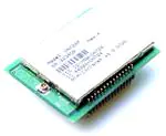
DNT24CA
DNT24PA
- 2.4 GHz Frequency Hopping Spread Spectrum Transceiver
- Point-to-point, Point-to-multipoint, Peer-to-peer and
Store & Forward Capabilities
- Transmitter RF Power Configurable - 6.3 or 63 mW
- Built-in Chip Antenna
- 250 kbps RF Data Rate
- Serial Port Data Rate up to 250 kbps, SPI Port Data Rate up to 500 kbps
- 128-Bit AES Encryption
- Separate Serial Port for Diagnostics
- Analog and Digital I/O for Sensor Applications
- FCC, Canadian IC and ETSI Certified for Unlicensed Operation
Low Cost
2.4 GHz FHSS
Transceiver
Modules with
I/O
The DNT24CA and DNT24PA FHSS transceiver modules provide a low-cost, versatile solution for wireless data communications in the 2.4 GHz ISM band. The RF output power can be
set at 6.3 or 63 mW. The modules include analog, digital and serial I/O, providing the
flexibility to serve applications ranging from cable replacements to sensor networks. The builtin chip antenna makes these modules very easy to integrate.
DNT24CA/PA Absolute Maximum Ratings
Value
Units
Power Supply Input
Rating
-0.5 to +6.5
V
All Input/Output Pins
-0.5 to +3.3
V
0
dBm
Input Power to RFIO Port
Non-Operating Ambient Temperature Range
-40 to +85
o
C
DNT24CA/PA Electrical Characteristics
Characteristic
Sym
Notes
Operating Frequency Range
Hop Duration
1
Number of RF Channels
1
Modulation
Minimum
Typical
Maximum
Units
2406
2475
MHz
8
100
ms
15 or 24
FSK
RF Data Transmission Rate
-5
Receiver Sensitivity @ 10 BER
Transmitter RF Output Power
Antenna
System Topologies
Access Scheme
Copyright © Murata Manufacturing Co., Ltd. All rights reserved. 2015
DNT24CA/PA (R) 01/31/19
1 of 7
1
250
kbps
-100
dBm
6.3 or 63 mW
Dielectric Chip Antenna
Point-to-Point, Point-to-Multipoint,
Peer-to-Peer and Store & Forward
Ad Hoc TDMA
www.murata.com
�DNT24CA/PA Electrical Characteristics
Characteristic
Sym
Notes
ADC Input Range
Minimum
Typical
0
ADC Input Resolution
ADC Sample Rate
Maximum
2.7
V
12
bits
100
Signal Source Impedance for ADC Reading
ADC External Reference Voltage Range
DAC Output Range
Hz
10
KΩ
1.0
2.7
V
0
3.3
V
12
bits
DAC Output Resolution
1.2, 2.4, 4.8, 9.6, 14.4, 19.2, 28.8,
38.4, 57.6, 115.2, 230.4, 250.0
Primary and Diagnostic Serial Port Baud Rates
Serial Peripheral Interface Data Rate
Units
kbps
125
500
kbps
Logic Low Input Level
-0.5
0.8
V
Logic High Input Level
2.45
3.3
V
Digital I/O:
Logic Input Internal Pull-up Resistor
20
+5.5
Vdc
Power Supply Voltage Ripple
10
mVP-P
Peak Transmit Mode Current, 63 mW Output
140
mA
Power Supply Voltage Range
+3.3
KΩ
VCC
Average Operating Receive Current:
Base and Remote, Continuous Data Stream
55
mA
Remote, Linked, No Data Transmission
15
mA
Sleep Current
2
3
DNT24CA Mounting
Reflow Soldering
DNT24PA Mounting
Socket
6
µA
Operating Temperature Range
-40
85
o
Operating Relative Humidity Range, Non-condensing
10
90
%
C
Notes:
1. The DNT24CA and DNT24PA achieve regulatory certification under FHSS rules.
2. Maximum sleep current occurs at +85 oC.
CAUTION: Electrostatic Sensitive Device. Observe precautions when handling.
Copyright © Murata Manufacturing Co., Ltd. All rights reserved. 2015
DNT24CA/PA (R) 01/31/19
2 of 7
www.murata.com
�T 2
C A /
T 2
P A B lo c k
ia g r a m
1
G
A C T (
/
C
2
IA G _ T X )
(
IR Q 0
G P IO 0
R A
IR Q 1 /
IO _ T X
R A
5
P W R
P L L _ L O C K
(/H O S T _ C T S )
8
A C 0
9
G P IO 2
1 0
G P IO 1
1 1
A V )
S
S
n S S _
I
T /R
T /R
F il e r
R F IO
O
A T A
n S S _ C O
1 2
A C 1
2 . G H z
T r a n s c e iv e r
S C K
M ic r o c o n r o lle r
G P IO 5 (/H O S T _ R T S )
G P IO 3 (
C L K
A T A
IO _ R X
G P IO
C h ip
A n e n n a
3
IA G _ R X )
P R E
F IG
1 3
V C C
1
1 5
G
+ 3 .3 V
R e g
2
2
2 8
R S V
3 0
C _ E X T _ R E F
C 1
C 0
/R E S E T
3 .3 V _ O U T
A
G
2 9
G
2 5
R S V
2
G
2 3
A
2 2
R S V
2 1
/S S
2 0
S C L K
1 9
M O S I
1 8
M IS O
1
A
1
Figure 1
DNT24CA/PA Hardware
DNT24CA/PA Firmware
The major components of these modules include a
2.4 GHz FHSS transceiver and a low current 8-bit
microcontroller. These modules operate in the 2.4
GHz ISM band. There are 12 selectable hopping patterns providing compatibility with frequency allocations
in most regions of the world. The modules also have
two selectable RF output power levels: 6.3 mW and 63
mW.
DNT24CA/PA firmware operates using hybrid Ad Hoc
TDMA channel access optimized for periodic burst
transmissions. DNT24CA/PA firmware operates “out
of the box” using point-to-point transparent serial
mode, with point-to-multipoint, peer-to-peer and store
& forward system topologies also supported.
The DNT24CA/PA provide a variety of hardware interfaces. There are two serial ports plus one SPI port. Either the primary serial port or the SPI port can be
selected for data communications. The second serial
port is dedicated to diagnostics. The primary and diagnostic serial ports support most standard baud rates
up to 250.0 kbps. The SPI port supports data rates up
to 500 kbps. These modules also include three ADC
inputs, two DAC outputs, and six general-purpose digital I/O ports. Four of the digital I/O ports support an
optional interrupt-from-sleep mode when configured
as inputs. The DNT24CA is designed for solder reflow
mounting. The DNT24PA is designed for plug-in connector mounting.
The firmware provides the user with a rich set of configuration options including a choice of hopping patterns, hopping dwell times, serial and/or SPI data port
operation, serial and SPI data rate selection, RF output power selection, plus configurable analog and digital I/O lines.
Data integrity is protected by 24-bit error detection,
with optional ACK and automatic transmission retries
or redundant transmissions. 128-bit AES encryption
provides a high level of data security for sensitive
applications. Sensor networks can take advantage of
timer or event-based data reporting and remote node
sleep cycling for extended battery life.
Copyright © Murata Manufacturing Co., Ltd. All rights reserved. 2015
DNT24CA/PA (R) 01/31/19
3 of 7
www.murata.com
�DNT24CA/PA I/O Descriptions
Pin
Name
I/O
1
GND
-
2
ACT
(DIAG_TX)
O
(O)
This pin’s default configuration is data activity output. On a base, this signal blinks when a valid packet is
received. On a remote, this signal blinks when a packet is transmitted. On a router, this signal blinks when
a valid upstream packet is received or a downstream packet is transmitted. Alternate pin function is the diagnostic serial port output.
3
/DCD
(DIAG_RX)
O
(I)
This pin’s default configuration is data carrier detect output. On a base, this signal is asserted when any
valid packet is received, and is cleared if no packets are heard for the configured router/remote registration time-out interval. On a router or remote, this signal is asserted when the radio obtains hopping pattern
synchronization, and remains asserted until no beacons are heard for 50 hops. Alternate pin function is
the diagnostic serial port input.
I/O
Configurable digital I/O port 0. When configured as an input, an internal pull-up resistor can be selected
and direct interrupt from sleep can be invoked. When configured as an output, the power-on state is
configurable. In sleep mode the pin direction, input pull-up selection or output state are also separately
configurable.
4
GPIO0
Description
Power supply and signal ground. Connect to the host circuit board ground.
5
RADIO_TXD
O
Serial data output from the radio.
6
RADIO_RXD
I
Serial data input to the radio.
7
GPOI4
(/HOST_CTS)
I/O
(O)
Default pin function is GPIO4 with the same configuration options as GPIO0. Alternate pin function is
UART/SPI flow control output. The module sets this line low when it is ready to accept data from the host
on the RADIO_RXD or MOSI input. When the line goes high, the host must stop sending data.
8
GPOI5
(/HOST_RTS)
I/O
(I)
Default pin function is GPIO5 with the same configuration options as GPIO0. Alternate pin function is
UART/SPI flow control input. The host sets this line low to allow data to flow from the module on
the RADIO_TXD pin. When the host sets this line high, the module will stop sending data to the host.
9
DAC0
O
12-bit DAC 0 output. Full scale output can be referenced to the voltage at pin 25 or the 3.3 V regulated
module bus voltage.
10
GPIO2
I/O
Configurable digital I/O port 2. Same configuration options as GPIO0.
11
GPIO1
I/O
Configurable digital I/O port 1. Same configuration options as GPIO0.
12
GPIO3
(DAV)
I/O
(O)
Default pin function is GPIO3 with the same configuration options as GPIO0. When SPI slave mode operation is enabled, a logic high on this pin indicates when data is available to be clocked out by the SPI
master.
13
DAC1
O
12-bit DAC 1 output. Same specifications and configuration options as DAC0.
14
VCC
I
Power supply input, +3.3 to +5.5 Vdc.
15
GND
-
Power supply and signal ground. Connect to the host circuit board ground.
16
GND
-
Power supply and signal ground. Connect to the host circuit board ground.
17
/RESET
I
Active low module hardware reset.
18
ADC0
I
ADC input 0. This pin is a direct ADC input when the ADC is operating in single-ended mode, or the differential negative input for positive inputs applied to ADC1 or ADC2 when the ADC is operating in differential
mode. Full-scale reading can be referenced to Pin 25 for ratiometric measurements. For absolute measurements, the ADC can use either the regulated supply voltage divided by 1.6 (about 2.06 V), or an external voltage applied to Pin 25. In single-ended mode, ADC measurements are 11-bit unsigned values
with full scale nominally 2.7 V when referenced to a 2.7 V input on Pin 27. In differential mode, ADC measurements are 12-bit signed values.
19
ADC1
I
ADC input 1. Direct input when the ADC is operating in single-ended mode, positive differential input relative to ADC0 when the ADC is operating in differential mode.
20
MISO
I/O
This pin is the SPI master mode input or slave mode output.
21
MOSI
I/O
This pin is the SPI master mode output or slave mode input.
22
/SS
I/O
SPI active low slave select. This pin is an output when the module is operating as a master, and an input
when it is operating as a slave.
Copyright © Murata Manufacturing Co., Ltd. All rights reserved. 2015
DNT24CA/PA (R) 01/31/19
4 of 7
www.murata.com
�Pin
Name
I/O
Description
23
SCLK
I/O
24
ADC2
I
ADC input 2. Direct input when the ADC is operating in single-ended mode, positive differential input relative to ADC0 when the ADC is operating in differential mode.
25
ADC_EXT_
REF
I/O
ADC external reference voltage pin. The voltage at this pin can be used by the ADCs as a reference for
ratiometric measurements. With no external voltage or load applied, this pin presents a nominal 2.7 V output through a 2.126 K source resistance. A low impedance external reference voltage in the range of 1 to
2.7 V may be applied to this pin as an option.
26
RSVD
-
Reserved pin. Leave unconnected.
27
RSVD
-
Reserved pin. Leave unconnected.
28
GND
-
Connect to the host circuit board ground plane.
29
RSVD
-
Reserved pin. Leave unconnected.
30
GND
-
Connect to the host circuit board ground plane.
SPI clock signal. This pin is an output when operating as a master, and an input when operating as
a slave.
Copyright © Murata Manufacturing Co., Ltd. All rights reserved. 2015
DNT24CA/PA (R) 01/31/19
5 of 7
www.murata.com
�N T 2 4 C A O u tlin e a n d M o u n tin g
1 .5 0 0
(3 8 .1 0 )
im e n s io n s
0 .0 5 0 (1 .2
A n te n n a
1
1 5
)
0 .9 8 0
(2 4 .9 0 )
T o p V ie w
1
3 0
0 .4 5 0 (1 1 .4 0 )
0 .3 5 0 (8 .8 9 )
0 .1 2 5
(3 .1 8 )
im e n s io n s in in c h e s (m m )
Figure 2
N T 2 4 C A S o ld e r P a d
im e n s io n s
1 .5 0 0 (3 8 .1 0 )
0 .0 5 0 (1 .2
0 .0
)
0 (1 .5 2 )
1 5
1
0 .0 3 5 (0 .8 9 )
0 .9 8 0
1 .0 4 0
(2 4 .9 0 ) (2 .4 2 )
T o p V ie w
1
3 0
im e n s io n s in in c h e s (m m )
Figure 3
Copyright © Murata Manufacturing Co., Ltd. All rights reserved. 2015
DNT24CA/PA (R) 01/31/19
6 of 7
www.murata.com
�N T 2
P A O u tlin e a n d M o u n tin g
im e n s io n s
1 .5 0 0
(3 8 .1 0 )
0 .0 5 0 (1 .2 )
1 5
(2
0 .9 8 0
.9 0 )
A n te n n a
0 .0 6 0
(1 .5 2 )
1
1 .1 0 0
(2 .9 )
T o p V ie w
1 6
3 0
0 . 5 0 (1 1 . 3 )
0 .3 5 0 (8 .8 9 )
0 .1 2 5
(3 .1 8 )
0 .2 2 5
(5 . 2 )
im e n s io n s in in c h e s (m m )
Figure 4
N T 2
0 .1 0 0
(2 .5 )
P A In te r fa c e C o n n e c to r
P C B L a y o u t e ta il
0 .0 5 0
(1 .2 )
0 .8 0 0
(2 0 .3 )
C o n n e c to rs a re S A M T E C
S L M -1 1 5 -0 1 -G -S
o r E q u iv a le n t
0 . 0 0
(1 .8 )
0 .9 8 0
(2 .9 )
im e n s io n s a r e in in c h e s (m m )
Figure 5
Note: Specifications subject to change without notice.
Part # M-0024-0000, Rev C
Copyright © Murata Manufacturing Co., Ltd. All rights reserved. 2015
DNT24CA/PA (R) 01/31/19
7 of 7
www.murata.com
�