Is Now Part of
To learn more about ON Semiconductor, please visit our website at
www.onsemi.com
Please note: As part of the Fairchild Semiconductor integration, some of the Fairchild orderable part numbers
will need to change in order to meet ON Semiconductor’s system requirements. Since the ON Semiconductor
product management systems do not have the ability to manage part nomenclature that utilizes an underscore
(_), the underscore (_) in the Fairchild part numbers will be changed to a dash (-). This document may contain
device numbers with an underscore (_). Please check the ON Semiconductor website to verify the updated
device numbers. The most current and up-to-date ordering information can be found at www.onsemi.com. Please
email any questions regarding the system integration to Fairchild_questions@onsemi.com.
ON Semiconductor and the ON Semiconductor logo are trademarks of Semiconductor Components Industries, LLC dba ON Semiconductor or its subsidiaries in the United States and/or other countries. ON Semiconductor owns the rights to a number
of patents, trademarks, copyrights, trade secrets, and other intellectual property. A listing of ON Semiconductor’s product/patent coverage may be accessed at www.onsemi.com/site/pdf/Patent-Marking.pdf. ON Semiconductor reserves the right
to make changes without further notice to any products herein. ON Semiconductor makes no warranty, representation or guarantee regarding the suitability of its products for any particular purpose, nor does ON Semiconductor assume any liability
arising out of the application or use of any product or circuit, and specifically disclaims any and all liability, including without limitation special, consequential or incidental damages. Buyer is responsible for its products and applications using ON
Semiconductor products, including compliance with all laws, regulations and safety requirements or standards, regardless of any support or applications information provided by ON Semiconductor. “Typical” parameters which may be provided in ON
Semiconductor data sheets and/or specifications can and do vary in different applications and actual performance may vary over time. All operating parameters, including “Typicals” must be validated for each customer application by customer’s
technical experts. ON Semiconductor does not convey any license under its patent rights nor the rights of others. ON Semiconductor products are not designed, intended, or authorized for use as a critical component in life support systems or any FDA
Class 3 medical devices or medical devices with a same or similar classification in a foreign jurisdiction or any devices intended for implantation in the human body. Should Buyer purchase or use ON Semiconductor products for any such unintended
or unauthorized application, Buyer shall indemnify and hold ON Semiconductor and its officers, employees, subsidiaries, affiliates, and distributors harmless against all claims, costs, damages, and expenses, and reasonable attorney fees arising out
of, directly or indirectly, any claim of personal injury or death associated with such unintended or unauthorized use, even if such claim alleges that ON Semiconductor was negligent regarding the design or manufacture of the part. ON Semiconductor
is an Equal Opportunity/Affirmative Action Employer. This literature is subject to all applicable copyright laws and is not for resale in any manner.
�FST3257
Quad 2:1 Multiplexer / Demultiplexer Bus Switch
Features
Description
The Fairchild Switch FST3257 is a quad 2:1 high-speed
CMOS TTL-compatible multiplexer / demultiplexer bus
switch. The low on resistance of the switch allows
inputs to be connected to outputs without adding
propagation delay or generating additional ground
bounce noise.
4Ω Switch Connection Between Two Ports
Minimal Propagation Delay Through the Switch
Low ICC
Zero Bounce in Flow-Through Node
Control Inputs Compatible with TTL Level
When /OE is LOW, the select pin connects the A port to
the selected B port output. When /OE is HIGH, the
switch is OPEN and a high-impedance state exists
between the two ports.
Ordering Information
Operating
Part Number Temperature
Range
FST3257M
-40 to 85°C
FST3257MX
-40 to 85°C
FST3257QSC
-40 to 85°C
FST3257QSCX
-40 to 85°C
FST3257MTC
-40 to 85°C
FST3257MTCX
-40 to 85°C
Eco Status
Package
Packing
Method
Tubes
RoHS
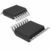
16-Lead Small Outline Integrated Circuit
(SOIC) JEDEC MS-012,0.150 Narrow
Green
16-Lead Quarter Size Outline Package
(QSOP) JEDEC MO-137 0.150 Inch Wide
Tape and Reel
RoHS
16-Lead Thin Shrink Small Outline Package
(TSSOP) JEDEC MO-153, 4mm Wide
Tape and Reel
Tape and Reel
Tubes
Tubes
For Fairchild’s definition of Eco Status, please visit: http://www.fairchildsemi.com/company/green/rohs_green.html.
© 1997 Fairchild Semiconductor Corporation
FST3257 • Rev. 1.0.3
www.fairchildsemi.com
FST3257 — Quad 2:1 Multiplexer / Demultiplexer Bus Switch
May 2009
�Figure 1. Logic Diagram
Figure 2. Connection Diagram
Pin Descriptions
Pin #
Names
Description
1
S
Select Input
2, 3, 5, 6, 10, 11, 13, 14
1B1, 1B2 ,2B1, 2B2, 3B1, 3B2, 4B1, 4B2
Bus B
4, 7, 9, 12
1A, 2A, 3A, 4A
Bus A
8
GND
Ground
15
/OE
Bus Switch Enables
16
VCC
Supply Voltage
Select Inputs
Bus Switch Enabled
Function
S
Logic Level HIGH
Disconnected
Logic Level LOW
Logic Level LOW
A=B1
Logic Level HIGH
Logic Level LOW
A=B2
FST3257 — Quad 2:1 Multiplexer / Demultiplexer Bus Switch
Pin Assignments
Truth Table
© 1997 Fairchild Semiconductor Corporation
FST3257 • Rev. 1.0.3
www.fairchildsemi.com
2
�Stresses exceeding the absolute maximum ratings may damage the device. The device may not function or be
operable above the recommended operating conditions and stressing the parts to these levels is not recommended.
In addition, extended exposure to stresses above the recommended operating conditions may affect device
reliability. The absolute maximum ratings are stress ratings only.
Symbol
Parameter
VCC
Supply Voltage
Min.
Max.
Unit
-0.5
+7.0
V
VS
DC Switch Voltage
-0.5
+7.0
V
VIN
DC Input Voltage
(1)
-0.5
+7.0
V
IIK
DC Input Current
-50
mA
DC Output Sink Current
128
mA
DC VCC/GND Current
±100
mA
+150
°C
IOUT
ICC/IGND
TSTG
Storage Temperature Range
-65
Note:
1. The input and output negative voltage ratings may be exceeded if the input and output diode current ratings are
observed.
Recommended Operating Conditions
The Recommended Operating Conditions table defines the conditions for actual device operation. Recommended
operating conditions are specified to ensure optimal performance to the datasheet specifications. Fairchild does not
recommend exceeding them or designing to Absolute Maximum Ratings.
Symbol
Parameter
Min.
Max.
Unit
3.0
5.5
V
VCC
Power Supply Operating
VIN
Input Voltage
0
5.5
V
Output Voltage
0
5.5
V
Switch Control Input
0
5
Switch I/O
0
DC
-40
+85
VOUT
tr,tf
Input Rise and Fall Time
TA
Free Air Operating Temperature
FST3257 — Quad 2:1 Multiplexer / Demultiplexer Bus Switch
Absolute Maximum Ratings
ns/V
°C
Note:
2. Unused control inputs must be held HIGH or LOW. They may not float.
© 1997 Fairchild Semiconductor Corporation
FST3257 • Rev. 1.0.3
www.fairchildsemi.com
3
�Symbol
VIK
Parameter
Conditions
Clamp Diode Voltage
IIN=-18mA
VIH
High-Level Input Voltage
VIL
Low-Level Input Voltage
IIN
Input Leakage Current
IOZ
Off-state Leakage Current
ICC
ΔICC
Switch On Resistance
(4)
TA=-40 to +85°C
Min.
(3)
Typ.
4.5
3.0 to 3.6
3.0 to 3.6
Units
Max.
-1.2
(5)
4.0 to 5.5
1.8
V
V
2.0
(5)
0.7
V
4.0 to 5.5
0.8
0 ≤ VIN ≤ 5.5
5.5
±1.0
µA
0 ≤ A, B ≤ VCC
5.5
±1.0
µA
3.3
(5)
VIN=0V, IIN=30mA
3.3
(5)
28
40
VIN=2.4V, IIN=15mA
3.3
(5)
200
230
VIN=2.4V, IIN=15mA
3.0
(5)
210
250
VIN=0V, IIN=64mA
RON
VCC (V)
13
20
Ω
VIN=0V, IIN=64mA
4.5
4
7
VIN=0V, IIN=30mA
4.5
4
7
VIN=2.4V, IIN=15mA
4.5
8
15
VIN=2.4V, IIN=15mA
4.0
11
20
Quiescent Supply Current
VIN=VCC or GND,
IOUT=0,
5.5
3
µA
Increase in ICC per input
One Input at 3.4V, Other
inputs at VCC or GND
5.5
2.5
mA
FST3257 — Quad 2:1 Multiplexer / Demultiplexer Bus Switch
DC Electrical Characteristics
Notes:
3. Typical values are at nominal VCC for the VCC range and TA=25°C.
4. Measured by the voltage drop between A and B pins at the indicated current through the switch. On resistance
is determined by the lower of the voltages on the A or B pins.
5. This parameter is guaranteed by design, but is not tested.
© 1997 Fairchild Semiconductor Corporation
FST3257 • Rev. 1.0.3
www.fairchildsemi.com
4
�TA=-40 to +85°C, CL= 50pF,
RU=RD=500Ω
Symbol
Parameter
Conditions
VCC= 4.5
to 5.5V
Min.
tPHL,tPLH
tPZH,tPZL
tPHZ,tPLZ
Propagation Delay
(6)
Bus to Bus
Propagation Delay
(6)
Select to Bus A
Output Enable
Time, Select to
Bus B
Output Enable
Time, Select to
Bus /OE
Output Disable
Time, Select to
Bus B
Output Disable
Time, Select to
Bus /OE
Max.
VCC=4.0V
Min.
Max.
Units
Figure
ns
Figure 3
Figure 4
ns
Figure 3
Figure 4
ns
Figure 3
Figure 4
VCC=3.0
(7)
to 3.6V
Min.
Max.
0.25
VIN=Open
0.25
VIN=7V for tPZL
VIN=Open for
tPZH
VIN=7V for tPLZ
VIN=Open for
tPHZ
1.0
5.0
1.5
5.3
0.25
1.0
6.8
1.0
7.9
5.5
1.0
8.5
1.0
9.9
5.6
1.5
9.9
Notes:
6. This parameter is guaranteed by design but is not tested. The bus switch contributes no propagation delay other
than the RC delay of the typical on resistance of the switch and the 50pF load capacitance, when driven by an
ideal voltage source (zero output impedance).
7. These parameters are guaranteed by design, but not tested.
FST3257 — Quad 2:1 Multiplexer / Demultiplexer Bus Switch
AC Electrical Characteristics
Capacitance
TA=+25°C, f=1MHz. Capacitance is characterized by not tested.
Symbol
CIN
Parameter
Conditions
Control Pin Input Capacitance
VCC=5.0V
A Port
CI/O
Input/Output Capacitance
B Port
A Port
B Port
© 1997 Fairchild Semiconductor Corporation
FST3257 • Rev. 1.0.3
VCC /OE=5.0V
VCC /OE=3.3V
Typ.
3.0
7.0
5.0
3.0
3.5
Max.
Units
pF
pF
pF
www.fairchildsemi.com
5
�Notes:
8. Input driven by 50Ω source terminated in 50Ω.
9. CL included load and stray capacitance.
10. Input PRR=1.0MHz, tw=500ns.
Figure 3. AC Test Circuit
FST3257 — Quad 2:1 Multiplexer / Demultiplexer Bus Switch
AC Loadings and Waveforms
Figure 4. AC Waveforms
© 1997 Fairchild Semiconductor Corporation
FST3257 • Rev. 1.0.3
www.fairchildsemi.com
6
�10.00
9.80
A
8.89
16
9
B
4.00
3.80
6.00
PIN ONE
NDICATOR
1.75
1
5.6
8
0.51
0.35
1.27
(0.30)
0.25
M
1.27
C B A
0.65
LAND PATTERN RECOMMENDATION
1.75 MAX
1.50
1.25
SEE DETAIL A
0.25
0.10
C
0.25
0.19
FST3257 — Quad 2:1 Multiplexer / Demultiplexer Bus Switch
Physical Dimensions
0.10 C
0.50
0.25 X 45°
NOTES: UNLESS OTHERWISE SPECIFIED
(R0.10)
GAGE PLANE
A) THIS PACKAGE CONFORMS TO JEDEC
MS-012, VARIATION AC, ISSUE C.
B) ALL DIMENSIONS ARE IN MILLIMETERS.
C) DIMENSIONS ARE EXCLUSIVE OF BURRS, MOLD
FLASH AND TIE BAR PROTRUSIONS
D) CONFORMS TO ASME Y14.5M-1994
E) LANDPATTERN STANDARD: SOIC127P600X175-16AM
F) DRAWING FILE NAME: M16AREV12.
(R0.10)
8°
0°
0.36
SEATING PLANE
0.90
0.50
(1.04)
DETAIL A
SCALE: 2:1
Figure 5. 16-Lead Small Outline Integrated Circuit (SOIC) JEDEC MS-012,0.150 Narrow
Package drawings are provided as a service to customers considering Fairchild components. Drawings may change in any manner
without notice. Please note the revision and/or date on the drawing and contact a Fairchild Semiconductor representative to verify
or obtain the most recent revision. Package specifications do not expand the terms of Fairchild’s worldwide terms and conditions, specifically
the warranty therein, which covers Fairchild products.
Always visit Fairchild Semiconductor’s online packaging area for the most recent package drawings:
http://www.fairchildsemi.com/packaging/.
© 1997 Fairchild Semiconductor Corporation
FST3257 • Rev. 1.0.3
www.fairchildsemi.com
7
�LAND PATTERN
RECOMMENDATION
TOP VIEW
FST3257 — Quad 2:1 Multiplexer / Demultiplexer Bus Switch
Physical Dimensions
END VIEW
SIDE VIEW
DETAIL A
Figure 6. 16-Lead Quarter Size Outline Package (QSOP) JEDEC MO-137 0.150 Inch Wide
Package drawings are provided as a service to customers considering Fairchild components. Drawings may change in any manner
without notice. Please note the revision and/or date on the drawing and contact a Fairchild Semiconductor representative to verify
or obtain the most recent revision. Package specifications do not expand the terms of Fairchild’s worldwide terms and conditions, specifically
the warranty therein, which covers Fairchild products.
Always visit Fairchild Semiconductor’s online packaging area for the most recent package drawings:
http://www.fairchildsemi.com/packaging/.
© 1997 Fairchild Semiconductor Corporation
FST3257 • Rev. 1.0.3
www.fairchildsemi.com
8
�5.00±0.10
4.55
5.90
4.45 7.35
0.65
4.4±0.1
1.45
5.00
0.11
FST3257 — Quad 2:1 Multiplexer / Demultiplexer Bus Switch
Physical Dimensions
12°
MTC16rev4
Figure 7. 16-Lead Thin Shrink Small Outline Package (TSSOP) MO-153, 4.4mm Wide
Package drawings are provided as a service to customers considering Fairchild components. Drawings may change in any manner
without notice. Please note the revision and/or date on the drawing and contact a Fairchild Semiconductor representative to verify
or obtain the most recent revision. Package specifications do not expand the terms of Fairchild’s worldwide terms and conditions, specifically
the warranty therein, which covers Fairchild products.
Always visit Fairchild Semiconductor’s online packaging area for the most recent package drawings:
http://www.fairchildsemi.com/packaging/.
© 1997 Fairchild Semiconductor Corporation
FST3257 • Rev. 1.0.3
www.fairchildsemi.com
9
�FST3257 — Quad 2:1 Multiplexer / Demultiplexer Bus Switch
© 1997 Fairchild Semiconductor Corporation
FST3257 • Rev. 1.0.3
www.fairchildsemi.com
10
�ON Semiconductor and
are trademarks of Semiconductor Components Industries, LLC dba ON Semiconductor or its subsidiaries in the United States and/or other countries.
ON Semiconductor owns the rights to a number of patents, trademarks, copyrights, trade secrets, and other intellectual property. A listing of ON Semiconductor’s product/patent
coverage may be accessed at www.onsemi.com/site/pdf/Patent−Marking.pdf. ON Semiconductor reserves the right to make changes without further notice to any products herein.
ON Semiconductor makes no warranty, representation or guarantee regarding the suitability of its products for any particular purpose, nor does ON Semiconductor assume any liability
arising out of the application or use of any product or circuit, and specifically disclaims any and all liability, including without limitation special, consequential or incidental damages.
Buyer is responsible for its products and applications using ON Semiconductor products, including compliance with all laws, regulations and safety requirements or standards,
regardless of any support or applications information provided by ON Semiconductor. “Typical” parameters which may be provided in ON Semiconductor data sheets and/or
specifications can and do vary in different applications and actual performance may vary over time. All operating parameters, including “Typicals” must be validated for each customer
application by customer’s technical experts. ON Semiconductor does not convey any license under its patent rights nor the rights of others. ON Semiconductor products are not
designed, intended, or authorized for use as a critical component in life support systems or any FDA Class 3 medical devices or medical devices with a same or similar classification
in a foreign jurisdiction or any devices intended for implantation in the human body. Should Buyer purchase or use ON Semiconductor products for any such unintended or unauthorized
application, Buyer shall indemnify and hold ON Semiconductor and its officers, employees, subsidiaries, affiliates, and distributors harmless against all claims, costs, damages, and
expenses, and reasonable attorney fees arising out of, directly or indirectly, any claim of personal injury or death associated with such unintended or unauthorized use, even if such
claim alleges that ON Semiconductor was negligent regarding the design or manufacture of the part. ON Semiconductor is an Equal Opportunity/Affirmative Action Employer. This
literature is subject to all applicable copyright laws and is not for resale in any manner.
PUBLICATION ORDERING INFORMATION
LITERATURE FULFILLMENT:
Literature Distribution Center for ON Semiconductor
19521 E. 32nd Pkwy, Aurora, Colorado 80011 USA
Phone: 303−675−2175 or 800−344−3860 Toll Free USA/Canada
Fax: 303−675−2176 or 800−344−3867 Toll Free USA/Canada
Email: orderlit@onsemi.com
© Semiconductor Components Industries, LLC
N. American Technical Support: 800−282−9855 Toll Free
USA/Canada
Europe, Middle East and Africa Technical Support:
Phone: 421 33 790 2910
Japan Customer Focus Center
Phone: 81−3−5817−1050
www.onsemi.com
1
ON Semiconductor Website: www.onsemi.com
Order Literature: http://www.onsemi.com/orderlit
For additional information, please contact your local
Sales Representative
www.onsemi.com
�


 工商网监
湘ICP备2023018690号
工商网监
湘ICP备2023018690号
