DATA SHEET
www.onsemi.com
Low-Voltage, Dual-Supply,
8-Bit, Signal Translator with
Configurable Voltage Supplies,
Bushold Data Inputs,
3-State Outputs and 26 W
Series Resistors in the
B-Port Outputs
WQFN24, 4.5 x 3.5, 0.5P
CASE 510CE
MARKING DIAGRAM
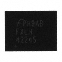
FXLH42245
$Y&Z&2&K
FXLH
42245
Description
The FXLH42245 is a configurable dual−voltage−supply translator
designed for bi−directional voltage translation of signals between two
voltage levels. The device allows translation between voltages as high
as 3.6 V to as low as 1.1 V. The A port tracks the VCCA level and the B
port tracks the VCCB level. Both ports are designed to accept supply
voltage levels from 1.1 V to 3.6 V. This allows for bi−directional
voltage translation over a variety of voltage levels: 1.2 V, 1.5 V, 1.8 V,
2.5 V, and 3.3 V.
The device remains in 3−state until both VCCs reach active levels,
allowing either VCC to be powered−up first. The device also contains
power−down control circuits that place the device in 3−state if either
VCC is removed.
The Transmit/Receive (T/R) input determines the direction of data
flow through the device. The OE input, when HIGH, disables both
the A and B ports by placing them in a 3−state condition.
The FXLH42245 is designed with the control pins (T/R and OE)
supplied by VCCA.
$Y
&Z
&2
&K
FXLH42245
= onsemi logo
= Assembly Plant Code
= 2−Digit Date Code
= 2−Digits Lot Run Traceability Code
= Specific Device Code
ORDERING INFORMATION
Device
Package
Shipping†
FXLH42245MPX
WQFN24
(Pb−Free)
3000 / Tape &
Reel
†For information on tape and reel specifications,
including part orientation and tape sizes, please
refer to our Tape and Reel Packaging Specification
Brochure, BRD8011/D.
Features
•
•
•
•
•
•
•
•
•
•
•
Bi−Directional Interface between Two Levels from 1.1 V to 3.6 V
Fully Configurable, Inputs Track VCC Level
Non−Preferential Power−Up; Either VCC May Be Powered−Up First
Outputs Remain in 3−State Until Active VCC Level is Reached
Outputs Switch to 3−State if Either VCC is at GND
Bushold on Data Inputs Eliminates the need for External
Pull−Up / Pull−Down Resistors
26 W Output Series Resistors on the B Port to Reduce Line Noise
Power−Off Protection
Control Input (T/R, OE) Levels are Referenced to VCCA Voltage
Packaged in 24−Pin MLP
ESD Protection Exceeds:
♦ 4 kV Human Body Model
(JESD22−A114 & Mil Std 883e 3015.7)
♦ 8 kV Human Body Model I/O to GND
(JESD22−A114 & Mil Std 883e 3015.7)
♦ 1 kV Charge Device Model (ESD STM 5.3)
♦ 200 V Machine Model
(JESD22−A115 & ESD STM5.2)
© Semiconductor Components Industries, LLC, 2004
June, 2022 − Rev. 2
1
Publication Order Number:
FXLH42245/D
�FXLH42245
PIN CONFIGURATION
Figure 1. Pin Configuration (Top Through View)
PIN DEFINITIONS
ÁÁÁÁÁÁÁÁÁÁÁÁÁÁÁÁÁÁÁÁÁÁÁÁÁÁÁÁÁÁÁÁÁÁÁ
ÁÁÁÁÁÁÁÁÁÁÁÁÁÁÁÁÁÁÁÁÁÁÁÁÁÁÁÁÁÁÁÁÁÁÁ
ÁÁÁÁÁÁÁÁÁÁÁÁÁÁÁÁÁÁÁÁÁÁÁÁÁÁÁÁÁÁÁÁÁÁÁ
ÁÁÁÁÁÁÁÁÁÁÁÁÁÁÁÁÁÁÁÁÁÁÁÁÁÁÁÁÁÁÁÁÁÁÁ
ÁÁÁÁÁÁÁÁÁÁÁÁÁÁÁÁÁÁÁÁÁÁÁÁÁÁÁÁÁÁÁÁÁÁÁ
ÁÁÁÁÁÁÁÁÁÁÁÁÁÁÁÁÁÁÁÁÁÁÁÁÁÁÁÁÁÁÁÁÁÁÁ
ÁÁÁÁÁÁÁÁÁÁÁÁ
ÁÁÁÁÁÁÁÁÁÁÁÁÁÁÁÁÁÁÁÁÁÁÁÁ
ÁÁÁÁÁÁÁÁÁÁÁÁÁÁÁÁÁÁÁÁÁÁÁ
ÁÁÁÁÁÁÁÁÁÁÁ
Pin No.
Name
1
VCCA
2
T/R
3, 4, 5, 6, 7, 8, 9, 10
A0, A1, A2, A3, A4, A5, A6, A7
11, 12, 13
GND
14, 15, 16, 17, 18, 19, 20, 21
B7, B6, B5, B4, B3, B2, B1, B0
22
OE
23, 24
VCCB
Description
Side−A Power Supply
Transmit / Receive Input
Side−A Inputs or 3−State Outputs
Ground
Side−B Inputs or 3−State Outputs
Output Enable Input
Side−B Power Supply
TRUTH TABLE
Inputs
OE
T/R
Description
LOW Voltage Level
LOW Voltage Level
Bus B Data to Bus A
LOW Voltage Level
HIGH Voltage Level
Bus A Date to Bus B
HIGH Voltage Level
Don’t Care
3−State
www.onsemi.com
2
�FXLH42245
ABSOLUTE MAXIMUM RATINGS
Symbol
VCCA
Parameter
Condition
Min
Max
Unit
−0.5
4.6
V
−0.5
4.6
I/O Port A
−0.5
VCCA + 0.5
I/O Port B
−0.5
VCCB + 0.5
Control Inputs (T/R, OE)
−0.5
4.6
Output 3−State
−0.5
4.6
Output Active (An)
−0.5
VCCA + 0.5
Output Active (Bn)
−0.5
VCCB + 0.5
Supply Voltage
VCCB
VI
VO
DC Input Voltage
Output Voltage (Note 1)
V
V
IIK
DC Input Diode Current
VI < 0 V
−50
mA
IOK
DC Output Diode Current
VO < 0 V
−50
mA
VO > VCC
50
IOH/IOL
ICC
DC Output Source/Sink Current
±50
mA
DC VCC or Ground Current per Supply Pin
±100
mA
+150
°C
4
kV
TSTG
Storage Temperature Range
ESD
Electrostatic Discharge
Capability
−65
Human Body Model,
JESD22−A114,
Mil Std 883e 3015.7
I/O to GND
8
Charged Device Model, JESD22−C101, STM 5.3
1
Machine Model, JESD22−A115, STM 5.2
200
V
Stresses exceeding those listed in the Maximum Ratings table may damage the device. If any of these limits are exceeded, device functionality
should not be assumed, damage may occur and reliability may be affected.
1. I/O absolute maximum ratings must be observed.
RECOMMENDED OPERATING CONDITIONS
Symbol
Parameter
Conditions
Min
Max
Unit
1.1
3.6
V
V
VCC
Power Supply
Operating VCCA or VCCB
VI
Input Voltage
Port A
0
VCCA
Port B
0
VCCB
Control Input (T/R, OE)
0
VCCA
IOH/IOL
Output Current
Port A
VCCA
Port B
VCCB
Resistor Outputs
3.0 V to 3.6 V
±24
2.3 V to 2.7 V
±18
1.65 V to 1.95 V
±6
1.40 V to 1.65 V
±2
1.1 V to 1.4. V
±0.5
3.0 V to 3.6 V
±14
2.3 V to 2.7 V
±8
1.65 V to 1.95 V
±3
1.40 V to 1.65 V
±1
1.1 V to 1.4. V
TA
DV/Dt
Operating Temperature, Free Air
Input Edge Rate
±0.25
−40
VCCA/B = 1.1 V to 3.6 V
mA
+85
°C
10
ns/V
Functional operation above the stresses listed in the Recommended Operating Ranges is not implied. Extended exposure to stresses beyond
the Recommended Operating Ranges limits may affect device reliability.
2. All unused inputs must be held at VCCI or GND.
www.onsemi.com
3
�FXLH42245
ELECTRICAL CHARACTERISTICS
Symbol
VIH
Parameter
HIGH Level Input
(Note 3)
Conditions
Data Inputs An, Bn
Control Pins OE, T/R
(Referenced to VCCA)
VIL
LOW Level Input
(Note 3)
Data Inputs An, Bn
HIGH Level Output
B Port
(Note 4)
HIGH Level Output
A Port
(Note 4)
VCCO (V)
Min
Max
Unit
1.1 to 3.6
2.0
−
V
2.30 to 2.70
1.6
−
1.65 to 2.30
0.65 x VCCI
−
1.40 to 1.65
0.65 x VCCI
−
1.10 to 1.40
0.9 x VCCI
−
2.70 to 3.60
1.1 to 3.6
2.0
−
2.30 to 2.70
1.6
−
1.65 to 2.30
0.65 x VCCA
−
1.40 to 1.65
0.65 x VCCA
−
1.10 to 1.40
0.9 x VCCA
−
−
0.8
2.70 to 3.60
1.1 to 3.6
2.30 to 2.70
Control Pins OE, T/R
(Referenced to VCCA)
VOH
VCCI (V)
2.70 to 3.60
−
0.7
1.65 to 2.30
−
0.35 x VCCI
1.40 to 1.65
−
0.35 x VCCI
1.10 to 1.40
−
0.10 x VCCI
−
0.8
2.30 to 2.70
−
0.7
1.65 to 2.30
−
0.35 x VCCA
1.40 to 1.65
−
0.35 x VCCA
1.10 to 1.40
−
0.10 x VCCA
2.70 to 3.60
1.1 to 3.6
1.1 to 3.6
1.1 to 3.6
VCC0 to 0.2
−
IOH = −6 mA
2.7
2.7
2.2
−
IOH = −8 mA
3.0
3.0
2.4
−
IOH = −12 mA
3.0
3.0
2.2
−
IOH = −4 mA
2.3
2.3
2.0
−
IOH = −6 mA
2.3
2.3
1.8
−
IOH = −8 mA
2.3
2.3
1.7
−
IOH = −3 mA
1.65
1.65
1.25
−
IOH = −1 mA
1.4
1.4
1.05
−
IOH = −0.25 mA
1.1
1.1
0.75 x VCC0
−
IOH = −100 mA
1.1 to 3.6
1.1 to 3.6
VCC0 to 0.2
−
IOH = −12 mA
2.7
2.7
2.2
−
IOH = −18 mA
3.0
3.0
2.4
−
IOH = −24 mA
3.0
3.0
2.2
−
IOH = −6 mA
2.3
2.3
2.0
−
IOH = −12 mA
2.3
2.3
1.8
−
IOH = −100 mA
IOH = −18 mA
2.3
2.3
1.7
−
IOH = −6 mA
1.65
1.65
1.25
−
IOH = −2 mA
1.4
1.4
1.05
−
IOH = −0.5 mA
1.1
1.1
0.75 x VCC0
−
www.onsemi.com
4
V
V
�FXLH42245
ELECTRICAL CHARACTERISTICS (continued)
Symbol
VOL
Parameter
LOW Level Output
B Port
(Note 4)
LOW Level Output
A Port
(Note 4)
VCCI (V)
VCCO (V)
Min
Max
Unit
1.1 to 3.6
1.1 to 3.6
−
0.2
V
IOH = 6 mA
2.7
2.7
−
0.4
IOH = 8 mA
3.0
3.0
−
0.55
IOH = 12 mA
3.0
3.0
−
0.80
IOH = 6 mA
2.3
2.3
−
0.4
Conditions
IOH = 100 mA
IOH = 8 mA
2.3
2.3
−
0.6
IOH = 3 mA
1.65
1.65
−
0.3
IOH = 1 mA
1.4
1.4
−
0.35
IOH = 0.25 mA
1.1
1.1
−
0.3 x VCC0
IOH = 100 mA
1.1 to 3.6
1.1 to 3.6
−
0.2
IOH = 12 mA
2.7
2.7
−
0.4
IOH = 18 mA
3.0
3.0
−
0.4
IOH = 24 mA
3.0
3.0
−
0.55
IOH = 12 mA
2.3
2.3
−
0.4
IOH = 18 mA
2.3
2.3
−
0.6
IOH = 6 mA
1.65
1.65
−
0.3
IOH = 2 mA
1.4
1.4
−
0.35
IOH = 0.5 mA
IL
II(HOLD)
II(OD)
1.1
1.1
−
0.3 x VCC0
1.1 to 3.6
3.6
−
±1.0
mA
VIN = 0.8
3.0
3.0
75
−
mA
VIN = 2.0
3.0
3.0
−75
−
VIN = 0.7
2.3
2.3
45
−
VIN = 1.6
2.3
2.3
−45
−
VIN = 0.57
1.65
1.65
25
−
VIN = 10.7
1.65
1.65
−25
−
VIN = 0.49
1.4
1.4
11
−
VIN = 0.91
1.4
1.4
−11
−
VIN = 0.11
1.1
1.1
−
4
VIN = 0.99
1.1
1.1
−
−4
(Note 5)
3.6
3.6
450
−
(Note 6)
3.6
3.6
−450
−
(Note 5)
2.7
2.7
300
−
Input Leakage Current,
Control Pins
VI = VCCA or GND
Bushold Input
Minimum Drive
Current
Bushold Input
Over−Drive
Current−to−Current
State
(Note 6)
2.7
2.7
−300
−
(Note 5)
1.95
1.95
200
−
(Note 6)
1.95
1.95
−200
−
(Note 5)
1.6
1.6
120
−
(Note 6)
1.6
1.6
−120
−
(Note 5)
1.4
1.4
80
−
(Note 6)
1.4
1.4
−80
−
www.onsemi.com
5
mA
�FXLH42245
ELECTRICAL CHARACTERISTICS (continued)
Symbol
IOFF
IOZ
ICCA/B
ICCZ
Conditions
VCCI (V)
VCCO (V)
Min
Max
Unit
Power Off Leakage
Current
An, VI or VO = 0 V to 3.6 V
0
3.6
−
±10
mA
Bn, VI or VO = 0 V to 3.6 V
3.6
0
−
±10
3−State Output
Leakage
(VO, VCC or GND
VI = VIH or VIL)
An, Bn, OE = VIH
3.6
3.6
−
±10
Bn, OE = Don’t Care
(Note 7)
0
3.6
−
±10
An, OE = Don’t Care
(Note 7)
3.6
0
−
±10
1.1 to 3.6
1.1 to 3.6
−
20
mA
1.1 to 3.6
1.1 to 3.6
−
20
mA
0
1.1 to 3.6
−
−10
mA
1.1 to 3.6
0
−
10
1.1 to 3.6
0
−
−10
0
1.1 to 3.6
−
10
3.6
3.6
−
500
Parameter
Quiescent Supply
Current
(Note 8)
ICCA
VI = VCCA or GND; IO = 0
ICCB
DICCA/B
VI = VCCI or GND; IO = 0
VI = VCCB or GND; IO = 0
Increase in ICC per
Input; Other Inputs at
VCC or GND
VIH = 3.0
mA
mA
mA
Product parametric performance is indicated in the Electrical Characteristics for the listed test conditions, unless otherwise noted. Product
performance may not be indicated by the Electrical Characteristics if operated under different conditions.
3. VCCI = the VCC associated with the data input under test.
4. VCCO = the VCC associated with the output under test.
5. An external driver must source at least the specified current to switch LOW−to−HIGH.
6. An external driver must source at least the specified current to switch HIGH−to−LOW.
7. Don’t care = any valid logic level.
8. Reflects current per supply, VCCA or VCCB.
AC ELECTRICAL CHARACTERISTICS
VCCA = 3.0 V to 3.6 V
TA = −40°C to +85°C
VCCB = 3.0 V
to 3.6 V
VCCB = 2.3 V
to 2.7 V
Min
Max
Min
Max
Min
tPLH, tPHL Propagation
Delay A to B
0.5
3.9
0.5
4.5
Propagation
Delay B to A
0.2
3.5
0.2
Output Enable
OE−to−B
0.7
4.8
Output Enable
OE−to−A
0.5
Output Enable
OE−to−B
Output Enable
OE−to−A
Symbol
tPZL, tPZH
tPHZ, tPZL
Parameter
VCCB = 1.65 V
to 1.95 V
VCCB = 1.4 V
to 1.6 V
VCCB = 1.1 V
to 1.3 V
Max
Min
Max
Min
Max
Unit
0.9
5.9
1.0
7.4
1.6
22.0
ns
3.8
0.3
4.0
0.5
4.3
0.8
13.0
1.0
5.1
1.5
6.7
1.5
7.1
2.0
18.0
4.0
0.5
4.0
0.5
4.0
0.5
4.0
0.5
4.0
0.4
4.3
0.4
4.4
0.9
5.2
1.7
6.8
2.0
19.0
0.2
3.7
0.2
3.7
0.2
3.7
0.2
3.7
0.2
3.7
www.onsemi.com
6
ns
ns
�FXLH42245
AC ELECTRICAL CHARACTERISTICS (continued)
VCCA = 2.3 V to 2.7 V
TA = −40°C to +85°C
VCCB = 3.0 V
to 3.6 V
VCCB = 2.3 V
to 2.7 V
Min
Max
Min
Max
Min
tPLH, tPHL Propagation
Delay A to B
0.5
4.3
0.6
4.8
Propagation
Delay B to A
0.3
3.9
0.4
Output Enable
OE−to−B
0.8
5.1
Output Enable
OE−to−A
0.6
Output Enable
OE−to−B
Output Enable
OE−to−A
Symbol
tPZL, tPZH
tPHZ, tPZL
Parameter
VCCB = 1.65 V
to 1.95 V
VCCB = 1.4 V
to 1.6 V
VCCB = 1.1 V
to 1.3 V
Max
Min
Max
Min
Max
Unit
0.9
6.0
1.0
7.6
1.6
22.0
ns
4.2
0.5
4.5
0.5
4.8
1.0
7.0
1.0
5.5
1.5
6.9
1.5
7.4
2.0
19.0
4.5
0.6
4.5
0.6
4.5
0.6
4.5
0.6
4.5
0.4
4.6
0.4
4.8
0.9
5.3
1.7
7.1
2.0
19.0
0.2
4.0
0.2
4.0
0.2
4.0
0.2
4.0
0.2
4.0
ns
ns
VCCA = 1.65 V to 1.95 V
TA = −40°C to +85°C
VCCB = 3.0 V
to 3.6 V
VCCB = 2.3 V
to 2.7 V
Min
Max
Min
Max
Min
tPLH, tPHL Propagation
Delay A to B
0.5
4.6
0.7
5.1
Propagation
Delay B to A
0.5
5.4
0.5
Output Enable
OE−to−B
0.8
5.4
Output Enable
OE−to−A
1.0
Output Enable
OE−to−B
Output Enable
OE−to−A
Symbol
tPZL, tPZH
tPHZ, tPZL
Parameter
VCCB = 1.65 V
to 1.95 V
VCCB = 1.4 V
to 1.6 V
VCCB = 1.1 V
to 1.3 V
Max
Min
Max
Min
Max
Unit
1.1
6.2
1.1
7.8
1.7
22.0
ns
5.6
0.8
5.7
1.0
6.0
1.2
8.0
1.0
5.9
1.5
7.3
1.5
7.7
2.0
20.0
6.7
1.0
6.7
1.0
6.7
1.0
6.7
1.0
6.7
0.4
4.7
0.4
4.9
1.0
5.4
1.7
7.2
2.0
19.0
0.5
5.0
0.5
5.0
0.5
5.0
0.5
5.0
0.5
5.0
www.onsemi.com
7
ns
ns
�FXLH42245
AC ELECTRICAL CHARACTERISTICS (continued)
VCCA = 1.4 V to 1.6 V
TA = −40°C to +85°C
VCCB = 3.0 V
to 3.6 V
VCCB = 2.3 V
to 2.7 V
Min
Max
Min
Max
Min
tPLH, tPHL Propagation
Delay A to B
0.7
4.8
0.8
5.3
Propagation
Delay B to A
0.6
6.8
0.8
Output Enable
OE−to−B
1.1
5.8
Output Enable
OE−to−A
1.0
Output Enable
OE−to−B
Output Enable
OE−to−A
Symbol
tPZL, tPZH
tPHZ, tPZL
Parameter
VCCB = 1.65 V
to 1.95 V
VCCB = 1.4 V
to 1.6 V
VCCB = 1.1 V
to 1.3 V
Max
Min
Max
Min
Max
Unit
1.2
6.4
1.3
7.9
1.7
22.0
ns
6.9
0.9
7.1
1.0
7.3
1.2
9.5
1.3
6.3
1.5
7.8
2.0
8.1
2.0
20.0
7.5
1.0
7.5
1.0
7.5
1.0
7.5
1.0
7.5
0.6
4.8
0.6
5.1
1.1
5.8
2.0
7.7
2.0
18.0
1.0
6.0
1.0
6.0
1.0
6.0
1.0
6.0
0.5
6.0
ns
ns
VCCA = 1.1 V to 1.3 V
TA = −40°C to +85°C
VCCB = 3.0 V
to 3.6 V
VCCB = 2.3 V
to 2.7 V
Min
Max
Min
Max
Min
tPLH, tPHL Propagation
Delay A to B
1.0
13.8
1.0
7.8
Propagation
Delay B to A
1.4
22.0
1.4
Output Enable
OE−to−B
1.5
12.6
Output Enable
OE−to−A
2.0
Output Enable
OE−to−B
Output Enable
OE−to−A
Symbol
tPZL, tPZH
tPHZ, tPZL
Parameter
VCCB = 1.65 V
to 1.95 V
VCCB = 1.4 V
to 1.6 V
VCCB = 1.1 V
to 1.3 V
Max
Min
Max
Min
Max
Unit
1.0
8.4
1.0
10.4
2.0
24.0
ns
22.0
1.5
22.0
1.5
22.0
2.0
24.0
1.5
9.6
1.5
10.6
2.0
11.6
2.0
24.0
22.0
2.0
22.0
2.0
22.0
2.0
22.0
2.0
22.0
1.2
15.0
0.9
7.6
1.2
8.6
2.0
10.6
3.0
21.0
2.0
15.0
2.0
12.0
2.0
12.0
2.0
12.0
2.0
12.0
ns
ns
Product parametric performance is indicated in the Electrical Characteristics for the listed test conditions, unless otherwise noted. Product
performance may not be indicated by the Electrical Characteristics if operated under different conditions.
CAPACITANCE
Symbol
Parameter
Conditions
Typical (TA = 255C)
Unit
CIN
Input Capacitance Control Pins
(OE, T/R)
VCCA = VCCB = 3.3 V,
VI = 0 V or VCCA/B
4
pF
CI/O
Input / Output Capacitance
An, Bn Port
VCCA = VCCB = 3.3 V,
VI = 0 V or VCCA/B
5
pF
CPD
Power Dissipation Capacitance
VCCA = VCCB = 3.3 V,
VI = 0 V or VCC, f = 10 MHz
20
pF
www.onsemi.com
8
�FXLH42245
AC LOADINGS AND WAVEFORMS
VCC
TEST
SIGNAL
Rtr1
OPEN
DUT
GND
VCC2
tPLH, tPHL
tPZH, tPHZ
tPZL, tPLZ
RL
CL
Figure 2. AC Test Circuit
Table 1. TEST CIRCUIT PARAMETERS
Test
Switch
tPLH, tPHL
Open
tPLZ, tPZL
VCC0 • 2 at VCC0 = 3.3 + 0.3 V, 2.5 V + 0.2 V,
1.8 V + 0.15 V, 1.5 V + 0.1 V, 1.2 V + 0.1 V
tPHZ, tPZH
GND
Table 2. AC LOAD TABLE
VCC0
CL
RL
Rtr1
1.2 V ± 0.1 V
15 pF
2 kW
2 kW
1.5 V ± 0.1 V
15 pF
2 kW
2 kW
1.8 V ± 0.15 V
30 pF
500 W
500 W
2.5 V ± 0.2 V
30 pF
500 W
500 W
3.3 V ± 0.3 V
30 pF
500 W
500 W
9. Input tR = tF = 2.0 ns, 10% to 90%
10. Input tR = tF = 2.0 ns, 10% to 90%
Figure 3. Waveform for Inverting and Non−
Inverting Functions
Figure 4. 3−State Output High Enable and
Disable for Low Voltage Logic
11. Input tR = tF = 2.0 ns, 10% to 90%
Figure 5. 3−State Output High Enable and
Disable for Low Voltage Logic
www.onsemi.com
9
�FXLH42245
Table 3.
VCC
Symbol
3.3 V + 0.3 V
2.5 V + 0.2 V
1.8 V + 0.15 V
1.5 V + 0.1 V
1.2 V + 0.1 V
VMI
VCCI/2
VCCI/2
VCCI/2
VCCI/2
VCCI/2
VMO
VCC0/2
VCC0/2
VCC0/2
VCC0/2
VCC0/2
VX
VOH − 0.3 V
VOH − 0.15 V
VOH − 0.15 V
VOH − 0.1 V
VOH − 0.1 V
VY
VOL + 0.3 V
VOL + 0.15 V
VOL + 0.15 V
VOL + 0.1 V
VOL + 0.1 V
12. For VMI VCCO = VCCA for control pins T/R and OE or VCCA/2.
FUNCTIONAL DESCRIPTION
Power−Up/Power−Down Sequencing
The recommended power−down sequence is:
1. Drive OE input HIGH to disable the device.
2. Remove power from either VCC.
3. Remove power from the other VCC.
FXL translators offer an advantage in that either VCC may
be powered up first. This benefit derives from the chip
design. When either VCC is at 0 V, outputs are in a
High−impedance state. The control inputs (T/R and OE) are
designed to track the VCCA supply. A pull−up resistor tying
OE to VCCA should be used to ensure that bus contention,
excessive currents, or oscillations do not occur during
power−up/power−down. The size of the pull−up resistor is
based upon the current−sinking capability of the OE driver.
The recommended power−up sequence is:
1. Apply power to either VCC.
2. Apply power to the T/R input (logic HIGH for A−to−B
operation; logic LOW for B−to−A operation) and to
the respective data inputs (A port or B port). This may
occur at the same time as step 1.
3. Apply power to the other VCC.
4. Drive the OE input LOW to enable the device.
www.onsemi.com
10
�MECHANICAL CASE OUTLINE
PACKAGE DIMENSIONS
WQFN24 4.5x3.5, 0.5P
CASE 510CE
ISSUE O
DOCUMENT NUMBER:
DESCRIPTION:
98AON13646G
WQFN24 4.5X3.5, 0.5P
DATE 31 AUG 2016
Electronic versions are uncontrolled except when accessed directly from the Document Repository.
Printed versions are uncontrolled except when stamped “CONTROLLED COPY” in red.
PAGE 1 OF 1
ON Semiconductor and
are trademarks of Semiconductor Components Industries, LLC dba ON Semiconductor or its subsidiaries in the United States and/or other countries.
ON Semiconductor reserves the right to make changes without further notice to any products herein. ON Semiconductor makes no warranty, representation or guarantee regarding
the suitability of its products for any particular purpose, nor does ON Semiconductor assume any liability arising out of the application or use of any product or circuit, and specifically
disclaims any and all liability, including without limitation special, consequential or incidental damages. ON Semiconductor does not convey any license under its patent rights nor the
rights of others.
© Semiconductor Components Industries, LLC, 2019
www.onsemi.com
�onsemi,
, and other names, marks, and brands are registered and/or common law trademarks of Semiconductor Components Industries, LLC dba “onsemi” or its affiliates
and/or subsidiaries in the United States and/or other countries. onsemi owns the rights to a number of patents, trademarks, copyrights, trade secrets, and other intellectual property.
A listing of onsemi’s product/patent coverage may be accessed at www.onsemi.com/site/pdf/Patent−Marking.pdf. onsemi reserves the right to make changes at any time to any
products or information herein, without notice. The information herein is provided “as−is” and onsemi makes no warranty, representation or guarantee regarding the accuracy of the
information, product features, availability, functionality, or suitability of its products for any particular purpose, nor does onsemi assume any liability arising out of the application or use
of any product or circuit, and specifically disclaims any and all liability, including without limitation special, consequential or incidental damages. Buyer is responsible for its products
and applications using onsemi products, including compliance with all laws, regulations and safety requirements or standards, regardless of any support or applications information
provided by onsemi. “Typical” parameters which may be provided in onsemi data sheets and/or specifications can and do vary in different applications and actual performance may
vary over time. All operating parameters, including “Typicals” must be validated for each customer application by customer’s technical experts. onsemi does not convey any license
under any of its intellectual property rights nor the rights of others. onsemi products are not designed, intended, or authorized for use as a critical component in life support systems
or any FDA Class 3 medical devices or medical devices with a same or similar classification in a foreign jurisdiction or any devices intended for implantation in the human body. Should
Buyer purchase or use onsemi products for any such unintended or unauthorized application, Buyer shall indemnify and hold onsemi and its officers, employees, subsidiaries, affiliates,
and distributors harmless against all claims, costs, damages, and expenses, and reasonable attorney fees arising out of, directly or indirectly, any claim of personal injury or death
associated with such unintended or unauthorized use, even if such claim alleges that onsemi was negligent regarding the design or manufacture of the part. onsemi is an Equal
Opportunity/Affirmative Action Employer. This literature is subject to all applicable copyright laws and is not for resale in any manner.
PUBLICATION ORDERING INFORMATION
LITERATURE FULFILLMENT:
Email Requests to: orderlit@onsemi.com
onsemi Website: www.onsemi.com
◊
TECHNICAL SUPPORT
North American Technical Support:
Voice Mail: 1 800−282−9855 Toll Free USA/Canada
Phone: 011 421 33 790 2910
Europe, Middle East and Africa Technical Support:
Phone: 00421 33 790 2910
For additional information, please contact your local Sales Representative
�


 工商网监
湘ICP备2023018690号
工商网监
湘ICP备2023018690号
