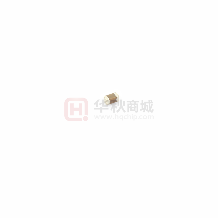
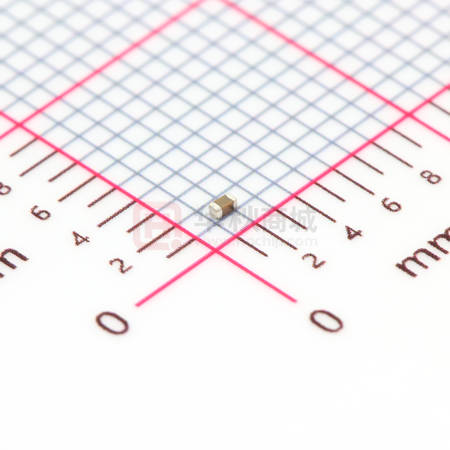
Chip Monolithic Ceramic Capacitor for General
GRM155R61A105KE01_ (0402, X5R:EIA, 1uF, DC10V)
_: packaging code
Reference Sheet
1.Scope
This product specification is applied to Chip Monolithic Ceramic Capacitor used for General Electronic equipment.
2.MURATA Part NO. System
(Ex.)
GRM
15
5
(2)T
Dimensions
(1)L/W
Dimensions
R6
1A
(4)Rated
Voltage
(3)Temperature
Characteristics
105
K
(5)Nominal
Capacitance
(6)Capacitance
Tolerance
E01
(7)Murata’s
Control Code
3. Type & Dimensions
(Unit:mm)
g
(1)-1 L
(1)-2 W
(2) T
e
1.0±0.05
0.5±0.05
0.5±0.05
0.15 to 0.35
0.3 min.
4.Rated value
(3) Temperature Characteristics
(Public STD Code):X5R(EIA)
Temp. coeff
Temp. Range
or Cap. Change
(Ref.Temp.)
-15 to 15 %
-55 to 85 °C
(25 °C)
(4)
Rated
Voltage
DC 10 V
(6)
(5) Nominal
Capacitance
Capacitance
Tolerance
1 uF
±10 %
Specifications and Test
Methods
(Operating
Temp. Range)
-55 to 85 °C
5.Package
mark
D
W
J
(8) Packaging
f180mm Reel
PAPER W8P2
f180mm Reel
PAPER W8P1
f330mm Reel
PAPER W8P2
Packaging Unit
10000 pcs./Reel
20000 pcs./Reel
50000 pcs./Reel
Product specifications in this catalog are as of Mar.6,2016,and are subject to change or obsolescence without notice.
Please consult the approval sheet before ordering.
Please read rating and !Cautions first.
GRM155R61A105KE01-01
1
D
(8)Packaging
Code
�■ Specifications and Test Methods
Item
No
1
Rated Voltage
Test Method
(Ref. Standard:JIS C 5101, IEC60384)
Specification
Shown in Rated value.
The rated voltage is defined as the maximum voltage which may be
applied continuously to the capacitor.
When AC voltage is superimposed on DC voltage, VP-P or VO-P,
whichever is larger, should be maintained within the rated voltage
range.
2
Appearance
No defects or abnormalities.
Visual inspection.
3
Dimension
Within the specified dimensions.
Using calipers. (GRM02 size is based on Microscope)
4
Voltage proof
No defects or abnormalities.
Measurement Point
Test Voltage
:Between the terminations
: 250% of the rated voltage
Applied Time
: 1 to 5 s
Charge/discharge current : 50mA max.
5
Insulation Resistance(I.R.)
More than 50Ω ∙ F
Measurement Point
: Between the terminations
Measurement Voltage
: DC Rated Voltage
Charging Time
: 1 min
Charge/discharge current : 50mA max.
Measurement Temperature :Room Temperature
6
Capacitance
Shown in Rated value.
Measurement Temperature :Room Temperature
7
Dissipation Factor (D.F.)
B1,R1,B3,R6,R7,C6,C7,C8,E7,D7 : 0.1 max.
Capacitance
C≦10μF
(10V min.)
C≦10μF
(6.3V max.)
D8,GRM31CR60J107 : 0.15 max
GRM31CR71E106 : 0.125
max
Frequency
Voltage
1.0+/-0.1kHz
1.0+/-0.2Vrms
1.0+/-0.1kHz
0.5+/-0.1Vrms
120+/-24Hz
0.5+/-0.1Vrms
C>10μF
8
Temperature
No bias
B1,B3 : Within +/-10%
(-25°C to +85°C)
(-55°C to +125°C)
The capacitance change should be measured after 5 min.
Characteristics
R1,R7 : Within +/-15%
of Capacitance
R6
: Within +/-15%
(-55°C to +85°C)
at each specified temp. stage.
In case of applying voltage, the capacitance change should be
C6
: Within +/-22%
(-55°C to +85°C)
measured after 1 min. with applying voltage in equilibration of
C7
: Within+/-22%
(-55°C to +125°C)
each temp. stage.
C8
: Within +/-22%
(-55°C to +105°C)
Capacitance value as a reference is the value in step 3.
E7
: Within +22/-56%
(-55°C to +125°C)
D7
: Within +22/-33%
(-55°C to +125°C)
D8
: Within +22/-33%
(-55°C to +105°C)
· Measurement Voltage : 0.5+/-0.1Vrms
Step
1
Temperature(C)
Reference Temp.+/-2
Min.Operating Temp. +/-3
50% of
B1: Within +10/-30%
2
the rated
R1: Within +15/-40%
3
Reference Temp. +/-2
4
5
Max.Operating Temp. +/-3
Reference Temp. +/-2
6
Min.Operating Temp. +/-3
7
Reference Temp. +/-2
8
Max.Operating Temp.+/-3
voltage
Applying Voltage(VDC)
No bias
50% of
the rated voltage
(For B1,R1)
・Initial measurement
Perform a heat treatment at 150+0/-10°C for 1h and then
let sit for 24+/-2h at room temperature,then measure.
9
Adhesive Strength
of Termination
No removal of the terminations or other defect
Solder the capacitor on the test substrate shown in Fig.3.
should occur.
Type
Applied Force(N)
GRM02
1
GRM03
2
GRM15/GRM18
5
GRM21/GRM31/GRM32
Holding Time
10
: 10+/-1s
Applied Direction : In parallel with the test substrate and vertical with the
capacitor side.
JEMCGS-02445B
2
�Item
No
10 Vibration
Test Method
(Ref. Standard:JIS C 5101, IEC60384)
Specification
Appearance
No defects or abnormalities.
Solder the capacitor on the test substrate shown in Fig.3.
Capacitance
Within the specified initial value.
Kind of Vibration
D.F.
Within the specified initial value.
: A simple harmonic motion
10Hz to 55Hz to 10Hz (1min)
Total amplitude
:1.5mm
This motion should be applied for a period of 2h in each 3 mutually
perpendicular directions(total of 6h).
11 Substrate
Bending test
Appearance
No defects or abnormalities.
Solder the capacitor on the test substrate shown in Fig.1.
Capacitance
Within +/-10%
Pressurization method
Change
12 Solderability
13 Resistance
95% of the terminations is to be soldered evenly and
continuously.
Appearance
: Shown in Fig.2
: 1mm
Flexure
Holding Time
:5+/-1s
Soldering Method
: Reflow soldering
Test Method
: Solder bath method
Flux
Solution of rojin ethanol 25(wt)%
Preheat
: 80℃ to 120℃ for 10s to 30s
Solder
: Sn-3.0Ag-0.5Cu
Solder Temp.
: 245+/-5℃
Immersion time
:
No defects or abnormalities.
2+/-0.5s
to
Test Method
: Solder bath method
Soldering
Solder
: Sn-3.0Ag-0.5Cu
Heat
Solder Temp.
: 270+/-5℃
: 24+/-2h
: GRM31 size max.: 120℃ to 150℃ for 1 min
Capacitance
B1,R1,B3,R6,R7,C6,C7,C8,E7,D7,D8 : Within +/-7.5%
Immersion time
:Exposure Time
Change
GRM188B30J106M
Preheat
: Within +/-12.5%
10+/-0.5s
GRM32 size : 100℃ to 120℃ for 1 min
and 170℃ to 200℃ for 1 min
· Initial measurement
D.F.
Within the specified initial value.
Perform a heat treatment at 150+0/-10°C for 1h and then
let sit for 24+/-2h at room temperature,then measure.
I.R.
Within the specified initial value.
Voltage proof No defects.
Test Method
: Reflow soldering (hot plate)
Solder
: Sn-3.0Ag-0.5Cu
Solder Temp.
: 270+/-5℃
Reflow Time
: 10+/-0.5s
Test Substrate
: Glass epoxy PCB
Exposure Time
: 24+/-2h
Preheat
: 120℃ to 150℃ for 1 min
· Initial measurement
Perform a heat treatment at 150+0/-10°C for 1h and then
let sit for 24+/-2h at room temperature,then measure.
14 Temperature
Appearance
No defects or abnormalities.
Solder the capacitor on the test substrate shown in Fig.3.
Perform the five cycles according to the four heat treatments
Sudden Change
shown in the following table.
Capacitance
B1,R1,B3,R6,R7,C6,C7,C8,D7,D8
: Within +/-7.5%
Change
E7
: Within +/-30%
D.F.
I.R.
Within the specified initial value.
Within the specified initial value.
Step
Temp.(C)
Time
(min)
30+/-3
1
Min.Operating Temp.+0/-3
2
Room Temp
2 to 3
3
Max.Operating Temp.+3/-0
30+/-3
4
Room Temp
2 to 3
Exposure Time
: 24+/-2h
· Initial measurement
Voltage proof No defects.
Perform a heat treatment at 150+0/-10°C for 1h and then
let sit for 24+/-2h at room temperature,then measure.
· GRM188B30J106M Measurement after test:
Perform a heat treatment at 150+0/-10°C for 1h and then
let sit for 24+/-2h at room temperature,then measure.
15 High
Appearance
No defects or abnormalities.
Solder the capacitor on the test substrate shown in Fig.3.
Temperature
Test Temperature
: 40+/-2℃
High
Test Humidity
: 90%RH to 95%RH
Humidity
Capacitance
(Steady)
Change
Within +/-12.5%
Test Time
Applied Voltage
: 500+/-12h
: DC Rated Voltage
Charge/discharge current : 50mA max.
D.F.
0.2 max.
I.R.
More than 12.5Ω ∙ F
Exposure Time
: 24+/-2h
· Initial measurement
Perform a heat treatment at 150+0/-10°C for 1h and then
let sit for 24+/-2h at room temperature,then measure.
· Measurement after test
Perform a heat treatment at 150+0/-10°C for 1h and then
let sit for 24+/-2h at room temperature,then measure.
JEMCGS-02445B
3
�Item
No
16 Durability
Test Method
(Ref. Standard:JIS C 5101, IEC60384)
Specification
Appearance
No defects or abnormalities.
Capacitance
Within +/-12.5%
Solder the capacitor on the test substrate shown in Fig.3.
Test Temperature
: Max. Operating Temp. +/-3℃
Test Time
Change
: 1000+/-12h
Applied Voltage
: 150% of the rated voltage
Charge/discharge current : 50mA max.
Exposure Time
D.F.
: 24+/-2h
0.2 max.
· Initial measurement
Perform a heat treatment at 150+0/-10°C for 1h and then
let sit for 24+/-2h at room temperature,then measure.
More than 25Ω ∙ F
I.R.
· Measurement after test
Perform a heat treatment at 150+0/-10°C for 1h and then
let sit for 24+/-2h at room temperature,then measure.
Test method : Substrate Bending test
・Test substrate
Material
: Copper-clad laminated sheets for PCBs
(Glass fabric base, epoxy resin)
Thickness : 1.6mm (GRM02/GRM03/GRM15: t:0.8mm)
Copper foil thickness : 0.035mm
: Solder resist
(Coat with heat resistant resin for solder)
4.0±0.1
3.5±0.05
0.05以下
100
(in mm)
Fig.1
・Kind of Solder : Sn-3.0Ag-0.5Cu
・Pressurization method
Fig.2
(in mm)
Adhesive Strength of Termination, Vibration, Temperature Sudden Change, Resistance to Soldering Heat (Reflow method)
High Temperature High Humidity(Steady) , Durability
・Test substrate
Material
: Copper-clad laminated sheets for PCBs
(Glass fabric base, epoxy resin)
Thickness : 1.6mm or 0.8mm
Copper foil thickness : 0.035mm
・ Kind of Solder : Sn-3.0Ag-0.5Cu
・ Land Dimensions
Chip Capacitor
c
Land
b
a
Solder Resist
JEMCGS-02445B
Fig.3
4
8.0±0.3
*2
�


 工商网监
湘ICP备2023018690号
工商网监
湘ICP备2023018690号
