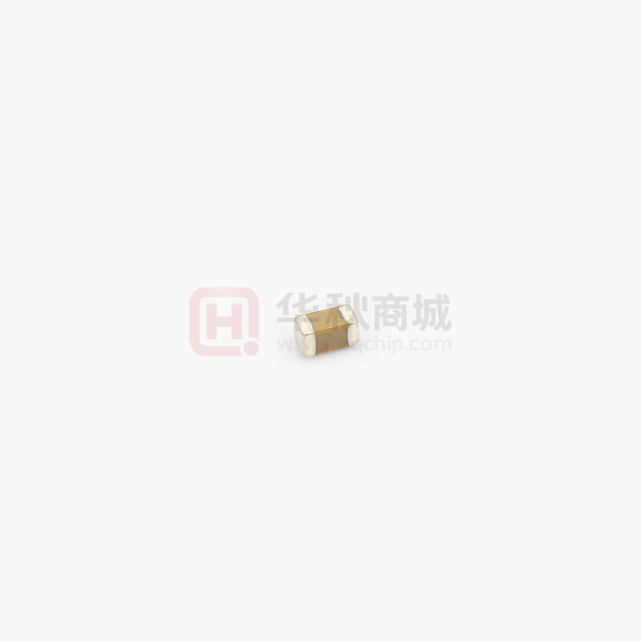
Chip Monolithic Ceramic Capacitor for General
GRM1885C1H182JA01_ (0603, C0G:EIA, 1800pF, DC50V)
_: packaging code
Reference Sheet
1.Scope
This product specification is applied to Chip Monolithic Ceramic Capacitor used for General Electronic equipment.
2.MURATA Part NO. System
(Ex.)
GRM
18
8
(2)T
Dimensions
(1)L/W
Dimensions
5C
1H
(4)Rated
Voltage
(3)Temperature
Characteristics
182
J
(5)Nominal
Capacitance
(6)Capacitance
Tolerance
A01
(7)Murata’s
Control Code
3. Type & Dimensions
(1)-1 L
(1)-2 W
(2) T
e
1.6±0.1
0.8±0.1
0.8±0.1
0.2 to 0.5
(Unit:mm)
g
0.5 min.
4.Rated value
(3) Temperature Characteristics
(Public STD Code):C0G(EIA)
Temp. coeff
Temp. Range
or Cap. Change
(Ref.Temp.)
0±30 ppm/°C
25 to 125 °C
(25 °C)
(4)
Rated
Voltage
DC 50 V
(6)
(5) Nominal
Capacitance
Capacitance
Tolerance
1800 pF
±5 %
Specifications and Test
Methods
(Operating
Temp. Range)
-55 to 125 °C
5.Package
mark
D
J
(8) Packaging
f180mm Reel
PAPER W8P4
f330mm Reel
PAPER W8P4
Packaging Unit
4000 pcs./Reel
10000 pcs./Reel
Product specifications in this catalog are as of Mar.5,2016,and are subject to change or obsolescence without notice.
Please consult the approval sheet before ordering.
Please read rating and !Cautions first.
GRM1885C1H182JA01-01
1
D
(8)Packaging
Code
�■ Specifications and Test Methods
No
1
Item
Rated Voltage
Test Method
(Ref. Standard:JIS C 5101, IEC60384)
Specification
Shown in Rated value.
The rated voltage is defined as the maximum voltage
which may be applied continuously to the capacitor.
When AC voltage is superimposed on DC voltage,
VP-P or VO-P, whichever is larger, should be maintained
within the rated voltage range.
2
Appearance
No defects or abnormalities.
Visual inspection.
3
Dimension
Within the specified dimensions.
Using calipers. (GRM02 size is based on Microscope)
4
Voltage proof
No defects or abnormalities.
Measurement Point
: Between the terminations
Test Voltage
: 300% of the rated voltage
(Temperature compensating type)
250% of the rated voltage
(High dielectric constant type)
Applied Time
: 1s to 5 s
Charge/discharge current : 50mA max.
5
Insulation Resistance(I.R.)
C≦0.047µF:More than 10000MΩ
Measurement Point : Between the terminations
C>0.047µF:More than 500Ω·F
Measurement Voltage :
C:Nominal Capacitance
Charging Time
DC Rated Voltage
: 2 min
Charge/discharge current : 50mA max.
Measurement Temperature : Room Temperature
6
Capacitance
Shown in Rated value.
7
Q
30pF and over:Q≧1000
Measurement Temperature : Room Temperature
Capacitance
C≦1000pF
C>1000pF
30pF and below:Q≧400+20C
Frequency
1.0+/-0.1MHz
1.0+/-0.1kHz
Voltage
0.5 to 5.0Vrms
1.0+/-0.2Vrms
C:Nominal Capacitance(pF)
8
Temperature
No bias
Nominal values of the temperature coefficient is shown in Rated value. The capacitance change should be measured after 5 min
Characteristics
of Capacitance
at each specified temp. stage.
But,the Capacitance Change under 25℃ is shown in Table A.
In case of applying voltage, the capacitance change should be
measured after 1 min with applying voltage in equilibration of
Capacitance Drift
each temp. stage.
Within +/-0.2% or +/-0.05pF
Capacitance value as a reference is the value in step 3.
(Whichever is larger.)
The capacitance drift is calculated by dividing the differences
between the maximum and minimum measured values in the
step 1,3 and 5 by the cap. value in step 3.
Step
1
2
3
4
5
9
Adhesive Strength
No removal of the terminations or other defect
of Termination
should occur.
Temperature(C)
Reference Temp.+/-2
Min. Operating Temp.+/-3
Reference Temp.+/-2
Max. Operating Temp.+/-3
Reference Temp.+/-2
Solder the capacitor on the test substrate shown in Fig.3.
Type
Applied Force(N)
GRM02
1
GRM03
2
GRM15/GRM18
5
GRM21/GRM31/GRM32
Holding Time
10
: 10+/-1s
Applied Direction : In parallel with the test substrate and vertical with
the capacitor side.
JEMCGS-0015S
2
�No
Item
10 Vibration
Test Method
(Ref. Standard:JIS C 5101, IEC60384)
Specification
Appearance
No defects or abnormalities.
Capacitance
Within the specified initial value.
Q
Within the specified initial value.
Solder the capacitor on the test substrate shown in Fig.3.
Kind of Vibration
: A simple harmonic motion
10Hz to 55Hz to 10Hz (1min)
Total amplitude
: 1.5mm
This motion should be applied for a period of 2h in each 3 mutually
perpendicular directions(total of 6h).
11 Substrate
Bending test
Appearance
No defects or abnormalities.
Capacitance
Within +/-5% or +/-0.5pF
Change
(Whichever is larger)
Solder the capacitor on the test substrate shown in Fig.1.
Pressurization method : Shown in Fig.2
: 1mm
Flexure
Holding Time
12 Solderability
95% of the terminations is to be soldered evenly and continuously.
:
5+/-1s
Soldering Method
: Reflow soldering
Test Method
: Solder bath method
Flux
13 Resistance to
Soldering Heat
Solution of rojin ethanol 25(wt)%
Preheat
: 80℃ to 120℃ for 10s to 30s
Solder
: Sn-3.0Ag-0.5Cu
Solder Temp.
: 245+/-5℃
Immersion time
: 2+/-0.5s
Appearance
No defects or abnormalities.
Capacitance
Within +/-2.5% or +/- 0.25pF
Test Method
: Solder bath method
Change
(Whichever is larger)
Solder
: Sn-3.0Ag-0.5Cu
Solder Temp.
: 270+/-5℃
Q
I.R.
Within the specified initial value.
Within the specified initial value.
Immersion time
: 10+/-0.5s
Exposure Time
: 24+/-2h
Preheat
: GRM31 size max.: 120℃ to 150℃ for 1 min
GRM32 size : 100℃ to 120℃ for 1 min
Voltage proof No defects.
and 170℃ to 200℃ for 1 min
14 Temperature
Appearance
No defects or abnormalities.
Sudden Change Capacitance
Change
Within +/-2.5% or+/- 0.25pF
Test Method
: Reflow soldering (hot plate)
Solder
: Sn-3.0Ag-0.5Cu
Solder Temp.
: 270+/-5℃
Reflow Time
: 10+/-0.5s
Test Substrate
: Glass epoxy PCB
Exposure Time
: 24+/-2h
Preheat
: 120℃ to 150℃ for 1 min
Solder the capacitor on the test substrate shown in Fig.3.
(Whichever is larger)
Perform the five cycles according to the four heat treatments
shown in the following table.
Q
I.R.
Within the specified initial value.
Within the specified initial value.
Voltage proof No defects.
Step
Temp.(C)
Time (min)
1
Min.Operating Temp.+0/-3
30+/-3
2
Room Temp.
2 to 3
3
Max.Operating Temp.+3/-0
30+/-3
4
Room Temp
2 to 3
Exposure Time
JEMCGS-0015S
3
: 24+/-2h
�No
Item
15 High
Test Method
(Ref. Standard:JIS C 5101, IEC60384)
Specification
Appearance
No defects or abnormalities.
Solder the capacitor on the test substrate shown in Fig.3.
High Humidity
Capacitance
Within +/-7.5% or +/-0.75pF
Test Temperature
: 40+/-2℃
(Steady)
Change
(Whichever is larger)
Test Humidity
: 90%RH to 95%RH
Temperature
Test Time
Q
: 500+/-12h
30pF and over:Q≧200
Applied Voltage
30pF and below :Q≧100+10C/3
Charge/discharge current : 50mA max.
Exposure Time
: DC Rated Voltage
: 24+/-2h
C:Nominal Capacitance(pF)
16 Durability
I.R.
More than 500MΩ or 25Ω·F (Whichever is smaller)
Appearance
No defects or abnormalities.
Solder the capacitor on the test substrate shown in Fig.3.
Capacitance
Within +/-3% or +/-0.3pF
Test Temperature
Change
(Whichever is larger)
Test Time
Applied Voltage
Q
Charge/discharge current : 50mA max.
10pF and over
Exposure Time
10pF and below : Q≧200+10C
C:Nominal Capacitance (pF)
More than 1,000MΩ or 50Ω·F (Whichever is smaller)
Table A
Char.
5C
6C
6P
6R
6S
6T
7U
-55C
Max.
0.58
0.87
2.33
3.02
4.09
5.46
8.78
JEMCGS-0015S
: 1000+/-12h
: 200% of the rated voltage
30pF and over:Q≧350
30pF and below : Q≧275+5C/2
I.R.
: Max. Operating Temp. +/-3℃
Capacitance Change from 25C
-30C
Min.
Max.
Min.
-0.24
0.40
-0.17
-0.48
0.59
-0.33
0.72
1.61
0.50
1.28
2.08
0.88
2.16
2.81
1.49
3.28
3.75
2.26
5.04
6.04
3.47
(%)
-10C
Max.
0.25
0.38
1.02
1.32
1.79
2.39
3.84
Min.
-0.11
-0.21
0.32
0.56
0.95
1.44
2.21
4
: 24+/-2h
�Substrate Bending test
・Test substrate
Material
: Copper-clad laminated sheets for PCBs
(Glass fabric base, epoxy resin)
Thickness : 1.6mm (GRM02/GRM03/GRM15: t:0.8mm)
Copper foil thickness : 0.035mm
: Solder resist
a
100
*1,2:2.0±0.05
4.0±0.1
Dimension
(mm)
φ1.5 +0.1
b
c *1 *2
-0
0.56
0.23
0.9
0.3
1.5
0.5
A
3.0
1.2
4.0
1.65
0.05以下
5.0
2.0
5.0
2.9
3.5±0.05
40
GRM02
GRM03
GRM15
GRM18
GRM21
GRM31
GRM32
a
0.2
0.3
0.4
1.0
1.2
2.2
2.2
8.0±0.3
Type
c
c
f4.5
B
b
Land
1.75±0.1
(Coat with heat resistant resin for solder)
t
Fig.1
(in mm)
Kind substrate
of Solder : Sn-3.0Ag-0.5Cu
・Test
Pressurization
・Test
substrate method
20
50 min.
Pressurization
speed
1.0mm/s
Pressurize
tor
R5
Flexure:≦1
Support
Capacitance meter
45
45
Fig.2
(in mm)
Adhesive Strength of Termination, Vibration, Temperature Sudden Change, Resistance to Soldering Heat (Reflow method)
High Temperature High Humidity(Steady) , Durability
・Test substrate
Material
: Copper-clad laminated sheets for PCBs
(Glass fabric base, epoxy resin)
Thickness : 1.6mm or 0.8mm
Copper foil thickness : 0.035mm
Kind substrate
of Solder : Sn-3.0Ag-0.5Cu
・Test
Landsubstrate
Dimensions
・Test
Chip Capacitor
Type
Land
c
GRM02
GRM03
GRM15
GRM18
GRM21
GRM31
GRM32
b
a
Solder Resist
a
0.2
0.3
0.4
1.0
1.2
2.2
2.2
Fig.3
JEMCGS-0015S
5
Dimension (mm)
b
0.56
0.9
1.5
3.0
4.0
5.0
5.0
c
0.23
0.3
0.5
1.2
1.65
2.0
2.9
�Package
GRM Type
1.Tape Carrier Packaging(Packaging Code:D/E/W/L/J/F/K)
1.1 Minimum Quantity(pcs./reel)
φ180mm reel
Paper Tape
Plastic Tape
Type
Code:D/E
Code:W
Code:L
GRM01
GRM02
40000(W4P1)
15000(W8P2)
15000(W8P2) 30000(W8P1)
10000(W8P2)
20000(W8P2)
10000(W8P2)
50000(W8P2)
50000(W8P2)
50000(W8P2)
50000(W8P2)
50000(W8P2)
5(LWT Dimensions Tolerance:±0.05)
10000(W8P2) 20000(W8P1)
50000(W8P2)
5(LWT Dimensions Tolerance:±0.1min.)
10000(W8P2)
40000(W8P2)
5 (LW Dimensions Tolerance:±0.1min.
and T Dimensions Tolerance:±0.05)
10000(W8P2)
50000(W8P2)
5(LW Dimensions Tolerance:±0.2
and T Dimensions:0.5 +0/-0.1)
10000(W8P2)
GRM18
GRM31
GRM32
GRM43
GRM55
4000
4000
4000
6
9
A/B
6/9
M/X
C
9
A/M
N
C
R/D/E
M
N/R/D
E
S
M
N/C/R/D
E
F
3000
3000
4000
10000
10000
10000
10000
10000
10000
3000
2000
4000
10000
6000
10000
3000
2000
2000
1000
1000
1000
500
500
1000
1000
500
300
1.2 Dimensions of Tape
(1)GRM01/02 (W4P1 CODE:L)
*1,2:1.0±0.02
*1
*2
1.8±0.02
φ0.8±0.04
2.0±0.04
B
A
10000
8000
6000
4000
5000
4000
2000
1500
5000
4000
1500
(in:mm)
2.0±
* 1,2:1.0± 0.02
*1
0.15~0.25
φ 0.8±0.04
A
B
GRM21
Code:K
2
3
5
2
3/X
4.0±0.05
GRM15
Code:J/ F
50000(W4P1)
0.9±0.05
GRM03
φ330mm reel
Paper Tape Plastic Tape
0.05以下
0.05 max.
t
Type
GRM01
1
GRM02
2
Dimensions(Chip)
L
W
T
0.25±0.013 0.125±0.013 0.125±0.013
0.4±0.02
0.2±0.02
0.2±0.02
0.4±0.05
0.2±0.05
0.2±0.05
JEMCGP-01796E
A *3
0.145
0.23
0.26
*3 Nominal value
6
B *3
t
0.27
0.43
0.46
0.4 max.
0.5 max.
�Package
GRM Type
(2)GRM03/15(W8P2 CODE:D/E/J/F)
*1,2:2.0±0.05
Type
L
2
GRM03
3
5
2
X
3
GRM15
5
0.6±0.03
0.6±0.05
0.6±0.09
1.0±0.05
(in:mm)
Dimensions(Chip)
W
T
0.2 +0.02/-0.04
0.3±0.03
0.3±0.03
0.3±0.05
0.3±0.05
0.3±0.09
0.3±0.09
0.5±0.05
0.2 +0.02/-0.04
0.5±0.05
0.25±0.05
1.0±0.2
1.0±0.05
1.0±0.07
1.0±0.1
1.0±0.15
0.5±0.2
0.5±0.05
0.5±0.07
0.5±0.1
0.5±0.15
1.0±0.2
0.5±0.2
0.3±0.03
0.5±0.05
0.5±0.07
0.5±0.1
0.5±0.15
0.5 +0/-0.1
0.5±0.2
0.5±0.05
A *3
B *3
0.37
0.67
0.39
0.69
0.44
0.74
0.65
1.15
0.78
1.29
0.65
1.15
0.70
0.72
1.20
1.25
0.78
1.29
t
0.5 max.
0.6 max.
0.8 max.
*3 Nominal value
(3)GRM033/155(W8P1 CODE:W)
Type
GRM03
GRM15
3
5
JEMCGP-01796E
L
0.6±0.03
0.6±0.05
0.6±0.09
1.0±0.05
Dimensions(Chip)
W
0.3±0.03
0.3±0.05
0.3±0.09
0.5±0.05
(in:mm)
T
0.3±0.03
0.3±0.05
0.3±0.09
0.5±0.05
7
A *3
0.37
0.39
0.44
0.65
*3 Nominal value
B *3
0.67
0.69
0.74
1.15
t
0.5 max.
0.6 max.
0.8 max.
�
很抱歉,暂时无法提供与“GRM188C71A475KE11D”相匹配的价格&库存,您可以联系我们找货
免费人工找货- 国内价格
- 20+0.23873
- 200+0.22271
- 500+0.20669
- 1000+0.19067
- 3000+0.18266
- 6000+0.17144


 工商网监
湘ICP备2023018690号
工商网监
湘ICP备2023018690号
