Preliminary Specification Number : SP-ZZ1MD-J
WiFi / Bluetooth Module Data Sheet
Cypress CYW43438 WLAN / BT + ST Micro STM32F412 MCU
for 802.11b/g/n & Bluetooth® 4.1
Electric Imp P/N : imp004m
MURATA P/N : LBEE5ZZ1MD-011
This Datasheet is preliminary version, and subject
to change without notice.
Preliminary
< Specification may be changed by Murata without notice >
Murata Manufacturing Co., Ltd.
�Preliminary Specification Number : SP-ZZ1MD-J
1 / 34
Revision history
Issued
Date
Revision
Code
Revision
Page
Jul. 6. 2016
Sep. 9. 2016
A
Oct. 11. 2016
B
Oct. 13. 2016
C
P3
P4
P6
P15
P17
P3
P4
P6
P10
P12
P6
P8
P9
P10
P11
Changed Items
First Issue
2. Part Number
4.1. Dimensions
4.2. Terminal Configurations
11. Land pattern (Top View)
13. Tape and Reel Packing
2. Part Number
4.1. Dimensions (LMK)
42 Terminal Configurations
8. Power up sequence
9. RF Characteristics
4.2. Pin configurations
4.3. Pin mux table
5. LED drive
6. Phototransistor
7. SPI flash requirements
9. Operating condition
10. External 32kHz crystal
14. Reference circuit
15. Recommended components
6. Phototransistor
1. Scope
Oct. 20. 2016
Oct. 21. 2016
D
E
P16
P17
P10
P3
Mar. 14. 2017
F
P5
4.1. Dimensions
P5
Change Reason
Correct imp003 reference
Update cloud information
Correct
Pin 1 Marking
Correct Top view design
Apr. 13. 2017
G
P12
4. Dimensions, Marking and
Terminal Configurations
9. Operating Condition
Apr. 20. 2017
Jun. 27. 2017
H
I
P5
P3
P1
4.1. Dimensions
1. Scope
Part number
P15
7. SPI flash requirements
Added SPI commands
P16
Added Bluetooth
connections
P23
8. Required wiring for Bluetooth
operation
15. Reference circuit
P17
9. Absolute Maximum Rating
Correction
P24
16.3 Flash memory
Updated part number
recommendations
P34
20. Regulatory Requirements
Added FCC and IC
regulations for modular
certification
Jul. 29. 2017
Correct the range of
VDD_WLAN, VDDA_MCU
and VDD_IO_MCU
Correct the marking.
Wording
Updated from temp to
production part number
J
Preliminary
< Specification may be changed by Murata without notice >
Murata Manufacturing Co., Ltd.
�Preliminary Specification Number : SP-ZZ1MD-J
2 / 34
TABLE OF CONTENTS
1. Scope ............................................................................................................................... 3
2. Part Number ..................................................................................................................... 4
3. Block Diagram .................................................................................................................. 5
4. Dimensions, Marking and Terminal Configurations .......................................................... 6
4.1. Dimensions ................................................................................................................ 6
4.2. Terminal Configurations ............................................................................................. 9
4.3. Pin Mux table ........................................................................................................... 12
5. LED drive ........................................................................................................................ 13
6. Phototransistor ............................................................................................................... 14
7. SPI flash requirements ................................................................................................... 15
8. Required wiring for Bluetooth operation ......................................................................... 16
9. Absolute Maximum Rating ............................................................................................. 17
10. Operating Condition ..................................................................................................... 17
11. External 32.768 kHz Crystal ......................................................................................... 18
12. Power Up Sequence .................................................................................................... 19
12.1. Without RESET_L control ...................................................................................... 19
12.2. With RESET_L control ........................................................................................... 19
12.3. RESET_L Circuit .................................................................................................... 20
13. Electrical Characteristics .............................................................................................. 21
14. Land pattern (Top View) ............................................................................................... 22
15. Reference Circuit .......................................................................................................... 23
16. Recommended Components ........................................................................................ 23
16.1. Bi-color LED ........................................................................................................... 23
16.2. Phototransistor ....................................................................................................... 24
16.3. SPI Flash ............................................................................................................... 24
17. Tape and Reel Packing ................................................................................................ 25
18. NOTICE ........................................................................................................................ 28
18.1. Storage Conditions: ............................................................................................... 28
18.2. Handling Conditions: .............................................................................................. 28
18.3. Standard PCB Design (Land Pattern and Dimensions): ........................................ 28
18.4. Notice for Chip Placer: ........................................................................................... 29
18.5. Soldering Conditions: ............................................................................................. 30
18.6. Cleaning: ................................................................................................................ 30
18.7. Operational Environment Conditions: .................................................................... 30
18.8. Input Power Capacity: ............................................................................................ 31
19. PRECONDITION TO USE OUR PRODUCTS ............................................................. 32
20. Regulatory requirements .............................................................................................. 33
20.1. FCC Warning Notice .............................................................................................. 33
20.2. IC Warning Notice .................................................................................................. 34
Please be aware that an important notice concerning availability, standard warranty and
use in critical applications of Murata products and disclaimers thereto appears at the end of
this specification sheet.
Preliminary
< Specification may be changed by Murata without notice >
Murata Manufacturing Co., Ltd.
�Preliminary Specification Number : SP-ZZ1MD-J
3 / 34
1. Scope
This specification is for the LBEE5ZZ1MD (imp004m) module that provides connectivity
to the internet via WiFi. The fully maintained, secure OS that is part of the Electric Imp
cloud service comes pre-loaded.
•
802.11 b/g/n 1x1 WiFi
802.11b 17dBm (typ.)
802.11g 13dBm (typ.)
802.11n 12dBm (typ.) [20MHz channels]
RX Sensitivity -98dBm (typ.) [@1Mbps]
On-board antenna
Supports WEP, WPA, WPA2, WPS
•
Bluetooth 4.1
BTLE support for WiFi configuration using GATT
Automatically shares antenna with WiFi
Optional: requires 4 MCU pins and stack license fee to enable functionality
in commercial products
•
32-bit Cortex M4 processor
- Robust embedded operating system with fail-safe firmware updates
- Virtual machine for customer firmware
- 256kB of application bytecode flash
- Over 190kB of free application RAM
•
Electric Imp OS & service
- Robust embedded operating system with fail-safe, secure OS &
Application updates
- Pre-provisioned MAC address & per-device secrets
- TLS1.2-RSA-ECDHE (forward secrecy) connection to cloud
- Elliptic curve challenge-response to prevent device impersonation
- Fully featured cloud VM for every device for easy integration with
RESTful APIs
- Open source integrations with AWS, Azure, etc services
•
LED drive for red/green status LEDs
•
Phototransistor input for Electric imp’s patented BlinkUpTM technology for easy
configuration from any smartphone, tablet, or web browser
•
18 user selectable I/Os
- GPIO, PWM, Analog input, SPI, UART, I2C
- Dedicated SPI bus for local storage
•
Low power 14uA (typ.) sleep mode
- Option for coin cell RTC battery backup
•
Compliant with the RoHS directive
Preliminary
< Specification may be changed by Murata without notice >
Murata Manufacturing Co., Ltd.
�Preliminary Specification Number : SP-ZZ1MD-J
4 / 34
2. Part Number
Sample Part Number
LBEE5ZZ1MD-TEMP
Production Part Number
LBEE5ZZ1MD-011
Preliminary
< Specification may be changed by Murata without notice >
Murata Manufacturing Co., Ltd.
�Preliminary Specification Number : SP-ZZ1MD-J
5 / 34
3. Block Diagram
Note: 32.768KHz outside of module
Preliminary
< Specification may be changed by Murata without notice >
Murata Manufacturing Co., Ltd.
�Preliminary Specification Number : SP-ZZ1MD-J
6 / 34
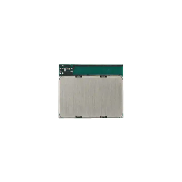
4. Dimensions, Marking and Terminal Configurations
4.1. Dimensions
< Top View >
(H)
(G)
R 001-P01018
FCC:VPYLB1MDIMP004
IC :772C-LB1MDIMP004
(I)
(J)
Model:Type1MD
(D)
imp004m XXXXXXXXX
(E)
(F)
electricimp
(A)
(B)
< Top View >
(C)
< Side View
>
Preliminary
< Specification may be changed by Murata without notice >
Murata Manufacturing Co., Ltd.
�Mark
L
a1
b2
e1
e4
e7
m3
Dimensions
21.0 +/- 0.2
0.4 +/- 0.1
0.2 +/- 0.2
0.3 +/- 0.1
1.6 +/- 0.1
2.5 +/- 0.1
0.7 +/- 0.1
Marking
Marking
(A)
(B)
(C)
(D)
(E)
(F)
(G)
(H)
(I)
(J)
Mark
W
a2
c1
e2
e5
m1
m4
Preliminary Specification Number : SP-ZZ1MD-J
7 / 34
Dimensions
Mark
Dimensions
17.5 +/- 0.2
T
2.3 max.
0.4 +/- 0.1
b1
0.2 +/- 0.2
0.8 +/- 0.1
c2
0.8 +/- 0.1
0.3 +/- 0.1
e3
2.2 +/- 0.1
2.1 +/- 0.1
e6
3.1 +/- 0.1
0.8 +/- 0.1
m2
0.8 +/- 0.1
0.8 +/- 0.1
(unit : mm)
Meaning
Pin 1 Marking
Murata Logo
Electric Imp Logo
Murata Module Type
Imp Module Type
Inspection Number
2D code
Japanese Type certification No.
FCC certification ID
IC certification No.
Structure
PCB Trace
Antenna
Metal Case
PWB
Preliminary
< Specification may be changed by Murata without notice >
Murata Manufacturing Co., Ltd.
�Preliminary Specification Number : SP-ZZ1MD-J
8 / 34
Mounting
The module is designed to be mounted on the edge of the board, with the antenna section
hanging off in free space. The antenna is tuned for free space operation. Please see the
design guide on Electric Imp dev center website at http://www.electricimp.com/docs for
more information.
Preliminary
< Specification may be changed by Murata without notice >
Murata Manufacturing Co., Ltd.
�Preliminary Specification Number : SP-ZZ1MD-J
9 / 34
4.2. Terminal Configurations
Top view (through package)
Preliminary
< Specification may be changed by Murata without notice >
Murata Manufacturing Co., Ltd.
�No.
1
Name
GND
Type
GND
2
CLK_REQ
O
3
BT_REG_ON
I
4
5
6
7
NC
pinM
pinN
pinP
I/O
I/O
I/O
8
pinW
I/O
9
GND
GND
10
pinA
I/O
11
12
pinB
pinC
I/O
I/O
13
LPO_IN
14
15
16
17
18
19
20
21
22
23
24
25
26
pinD
pinE
pinK
pinL
GND
VDD_IO_MCU
GND
pinQ
pinR
pinS
PSU_ENABLE
pinF
pinG
27
pinH
I/O
28
pinJ
I/O
29
30
31
32
33
34
35
36
GND
LED_RED
LED_GREEN
OPTO_IN
OPTO_BIAS
FLASH_MOSI
FLASH_SCLK
FLASH_CS_L
I
I/O
I/O
I/O
I/O
GND
PWR
GND
I/O
I/O
I/O
O
I/O
I/O
GND
O
O
I
O
O
O
O
Preliminary Specification Number : SP-ZZ1MD-J
10 / 34
Description
Reference clock request. As the clock is internal, this pin
does not need to be connected
Enable Bluetooth power. Leave NC if Bluetooth is not
used (active high)
No Connect
GPIO, i2cNM SDA, PWM
GPIO, i2cNM SCL, PWM
GPIO, i2cQP SDA, PWM, IRQ
GPIO, uartBCAW CTS, ADC, IRQ & wake from
deep sleep (active high)
GPIO, uartBCAW RTS, spiAHSR MOSI, ADC,
PWM
GPIO, uartBCAW TX, ADC, PWM, IRQ
GPIO, uartBCAW RX, ADC, IRQ
Sleep Clock (for both WiFi & Bluetooth). If low
power WiFi operation – or Bluetooth operation – is
required, this pin should be connected to pinE.
Otherwise, ground this pin.
GPIO, ADC, PWM, IRQ
GPIO, IRQ
GPIO, spiGJKL SCLK, ADC, PWM
GPIO, spiGJKL NSS, ADC, IRQ
MCU/WLAN VIO
GPIO, uartQ TX, i2cQP SCL, IRQ
GPIO, spiAHSR NSS, IRQ
GPIO, spiAHSR SCLK, IRQ
Active high when WiFi needs 2.7v+
GPIO, uartFGJH TX
GPIO, uartFGJH RX, spiGJKL MOSI
GPIO, uartFGJH CTS, uartHJ TX, spiAHSR MISO,
IRQ
GPIO, uartFGJH RTS, uartHJ RX, spiGJKL MISO,
pulse counter
Red LED drive
Green LED drive
Phototransistor input
Phototransistor supply
SPI flash connection
SPI flash connection
SPI flash connection
Preliminary
< Specification may be changed by Murata without notice >
Murata Manufacturing Co., Ltd.
�37
38
39
40
41
42
43
44
45
46
FLASH_MISO
NC
RESET_L
VSSA/VREFOSC32_OUT
OSC32_IN
GND
VBAT_MCU
VDDA_MCU
VDD_WLAN
I
I
GND
O
I
GND
PWR
PWR
PWR
47-70
GND
GND
71
72
73
74
75-76
BT_UART_TXD
BT_UART_RTS
BT_UART_RXD
BT_UART_CTS
GND
O
O
I
I
GND
77
78-81
82
BT_HOST_WAKE
O
NC
-
BT_DEV_WAKE
I
83
NC
84-103 GND
104
NC
GND
-
Preliminary Specification Number : SP-ZZ1MD-J
11 / 34
SPI flash connection
MCU reset, internally pulled up
Must be connected to GND
32kHz xtal connection
32kHz xtal connection (ground if no xtal fitted)
MCU VBAT input
MCU VDDA input
WLAN VBAT input
Bluetooth UART transmit. Leave NC if not used
Bluetooth UART ready to send. Leave NC if not used
Bluetooth UART receive. Leave NC if not used
Bluetooth UART clear to send. Leave NC if not used
Signal to wake host (from Bluetooth core). Leave NC if not
used
Signal to wake Bluetooth core (from host). Leave NC if not
used
No Connect
Note this pad should not be touching any PCB
Preliminary
< Specification may be changed by Murata without notice >
Murata Manufacturing Co., Ltd.
�Preliminary Specification Number : SP-ZZ1MD-J
12 / 34
4.3. Pin Mux table
Pin
pinA
pinB
pinC
pinD
pinE
pinF
pinG
pinH
pinJ
pinK
pinL
pinM
pinN
pinP
pinQ
pinR
pinS
pinW
Uart
BCAW
RTS
TX
RX
uart
FGJH
TX
RX
CTS
RTS
uart
HJ
uart
Q
i2c
NM
i2c
QP
spi
AHSR
MOSI
spi
GJKL
ADC
PWM
Yes
Yes
Yes
Yes
Yes
Yes
State
change
Yes
Yes
Yes
Yes
Yes
MOSI
TX
RX
MISO
Yes
MISO
SCLK
NSS
Yes
Yes
Yes
SDA
SCL
TX
Yes
Yes
Yes
Yes
Yes
SDA
SCL
NSS
SCLK
CTS
Pulse
count
Yes
Preliminary
< Specification may be changed by Murata without notice >
Murata Manufacturing Co., Ltd.
Yes
Yes
Yes
Yes
Yes
�Preliminary Specification Number : SP-ZZ1MD-J
13 / 34
5. LED drive
The indicator LED should be bicolor, because red, green and amber (red+green) are used
to indicate status.
The LED drive pins will auto-detect common anode or common cathode parts. The
detection is done by looking to see which way up the LED_RED pin is idling at boot; to
ensure this works correctly, please place a 10k resistor in parallel with the red LED.
The current drive on these pins is 20mA maximum.
Please refer to section 15 for the recommended LEDs.
Two specific LED codes indicate errors when talking to the SPI flash:
SPI flash not found
SPI flash error
If you encounter either of these codes, then this indicates an electrical connection issue or
an incompatible flash part.
Preliminary
< Specification may be changed by Murata without notice >
Murata Manufacturing Co., Ltd.
�Preliminary Specification Number : SP-ZZ1MD-J
14 / 34
6. Phototransistor
The phototransistor is used to receive BlinkUp configuration data. The bias resistor
connected between OPTO_IN and GND may need to be adjusted to ensure adequate
sensitivity and response time - in general you need at least 500mV swing on the OPTO_IN
pin between black and white states, with the worst (dimmest) BlinkUp sender you can find.
More information and sample code to tune blinkup is available on the Electric Imp dev
center website.
End-user BlinkUp send data at between 30 and 60 bits per second, depending on the
user’s device. For factory configuration, data is typically sent at 142 bits per second using
red LED(s) in a test fixture. If your application does not require optical configuration, config
can be sent electrically at 142 bits per second from another micro using the OPTO_IN pin.
Please contact us for more details.
It is also recommended to place 0402, 13pF capacitor footprints (Murata
GRM1555C1H130JA01) close to the imp004m between OPTO_BIAS and GND, and
OPTO_IN and GND. If issues are seen with RF coupling onto the blinkup circuit, then these
components will address the issue by presenting a low impedance in the 2.4GHz band.
Please refer to paragraph 15 for the recommended phototransistors.
Preliminary
< Specification may be changed by Murata without notice >
Murata Manufacturing Co., Ltd.
�Preliminary Specification Number : SP-ZZ1MD-J
15 / 34
7. SPI flash requirements
An external SPI Flash part is required for operation, which must be pre-loaded with the
correct WiFi firmware image before assembly. The required image is available from the
Electric Imp dev center website at http://www.electricimp.com/docs
The minimum size of the SPI Flash is 8Mbit (1MB), and the maximum size is 128Mbit
(16MB). The area below address 0xC2000 (776kB) is the pre-programmed area. The
remainder of the flash device is made available to user code programmatically, and may
optionally be pre-programmed for user applications before assembly.
The imp004m’s SPI flash chip must support both 4KB erases (Command 0x20) and 64KB
erases (command 0xD8) and Page Program (command 0x02). You must also ensure that
the SPI flash you use is able to run down to the minimum operational voltage of your
product to ensure that the SPI flash is operational at all times that the imp is operational.
This is critical during upgrades in low battery states. If you are running from a single
LiMnO2 cell (eg. CR123), you should use a wide voltage range SPI flash that is operational
from 1.7-3.6V such as the Macronix MX25R8035FM2IH0.
Minimum Size
8 Mbit (1024 kByte)
Reserved for OS (do not pre-program)
0x000000 to 0xC2000 (776 kByte)
Summary of required SPI flash commands
Required Command
4KB Sector Erase
64KB Block Erase
Page Program
Command in Hex
0x20
0xD8
0x02
Preliminary
< Specification may be changed by Murata without notice >
Murata Manufacturing Co., Ltd.
�Preliminary Specification Number : SP-ZZ1MD-J
16 / 34
8. Required wiring for Bluetooth operation
If Bluetooth is not used in the application, leave all Bluetooth pins (3, 71-74, 77, 82)
unconnected.
To use Bluetooth in an application, you must connect the MCU pins to the Bluetooth device:
•
•
•
•
•
BT_UART_TXD should be connected to an MCU UART RX pin (pinC, pinG or pinJ)
BT_UART_RXD should be connected to the same UART’s TX pin (pinB, pinF or
pinH)
pinE MUST be connected to the LPO in pin, to supply a 32kHz clock to the Bluetooth
radio
BT_REG_ON should be connected to any free MCU pin, to control Bluetooth power
BT_UART_CTS should be grounded (The imp Bluetooth stack uses 2 wire UART)
Aside from pinE, which cannot be reassigned, choice of UART and control pin for
BT_REG_ON is determined by the application – this allows flexibility in complex IO
configurations.
Please refer to the Electric Imp dev center for more information on how to configure the
Bluetooth stack, which is present from impOS release 40.
Note that though use of Bluetooth is free for developers, commercial use incurs an
additional licensing fee for the stack. Please contact sales@electricimp.com for more
details.
Preliminary
< Specification may be changed by Murata without notice >
Murata Manufacturing Co., Ltd.
�Preliminary Specification Number : SP-ZZ1MD-J
17 / 34
9. Absolute Maximum Rating
Storage Temperature
VBAT_MCU
VDDA_MCU
Supply Voltage
VDD_WLAN
VDD_IO_MCU
min.
-40
-0.3
-0.3
-0.5
-0.3
max.
85
4
4
6
3.63
unit
deg.C
V
Stresses in excess of the absolute ratings may cause permanent damage. Functional operation is not implied under
these conditions. Exposure to absolute ratings for extended periods of time may adversely affect reliability. No
damage assuming only one parameter is set at limit at a time with all other parameters is set within operating
condition.
10. Operating Condition
min.
typ.
max.
unit
Operating Temperature Range
-30
25
70
deg.C
Specification Temperature Range
-20
25
55
deg.C
1.65
3.6
VBAT_MCU
3.3
VDDA_MCU
1.8
3.3
3.6
Supply Voltage
V
VDD_WLAN
3.0
3.3
3.6
VDD_IO_MCU
1.8
3.3
3.6
Notes :
n All RF characteristics in this datasheet are defined by Specification Temperature
Range. Specifications require derating at extreme temperatures.
n VDDA_MCU and VDD_IO_MCU must be the same potential.
Preliminary
< Specification may be changed by Murata without notice >
Murata Manufacturing Co., Ltd.
�Preliminary Specification Number : SP-ZZ1MD-J
18 / 34
11. External 32.768 kHz Crystal
If the application requires the imp004m to enter deep sleep mode, a 32kHz crystal should
be attached to the OSC32_IN and OSC32_OUT pins. Please refer to the STM32F412
datasheet and application note AN2867 by STMicroelectronics NV for detailed crystal
requirements.
If deep sleep mode is not required, OSC32_IN should be connected to GND and
OSC32_OUT left floating. The imp004m will detect this state and disable the sleep APIs.
Preliminary
< Specification may be changed by Murata without notice >
Murata Manufacturing Co., Ltd.
�Preliminary Specification Number : SP-ZZ1MD-J
19 / 34
12. Power Up Sequence
12.1. Without RESET_L control
Following timing diagram explain module power up sequence.
Ramp time 90% > 40µs
VBAT_MCU
Timing same as VBAT_MCU
VDDA_MCU
Timing same as VBAT_MCU
VDD_WLAN
Timing same as VBAT_MCU
VDD_IO_MCU
*Power down sequence is opposite sequence of power up.
12.2. With RESET_L control
Ramp time 90% > 40µs
VBAT_MCU
Timing same as VBAT_MCU
VDDA_MCU
Timing same as VBAT_MCU
VDD_WLAN
Timing same as VBAT_MCU
VDD_IO_MCU
RESET_L
Timing of deassertioRESET_L signal same as VDD_IO
*Power down sequence is opposite sequence of power up.
*RESET_L pin must be controlled by Open Drain.
Preliminary
< Specification may be changed by Murata without notice >
Murata Manufacturing Co., Ltd.
�Preliminary Specification Number : SP-ZZ1MD-J
20 / 34
12.3. RESET_L Circuit
VDD_IO_MCU
External
Reset circuit (1)
RESET_L
(3)
40k
(2)
Filter
Internal
Reset
0.1uF
Murata
Module
(1) The reset network protects the device against parasitic resets.
(2) The use must ensure that the level on the RESET_L pin can go below the VIL(NRST) max level
specified in below table. Otherwise the reset is not taken into account by the device.
(3) RESET_L pin must be controlled by Open Drain. High signal must not input to this pin.
Symbol
VIL
Parameter
RESET_L I/O
input low level
voltage
Min
Typ
Max
Unit
-
-
0.1xVDD_IO_MCU+0.1
V
Preliminary
< Specification may be changed by Murata without notice >
Murata Manufacturing Co., Ltd.
�Preliminary Specification Number : SP-ZZ1MD-J
21 / 34
13. Electrical Characteristics
- DC Characteristics 1. DC current
min.
typ.
max.
unit
1) Tx mode1)
300
370
mA
2) Rx mode
45
100
mA
1) Conditions: 25deg.C, VDD_WLAN=3.3V, VDD_IO_MCU=3.3V
(1Mbps mode unless otherwise specified.)
Note: The above mentioned values have been obtained according to our own measuring
methods and may very depend on the circuit, in which the component is actually
incorporated. Therefore, you are kindly requested to test the performance of the
component actually in your set.
Preliminary
< Specification may be changed by Murata without notice >
Murata Manufacturing Co., Ltd.
�Preliminary Specification Number : SP-ZZ1MD-J
22 / 34
14. Land pattern (Top View)
Unit : mm
Preliminary
< Specification may be changed by Murata without notice >
Murata Manufacturing Co., Ltd.
�Preliminary Specification Number : SP-ZZ1MD-J
23 / 34
15. Reference Circuit
16. Recommended Components
16.1. Bi-color LED
Manufacturer
Manufacturer’s part number
SunLED
Liteon
SunLED
Bivar
XZMDKVG59W-1
LTST-C195KGJRKT
XZMDKVG88W
SM1204BC
SunLED
Liteon
XLMDKVG34M
LTL1BEKVJNN
Surface mount
top-view
side-view
Through-hole
3mm
Preliminary
< Specification may be changed by Murata without notice >
Murata Manufacturing Co., Ltd.
�Preliminary Specification Number : SP-ZZ1MD-J
24 / 34
16.2. Phototransistor
Manufacturer
Manufacturer’s part number
Everlight
Fairchild
SunLED
Everlight
PT17-21C/L41/TR8
KDT00030TR
XZRNI56W-1
PT12-21C/TR8
SunLED
LiteOn
XRNI30W-1
LTR-4206
Manufacturer
Adesto Technologies
Macronix International
Adesto Technologies
Cypress Semiconductor Corp
Adesto Technologies
Cypress Semiconductor Corp
Cypress Semiconductor Corp
Cypress Semiconductor Corp
Manufacturer’s part number
AT25SF081
(1)
MX25R8035F
AT25SF161
(2)
S25FL116K
AT25SF321
(2)
S25FL132K
S25FL064L
(2)
S25FL164K
Surface mount
top-view
side-view
Through-hole
3mm
16.3. SPI Flash
Size
8 Mbit
16 Mbit
32 Mbit
64 Mbit
(1) This device offers a wide operating voltage range
(2) This part is EOL, though inventory may still be available through distributors
Preliminary
< Specification may be changed by Murata without notice >
Murata Manufacturing Co., Ltd.
�Preliminary Specification Number : SP-ZZ1MD-J
25 / 34
17. Tape and Reel Packing
(1) Dimensions of Tape (Plastic tape)
0.1
2.0± 0.15
*1
1.5+0.1/-0.0
0.3± 0.05
22.00±0.10
*2
20.2
0.1
.
40.4
0.3
44.0
0.1
1.75
4 .0± 0.1
24.0± 0.1
2.0+0.1/-0.0
18.00± 0.10
2.55±0.1
*1 Cumulative tolerance of max. ± 0.3 every 10 pitches
*2 Reference value
(Unit :
mm)
(2) Dimensions of Reel
45.5
(f 330)
(f 100)
2.0±0.5
f 21±0.8
50.5max
(Unit: mm)
Preliminary
< Specification may be changed by Murata without notice >
Murata Manufacturing Co., Ltd.
�Preliminary Specification Number : SP-ZZ1MD-J
26 / 34
(3) Taping Diagrams
[1] Feeding Hole
: As specified in (1)
[2] Hole for chip
: As specified in (1)
[3] Cover tape : 62μm in thickness
[4] Base tape
: As specified in (1)
Feeding
Direction
Chi
p
(4) Leader and Tail tape
Feeding
direction
Tail tape
Components
PreliminaryNo components Leader tape
(No < Specification may be changed by Murata without notice
(Cover
> tape
components)
alone)
Murata Manufacturing 200mm
Co., Ltd.min.
�Preliminary Specification Number : SP-ZZ1MD-J
27 / 34
(5) The tape for chips are wound clockwise, the feeding holes to the right side as the tape
is pulled toward the user.
(6) The cover tape and the base tape are not adhered at no components area for 250mm
min.
(7) Tear off strength against pulling of cover tape : 5N min.
(8) Packaging unit:
500pcs./ reel
(9) Material: Base tape :
Plastic
Reel :
Plastic
Cover tape, cavity tape and reel are made the anti-static processing.
(10) Peeling of force: 1.1N max. in the direction of peeling as shown below.
1.1 N max.
165 to 180 °
Cover tape
Base tape
(11) Packaging (Humidity proof Packing)
Label
Desiccant
Humidity
Indicator
Label
Anti-humidity
Plastic Bag
Tape and reel must be sealed with the anti-humidity plastic bag. The bag contains the
desiccant and the humidity indicator.
Preliminary
< Specification may be changed by Murata without notice >
Murata Manufacturing Co., Ltd.
�Preliminary Specification Number : SP-ZZ1MD-J
28 / 34
18. NOTICE
18.1. Storage Conditions:
Please use this product within 6month after receipt.
- The product shall be stored without opening the packing under the ambient temperature
from 5 to 35deg.C and humidity from 20 to 70%RH.
(Packing materials, in particular, may be deformed at the temperature over 40deg.C.)
- The product left more than 6months after reception, it needs to be confirmed the
solderability before used.
- The product shall be stored in non corrosive gas (Cl2, NH3, SO2, Nox, etc.).
- Any excess mechanical shock including, but not limited to, sticking the packing materials
by sharp object and dropping the product, shall not be applied in order not to damage the
packing materials.
This product is applicable to MSL3 (Based on JEDEC Standard J-STD-020)
- After the packing opened, the product shall be stored at
Murata Manufacturing Co., Ltd.
�Preliminary Specification Number : SP-ZZ1MD-J
33 / 34
20. Regulatory requirements
If the OEM or system integrator incorporates the 1MD module into their final product and
wishes to reuse the 1MD module’s FCC certification, it is the OEM/system integrator’s
responsibility to ensure compliance is met on production units.
20.1. FCC Warning Notice
This device complies with Part 15 of the FCC Rules. Operation is subject to the following
two conditions: (1) this device may not cause harmful interference and (2) this device must
accept any interference received, including interference that may cause undesired
operation.
Information to Be Supplied to the End User by the OEM or Integrator
The following regulatory and safety notices must be published in documentation supplied to
the end user of the product or system incorporating an adapter in compliance with local
regulations. Host system must be labeled with “Contains FCC ID: VPYLB1MDIMP004. This
imp004m module is to be used only for mobile and fixed application. In order to re-use the
imp004m module FCC approvals, the antenna must be installed to provide a separation
distance of at least 20cm from all persons and must not be co-located with any other
antenna or transmitter. If the module is installed with a separation distance of less than
20cm from all person or is co-located or operating in conjunction with any other antenna or
transmitter then additional FCC testing and certification may be required. End-Users must
be provided with transmitter operation conditions for satisfying RF exposure compliance.
OEM integrators must ensure that the end user has no manual instructions to remove or
install the imp004m module.
Preliminary
< Specification may be changed by Murata without notice >
Murata Manufacturing Co., Ltd.
�Preliminary Specification Number : SP-ZZ1MD-J
34 / 34
20.2. IC Warning Notice
This device complies with Industry Canada license-exempt RSS standard(s).
a. Common information Operation is subject to the following two conditions:
1. This device may not cause interference, and
2. This device must accept any interference, including interference that may cause
undesired operation of the device.
Cet appareil est conforme à la norme(normes) RSS exempte de licence d'Industrie Canada
a. Informations communes Son fonctionnement est soumis aux deux conditions suivantes:
1. Ce dispositive ne peut causer des interferences, et
2. Ce dispositive doit accepter toute interference, y compris les interferences qui peuvent
causer un mauvais fonctionnement du dispositive.
Information to Be Supplied to the End User by the OEM or Integrator Modular information
form OEM
Information to be Supplied to the End User by the OEM or Integrator
The following regulatory and safety notices must be published in documentation supplied to
the end user of the product or system incorporating an adapter in compliance with local
regulations. Host system must be labeled with “Contains IC: 772C-LB1MDIMP004” This
imp004m module is to be used only for mobile and fixed application. In order to re-use the
imp004m module IC approvals, the antenna(s) used in this transmitter must be installed to
provide a separation distance of at least 20cm from all persons and must not be co-located
or operating in conjunction with any other antenna or transmitter. If antenna is installed
with a separation distance of less than 20cm from all person or is co-located or operating in
conjunction with any other antenna or transmitter then additional IC testing and certification
may be required. End-Users must be provided with transmitter operation conditions for
satisfying RF exposure compliance.
OEM integrators must ensure that the end user has no manual instructions to remove or
install the imp004m module.
Preliminary
< Specification may be changed by Murata without notice >
Murata Manufacturing Co., Ltd.
�