Reference Only
Spec No. JELF243A-9106F-01
P.1/8
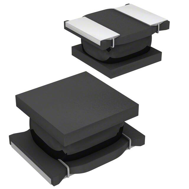
CHIP COIL(CHIP INDUCTORS)LQH32CH□□□□53L
Murata Standard Reference Specification【AEC-Q200】
1.Scope
This Reference specification applies to LQH32CH_53L series, Chip coil (Chip Inductors) for automotive Electronics
based on AEC-Q200.
2.Part Numbering
(ex)
LQ
H
32
C
H
1R0
M
5
3
L
Product ID Structure Dimension Applications Category Inductance Tolerance Features Electrode Packaging
(L×W)
and
L:Taping
Characteristics
3.Rating
Operating Temperature Range.
Storage Temperature Range.
Customer
Part Number
– 40 °C to + 85 °C
– 40 °C to + 105 °C
Inductance
MURATA
Part Number
DC
Resistance
(Ω)
Tolerance
(µH)
Self
Resonant
Frequency
(MHz min)
Rated
Current
(mA)
LQH32CH1R0M53L
1.0
0.060±30%
100
1000
LQH32CH2R2M53L
2.2
0.097±30%
64
790
LQH32CH3R3M53L
3.3
0.12±30%
50
710
LQH32CH4R7M53L
4.7
0.15±30%
43
650
LQH32CH6R8M53L
6.8
0.25±30%
32
540
LQH32CH100K53L
10
0.30±30%
26
450
LQH32CH150K53L
15
0.58±30%
26
300
LQH32CH220K53L
22
0.71±30%
19
250
±20%
±10%
ESD
Rank
5A: 8kV
5A
∗When applied Rated current to the products , self temperature rise shall be limited to 20℃ max and Inductance
will be within ±10% of initial Inductance value.
4. Testing Conditions
《Unless otherwise specified》
Temperature : Ordinary Temperature / 15°C to 35°C
: Ordinary Humidity / 25%(RH) to 85%(RH)
Humidity
《In case of doubt》
Temperature : 20°C± 2°C
Humidity
: 60%(RH) to 70%(RH)
Atmospheric Pressure : 86kPa to 106 kPa
5. Appearance and Dimensions
2.5 ± 0.2
1.55 ± 0.15
2.5 ± 0.2
A
A
2.5 ± 0.2
3.2 ± 0.3
A : 2.8 max.
※ No marking.
0.9 ± 0.31.3 ± 0.2 0.9 ± 0.3
MURATA MFG.CO., LTD
■Unit Mass (Typical value)
0.045g
�Spec No. JELF243A-9106F-01
Reference Only
P.2/8
6. Electrical Performance
No.
6.1
Item
Inductance
Specification
Inductance shall meet item 3.
Test Method
Measuring Equipment :
KEYSIGHT 4192A or equivalent
Measuring Frequency : 1MHz
6.2
DC
Resistance
DC Resistance shall meet item 3.
Measuring Equipment : Digital multi meter
6.3
Self Resonant
Frequency(S.R.F)
S.R.F shall meet item 3.
Measuring Equipment :
KEYSIGHT E4991A or equivalent
7. AEC-Q200 Requirement
7.1 Performance (based on Table 5 for Magnetics(Inductors / Transformer)
AEC-Q200 Rev.D issued June. 1 2010
AEC-Q200
Murata Specification / Deviation
No
Stress
Test Method
Meet Table A after testing.
1000hours at 85 deg C
3 High
Table A
Set for 24hours at room
Temperature
Appearance
No damage
temperature, then measured.
Exposure
Inductance change
Within ±5%
DC Resistance
Within ±5%
Change
4
Temperature
Cycling
1000cycles
-40 deg C to + 85deg C
Set for 24hours at room
temperature,then
measured.
Meet Table A after testing.
7
Biased Humidity
1000hours at 85 deg C,
85%RH
unpowered.
Meet Table A after testing.
8 Operational Life
Apply 85 deg C 1000 hours Meet Table A after testing.
Set for 24hours at room
temperature, then measured
9 External Visual
Visual inspection
No abnormalities
10 Physical
Dimension
Meet ITEM 5
(Style and Dimensions)
No defects
12 Resistance
to Solvents
Per
MIL-STD-202
Method 215
Not Applicable
13 Mechanical Shock Per MIL-STD-202
Method 213
Condition C:
100g’s/6ms/Half sine
14 Vibration
Meet Table A after testing.
5g's for 20 minutes,
No defects
12cycles eah of 3 orientations
Test from 10-2000Hz.
15 Resistance
No-heating
to Soldering Heat Solder temperature
260C+/-5 deg C
Immersion time 10s
Murata deviation request :
Pre-heating: 150C+/-5C, 60s+/-5s
Meet Table A after testing.
MURATA MFG.CO., LTD
�Reference Only
Spec No. JELF243A-9106F-01
AEC-Q200
Test Method
Per AEC-Q200-002
No
Stress
17 ESD
P.3/8
Murata Specification / Deviation
ESD Rank: Refer to Item 3. Rating.
No defects
18 Solderbility
Per J-STD-002
Method b : Not Applicable
90% of the terminations is to be soldered.
(Except exposed wire)
19 Electrical
Characterization
Measured : Inductance
No defects
20 Flammability
Per UL-94
Not Applicable
21 Board Flex
Epoxy-PCB(1.6mm)
Deflection 2mm(min)
60s minimum holding time
Murata deviation request: 30s
No defects
22 Terminal Strength Per AEC-Q200-006
A force of 17.7N for 60s
No defects
3.5±0.05
3.6±0.2
4.0±0.1
2.9±0.2
(0.2)
0.2
※The packing directions of the chip coil
in taping are unified with the in/out
positions of the lead wire.
8.0±0.2
※ Lead- in/out wire
+0.1
φ 1.5 -0
1.75±0.1
8. Specification of Packaging
8.1 Appearance and Dimensions of plastic tape
4.0±0.1
2.0±0.05
1.7±0.2
Direction of feed
Dimension of the Cavity is measured at the bottom side.
8.2 Specification of Taping
(1) Packing quantity (standard quantity)
2,000 pcs / reel
(2) Packing Method
Products shall be packed in the each embossed cavity of plastic tape and sealed by cover tape.
(3) Sprocket hole
The sprocket holes are to the right as the tape is pulled toward the user.
(4) Spliced point
Plastic tape and Cover tape has no spliced point.
(5) Missing components number
Missing components number within 0.1 % of the number per reel or 1 pc., whichever is greater, and
are not continuous. The specified quantity per reel is kept.
8.3 Pull Strength
Embossed carrier tape
10N min.
Cover tape
5N min.
8.4 Peeling off force of cover tape
Speed of Peeling off
Peeling off force
300mm / min
0.2N to 0.7N
(minimum value is typical)
165 to 180 degree
F
Cover tape
Plastic tape
MURATA MFG.CO., LTD
�Reference Only
Spec No. JELF243A-9106F-01
P.4/8
8.5 Dimensions of Leader-tape, Trailer and Reel
There shall be leader-tape (cover tape) and trailer-tape (empty tape) as follows.
Leader
Trailer
2.0±0.5
160 min.
190 min.
Label
Empty tape
210 min.
Cover tape
φ 13.0±0.2
1
φ 60± 0
φ 21.0±0.8
9± 10
Direction of feed
13±1.4
0
φ 180± 3
8.6 Marking for reel
Customer part number, MURATA part number, Inspection number(∗1), RoHS marking(∗2), Quantity etc ・・・
□□ OOOO ×××
∗1)
(1)
(2)
(3)
(1) Factory Code
(2) Date
First digit
Second digit
: Year / Last digit of year
: Month / Jan. to Sep. → 1 to 9, Oct. to Dec. → O, N, D
Third, Fourth digit
: Day
(3) Serial No.
∗2) « Expression of RoHS marking »
ROHS – Y (△)
(1) (2)
(1) RoHS regulation conformity parts.
(2) MURATA classification number
8.7 Marking for Outside package (corrugated paper box)
Customer name, Purchasing order number, Customer part number, MURATA part number,
RoHS marking (∗2) ,Quantity, etc ・・・
8.8. Specification of Outer Case
Label
186
H
D
W
9.
Outer Case Dimensions
(mm)
W
D
H
186
93
Standard Reel Quantity in Outer Case
(Reel)
5
∗Above Outer Case size is typical. It depends on a quantity of an order
Caution
9.1Limitation of Applications
Please contact us before using our products for the applications listed below which require especially high reliability
for the prevention of defects which might directly cause damage to the third party's life, body or property.
(7) Traffic signal equipment
(1) Aircraft equipment
(2) Aerospace equipment
(8) Disaster prevention / crime prevention equipment
(3) Undersea equipment
(9) Data-processing equipment
(4) Power plant control equipment
(10) Applications of similar complexity and /or reliability requirements
(5) Medical equipment
to the applications listed in the above
(6) Transportation equipment (vehicles, trains, ships, etc.)
9.2 Caution(Rating)
Do not exceed maximum rated current of the product. Thermal stress may be transmitted to the product and
short/open circuit of the product or falling off the product may be occurred.
9.3 Fail-safe
Be sure to provide an appropriate fail-safe function on your product to prevent a second damage that may be
caused by the abnormal function or the failure of our product.
MURATA MFG.CO., LTD
�Spec No. JELF243A-9106F-01
Reference Only
P.5/8
10. Notice
This product is designed for solder mounting.
Please consult us in advance for applying other mounting method such as conductive adhesive.
10.1 Land pattern designing
Recommended land patterns for flow and reflow soldering are as follows:
It has been designed for Electric characteristics and solderability.
Please follow the recommended pattern. Otherwise, their performance which includes electrical performance or
solderability may be affected, or result to "position shift" in soldering process.
Reflow Soldering ∗
Flow Soldering
5.5
Land
5.5
Chip Coil
1.0
1.0
2.0
Solder Resist
1.0
1.3
1.3
1.0
(in mm)
∗ Applicable to flow soldering.
10.2 Flux, Solder
Flux
Solder
・Use rosin-based flux.
・Don’t use highly acidic flux with halide content exceeding 0.2(wt)% (chlorine conversion value).
・ Don’t use water-soluble flux.
・Use Sn-3.0Ag-0.5Cu solder
・Standard thickness of solder paste : 200μm to 300μm
Other flux (except above) Please contact us for details, then use.
10.3 Flow soldering / Reflow soldering conditions
Pre-heating should be in such a way that the temperature difference between solder and product surface is
limited to 150°C max. Cooling into solvent after soldering also should be in such a way that the temperature
difference is limited to 100°C max.
Insufficient pre-heating may cause cracks on the product, resulting in the deterioration of products quality.
Standard soldering profile and the limit soldering profile is as follows.
The excessive limit soldering conditions may cause leaching of the electrode and / or resulting in the deterioration
of product quality.
・Soldering profile
(1)Flow soldering profile
Temp.
(℃)
265℃±3℃
250℃
Limit Profile
150
Heating Time
60s min.
Time. (s)
Standard Profile
Pre-heating
Heating
Cycle of flow
Standard Profile
Limit Profile
150℃, 60s min.
250℃, 4s~6s
265℃±3℃, 5s
2 times
1 time
MURATA MFG.CO., LTD
�Spec No. JELF243A-9106F-01
Reference Only
P.6/8
(2)Reflow soldering profile
Temp.
(℃)
260℃
245℃±3℃
230℃
220℃
Limit Profile
180
150
Standard Profile
30s~60s
60s max.
90s±30s
Time. (s)
Standard Profile
150~180°C, 90s±30s
Pre-heating
Heating
Limit Profile
above 220°C, 30s~60s
above 230°C, 60s max.
245±3°C
260°C,10s
2 times
1 time
Peak temperature
Cycle of reflow
10.4 Reworking with soldering iron.
The following conditions must be strictly followed when using a soldering iron.
Pre-heating
150°C,1 min
Tip temperature
350°C max.
Soldering iron output
80W max.
Tip diameter
φ3mm max.
Soldering time
3(+1,-0)s
Times
2 times
Note : Do not directly touch the products with the tip of the soldering iron in order to prevent the crack on
the products due to the thermal shock.
10.5 Solder Volume
Solder shall be used not to be exceeded the upper limits as shown below.
Accordingly increasing the solder volume, the mechanical stress to Chip is also increased.
Exceeding solder volume may cause the failure of mechanical or electrical performance.
Upper Limit
1/3T≦t≦T
T: Lower flange thickness
Recommendable
T
t
10.6 Product’s location
The following shall be considered when designing and laying out P.C.B.'s.
(1) P.C.B. shall be designed so that products are not subject to the mechanical stress due to warping the board.
[Products direction]
a
b
〈 Poor example 〉
Products shall be located in the sideways
direction (Length:a D *1
(2) Add slits in the board separation part.
A
> B
(3) Keep the mounting position of the component away from
the board separation surface.
A
> C
Seam
b
A
C
B
D
Slit
*1 A > D is valid when stress is added vertically to
the perforation as with Hand Separation.
If a Cutting Disc is used, stress will be diagonal to
the PCB, therefore A > D is invalid.
Length:a< b
a
(3) Mounting Components Near Screw Holes
When a component is mounted near a screw hole,
it may be affected by the board deflection that occurs
during the tightening of the screw. Mount the component
in a position as far away from the screw holes as possible.
Screw Hole
Recommended
10.7 Cleaning Conditions
Products shall be cleaned on the following conditions.
(1) Cleaning temperature shall be limited to 60°C max.(40°C max for alcohol type cleaner.)
(2) Ultrasonic cleaning shall comply with the following conditions with avoiding the resonance
phenomenon at the mounted products and P.C.B.
Power : 20 W / l max.
Frequency : 28kHz to 40kHz
Time : 5 min max.
(3) Cleaner
1. Alternative cleaner
Isopropyl alcohol (IPA)
2. Aqueous agent
PINE ALPHA ST-100S
(4) There shall be no residual flux and residual cleaner after cleaning.
In the case of using aqueous agent, products shall be dried completely after rinse with de-ionized water in
order to remove the cleaner.
(5) Other cleaning
Please contact us.
10.8 Resin coating
The inductance value may change due to high cure-stress of resin to be used for coating/molding products.
An open circuit issue may occur by mechanical stress caused by the resin, amount/cured shape of resin, or
operating condition etc. Some resin contains some impurities or chloride possible to generate chlorine by hydrolysis
under some operating condition may cause corrosion of wire of coil, leading to open circuit.
So, please pay your careful attention when you select resin in case of coating/molding the products with the resin.
Prior to use the coating resin, please make sure no reliability issue is observed by evaluating products mounted on
your board.
10.9 Caution for use
Sharp material such as a pair of tweezers or other material such as bristles of cleaning brush, shall not be touched to the
winding portion to prevent the breaking of wire.
Mechanical shock should not be applied to the products mounted on the board to prevent the breaking of the core
10.10 Handling of a substrate
After mounting products on a substrate, do not apply any stress to the product caused by bending or twisting to the
substrate when cropping the substrate, inserting and removing a connector from the substrate or tightening screw to
the substrate.
Excessive mechanical stress may cause cracking in the product.
Bending
Twisting
MURATA MFG.CO., LTD
�Spec No. JELF243A-9106F-01
Reference Only
P.8/8
10.11 Storage and Handing Requirements
(1) Storage period
Use the products within 12 months after delivered.
Solderability should be checked if this period is exceeded.
(2) Storage conditions
Products should be stored in the warehouse on the following conditions.
Temperature : -10 °C to 40 °C
Humidity
: 15 % to 85 % relative humidity No rapid change on temperature and humidity
The electrode of the products is coated with solder. Don't keep products in corrosive gases
such as sulfur,chlorine gas or acid, or it may cause oxidization of electrode, resulting in
poor solderability.
Products should not be stored on bulk packaging condition to prevent the chipping of the core and the
breaking of winding wire caused by the collision between the products.
Products should be stored on the palette for the prevention of the influence from humidity, dust and so on.
Products should be stored in the warehouse without heat shock, vibration, direct sunlight and so on.
(3) Handling Condition
Care should be taken when transporting or handling product to avoid excessive vibration or mechanical shock.
11. Note
(1) Please make sure that your product has been evaluated in view of your specifications with our product being
mounted to your product.
(2) You are requested not to use our product deviating from the agreed specifications.
(3) The contents of this reference specification are subject to change without advance notice. Please approve our
product specifications or transact the approval sheet for product specifications before ordering
MURATA MFG.CO., LTD
�