Spec No.JELF243A-0050AA-01
Reference Only
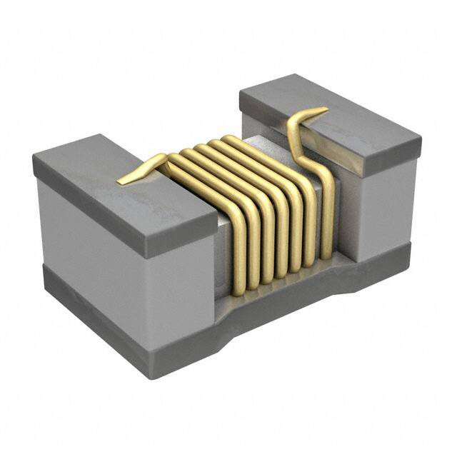
CHIP COIL (CHIP INDUCTORS) LQW15AN□□□□00D
P.1/14
Reference Specification
1.Scope
This Reference Specification applies to LQW15AN_00 series, Chip coil (Chip Inductors).
2.Part Numbering
(ex)
LQ
W
15
A
N
1N5
B
0
0
D
Product ID Structure Dimension Applications Category Inductance Tolerance Features Electrode Packaging
(L×W)
and
D:Taping
Characteristics
*B:Bulk
* Bulk packing also available. (A product is put in the plastic bag under the taping conditions.)
3.Rating
・Operating Temperature Range.
・Storage Temperature Range.
Customer
Part Number
MURATA
Part Number
LQW15AN1N5B00D
LQW15AN1N5C00D
LQW15AN1N5D00D
LQW15AN1N6C00D
LQW15AN1N6D00D
LQW15AN1N7C00D
LQW15AN1N7D00D
LQW15AN1N8C00D
LQW15AN1N8D00D
LQW15AN2N4B00D
LQW15AN2N4C00D
LQW15AN2N4D00D
LQW15AN2N5B00D
LQW15AN2N5C00D
LQW15AN2N5D00D
LQW15AN2N6B00D
LQW15AN2N6C00D
LQW15AN2N6D00D
LQW15AN2N7B00D
LQW15AN2N7C00D
LQW15AN2N7D00D
LQW15AN2N8B00D
LQW15AN2N8C00D
LQW15AN2N8D00D
LQW15AN2N9B00D
LQW15AN2N9C00D
LQW15AN2N9D00D
LQW15AN3N0B00D
LQW15AN3N0C00D
LQW15AN3N0D00D
LQW15AN3N1B00D
LQW15AN3N1C00D
LQW15AN3N1D00D
LQW15AN3N2B00D
LQW15AN3N2C00D
LQW15AN3N2D00D
LQW15AN3N9B00D
LQW15AN3N9C00D
LQW15AN3N9D00D
LQW15AN4N1B00D
LQW15AN4N1C00D
LQW15AN4N1D00D
LQW15AN4N3B00D
LQW15AN4N3C00D
LQW15AN4N3D00D
–55°C ~ +125°C
–55°C ~ +125°C
Inductance
(nH)
Tolerance
1.5
B:±0.1nH
C:±0.2nH
D:±0.5nH
1.6
1.7
Q
(min.)
10
C:±0.2nH
D:±0.5nH
DC
Resistance
(Ω max.)
Self
Resonant
Frequency
(GHz min.)
Rated
Current
(mA)
0.03
18.0
1000
0.07
750
17.0
0.10
1.8
0.16
640
16.0
460
2.4
2.5
0.05
2.6
850
15.0
2.7
20
2.8
2.9
3.0
B:±0.1nH
C:±0.2nH
D:±0.5nH
3.1
0.07
750
0.13
570
14.0
3.2
15
0.17
25
0.07
500
3.9
4.1
4.3
MURATA MFG.CO.,LTD
10.0
750
�Spec No.JELF243A-0050AA-01
Customer
Part Number
Reference Only
MURATA
Part Number
LQW15AN4N4B00D
LQW15AN4N4C00D
LQW15AN4N4D00D
LQW15AN4N5B00D
LQW15AN4N5C00D
LQW15AN4N5D00D
LQW15AN4N6B00D
LQW15AN4N6C00D
LQW15AN4N6D00D
LQW15AN4N7B00D
LQW15AN4N7C00D
LQW15AN4N7D00D
LQW15AN4N8B00D
LQW15AN4N8C00D
LQW15AN4N8D00D
LQW15AN4N9B00D
LQW15AN4N9C00D
LQW15AN4N9D00D
LQW15AN5N0B00D
LQW15AN5N0C00D
LQW15AN5N0D00D
LQW15AN5N1B00D
LQW15AN5N1C00D
LQW15AN5N1D00D
LQW15AN5N8B00D
LQW15AN5N8C00D
LQW15AN5N8D00D
LQW15AN6N2B00D
LQW15AN6N2C00D
LQW15AN6N2D00D
LQW15AN6N3B00D
LQW15AN6N3C00D
LQW15AN6N3D00D
LQW15AN6N4B00D
LQW15AN6N4C00D
LQW15AN6N4D00D
LQW15AN6N5B00D
LQW15AN6N5C00D
LQW15AN6N5D00D
LQW15AN6N6B00D
LQW15AN6N6C00D
LQW15AN6N6D00D
LQW15AN6N7B00D
LQW15AN6N7C00D
LQW15AN6N7D00D
LQW15AN6N8G00D
LQW15AN6N8H00D
LQW15AN6N8J00D
LQW15AN6N9G00D
LQW15AN6N9H00D
LQW15AN6N9J00D
LQW15AN7N0G00D
LQW15AN7N0H00D
LQW15AN7N0J00D
LQW15AN7N1G00D
LQW15AN7N1H00D
LQW15AN7N1J00D
LQW15AN7N2G00D
LQW15AN7N2H00D
LQW15AN7N2J00D
Inductance
(nH)
Tolerance
Q
(min.)
DC
Resistance
(Ω max.)
P.2/14
Self
Resonant
Frequency
(GHz min.)
Rated
Current
(mA)
4.4
4.5
4.6
0.07
750
4.7
4.8
8.0
4.9
5.0
5.1
0.12
600
0.09
700
B:±0.1nH
C:±0.2nH
D:±0.5nH
5.8
6.2
25
6.3
6.4
6.5
6.6
6.7
6.0
6.8
6.9
7.0
G:±2%
H:±3%
J:±5%
7.1
7.2
MURATA MFG.CO.,LTD
0.13
570
�Spec No.JELF243A-0050AA-01
Customer
Part Number
Reference Only
MURATA
Part Number
LQW15AN7N3G00D
LQW15AN7N3H00D
LQW15AN7N3J00D
LQW15AN7N5G00D
LQW15AN7N5H00D
LQW15AN7N5J00D
LQW15AN8N2G00D
LQW15AN8N2H00D
LQW15AN8N2J00D
LQW15AN8N6G00D
LQW15AN8N6H00D
LQW15AN8N6J00D
LQW15AN8N7G00D
LQW15AN8N7H00D
LQW15AN8N7J00D
LQW15AN8N8G00D
LQW15AN8N8H00D
LQW15AN8N8J00D
LQW15AN8N9G00D
LQW15AN8N9H00D
LQW15AN8N9J00D
LQW15AN9N0G00D
LQW15AN9N0H00D
LQW15AN9N0J00D
LQW15AN9N1G00D
LQW15AN9N1H00D
LQW15AN9N1J00D
LQW15AN9N2G00D
LQW15AN9N2H00D
LQW15AN9N2J00D
LQW15AN9N3G00D
LQW15AN9N3H00D
LQW15AN9N3J00D
LQW15AN9N4G00D
LQW15AN9N4H00D
LQW15AN9N4J00D
LQW15AN9N5G00D
LQW15AN9N5H00D
LQW15AN9N5J00D
LQW15AN9N6G00D
LQW15AN9N6H00D
LQW15AN9N6J00D
LQW15AN9N7G00D
LQW15AN9N7H00D
LQW15AN9N7J00D
LQW15AN9N8G00D
LQW15AN9N8H00D
LQW15AN9N8J00D
LQW15AN9N9G00D
LQW15AN9N9H00D
LQW15AN9N9J00D
LQW15AN10NG00D
LQW15AN10NH00D
LQW15AN10NJ00D
LQW15AN11NG00D
LQW15AN11NH00D
LQW15AN11NJ00D
LQW15AN12NG00D
LQW15AN12NH00D
LQW15AN12NJ00D
Inductance
(nH)
Tolerance
Q
(min.)
P.3/14
DC
Resistance
(Ω max.)
Self
Resonant
Frequency
(GHz min.)
Rated
Current
(mA)
0.13
6.0
570
7.3
7.5
8.2
8.6
8.7
8.8
8.9
9.0
9.1
25
9.2
0.14
G:±2%
H:±3%
J:±5%
540
9.3
5.5
9.4
9.5
9.6
9.7
9.8
9.9
10
0.17
500
11
30
12
MURATA MFG.CO.,LTD
0.14
�Spec No.JELF243A-0050AA-01
Customer
Part Number
Reference Only
MURATA
Part Number
LQW15AN13NG00D
LQW15AN13NH00D
LQW15AN13NJ00D
LQW15AN15NG00D
LQW15AN15NH00D
LQW15AN15NJ00D
LQW15AN16NG00D
LQW15AN16NH00D
LQW15AN16NJ00D
LQW15AN18NG00D
LQW15AN18NH00D
LQW15AN18NJ00D
LQW15AN19NG00D
LQW15AN19NH00D
LQW15AN19NJ00D
LQW15AN20NG00D
LQW15AN20NH00D
LQW15AN20NJ00D
LQW15AN22NG00D
LQW15AN22NH00D
LQW15AN22NJ00D
LQW15AN23NG00D
LQW15AN23NH00D
LQW15AN23NJ00D
LQW15AN24NG00D
LQW15AN24NH00D
LQW15AN24NJ00D
LQW15AN27NG00D
LQW15AN27NH00D
LQW15AN27NJ00D
LQW15AN30NG00D
LQW15AN30NH00D
LQW15AN30NJ00D
LQW15AN33NG00D
LQW15AN33NH00D
LQW15AN33NJ00D
LQW15AN36NG00D
LQW15AN36NH00D
LQW15AN36NJ00D
LQW15AN39NG00D
LQW15AN39NH00D
LQW15AN39NJ00D
LQW15AN40NG00D
LQW15AN40NH00D
LQW15AN40NJ00D
LQW15AN43NG00D
LQW15AN43NH00D
LQW15AN43NJ00D
LQW15AN47NG00D
LQW15AN47NH00D
LQW15AN47NJ00D
LQW15AN51NG00D
LQW15AN51NH00D
LQW15AN51NJ00D
LQW15AN56NG00D
LQW15AN56NH00D
LQW15AN56NJ00D
LQW15AN62NG00D
LQW15AN62NH00D
LQW15AN62NJ00D
Inductance
(nH)
Tolerance
13
Q
(min.)
DC
Resistance
(Ω max.)
25
0.21
P.4/14
Self
Resonant
Frequency
(GHz min.)
Rated
Current
(mA)
430
5.0
15
30
16
0.16
460
0.24
18
4.5
370
0.27
19
20
4.0
22
0.30
23
310
3.8
24
27
0.52
3.5
280
0.58
3.3
270
G:±2%
H:±3%
J:±5%
30
25
33
3.2
0.63
36
260
3.1
39
40
0.70
3.0
250
43
47
2.9
1.08
51
2.85
56
62
MURATA MFG.CO.,LTD
210
20
1.17
2.8
200
1.82
2.6
145
�Reference Only
Spec No.JELF243A-0050AA-01
Customer
Part Number
Inductance
MURATA
Part Number
(nH)
LQW15AN68NG00D
LQW15AN68NJ00D
LQW15AN72NG00D
LQW15AN72NJ00D
LQW15AN75NG00D
LQW15AN75NJ00D
LQW15AN82NG00D
LQW15AN82NJ00D
LQW15AN91NG00D
LQW15AN91NJ00D
LQW15ANR10J00D
LQW15ANR12J00D
Tolerance
Q
(min.)
68
DC
Resistance
(Ω max.)
P.5/14
Self
Resonant
Frequency
(GHz min.)
1.96
Rated
Current
(mA)
140
2.5
72
75
2.10
G:±2%
J:±5%
135
2.4
20
82
2.24
2.3
130
91
2.38
2.1
125
2.52
2.66
1.5
1.0
120
110
100
120
J:±5%
4. Testing Conditions
《Unless otherwise specified》
《In case of doubt》
Temperature : Ordinary Temperature / 15°C to 35°C
Temperature : 20°C±2°C
: Ordinary Humidity
/ 25%(RH) to 85%(RH)
Humidity
: 60%(RH) to 70%(RH)
Humidity
Atmospheric Pressure : 86kPa to 106 kPa
5. Appearance and Dimensions
1.0±0.1
W
■Unit mass (Typical value)
0.0008g
0.1±0.05
0.5±0.1
0.5±0.1
0.2±0.1
0.2±0.1
*Dimension of W
Inductance
1N5~23N
24N~R12
(in mm)
W (in mm)
0.6±0.1
0.5±0.1
MURATA MFG.CO.,LTD
�Spec No.JELF243A-0050AA-01
Reference Only
P.6/14
6.Electrical Performance
No.
6.1
Item
Inductance
Specification
Inductance shall meet item 3.
Test Method
Measuring Equipment:
KEYSIGHT E4991A or equivalent
Measuring Frequency:
100MHz
250MHz/ 1.5nH~43nH
200MHz/ 47nH~68nH
150MHz/ 72nH~120nH
Measuring Condition:
Test signal level / about 0dBm
Electrical length / 0.94cm
Measuring Fixture: KEYSIGHT 16193A
Position coil under test as shown in below and
contact coil with each terminal by adding weight.
6.2
Q
Q shall meet item 3.
0.5mm
Measuring Method: See the endnote.
6.3
DC Resistance
DC Resistance shall meet item 3.
Measuring Equipment:Digital multi meter
6.4
Self Resonant
Frequency(S.R.F)
S.R.F shall meet item 3.
Measuring Equipment:KEYSIGHT N5230A
or equivalent
6.5
Rated Current
Self temperature rise shall be
limited to 20°C max.
The rated current is applied.
Specification
Chip coil shall not be damaged
after tested as test method.
Test Method
Substrate:Glass-epoxy substrate
7.Mechanical Performance
No.
7.1
Item
Shear Test
Chip Coil
Pattern
1.2
Solder resist
Substrate
0.65
0.5
Chip Coil
Applied Direction:
(in mm)
F
Substrate
Force:5N
Hold Duration:5s±1s
7.2
Bending Test
Substrate:Glass-epoxy substrate
(100mm×40mm×0.8mm)
Speed of Applying Force:1mm / s
Deflection:2mm
Hold Duration:5s
Pressure jig
R340
F
Deflection
45
MURATA MFG.CO.,LTD
45
Product
(in mm)
�Reference Only
Spec No.JELF243A-0050AA-01
P.7/14
No.
7.3
Item
Vibration
Specification
Chip coil shall not be damaged
after tested as test method.
Test Method
Oscillation Frequency:
10Hz~55Hz~10Hz for 1 min
Total Amplitude:1.5mm
Testing Time:
A period of 2 hours in each of mutually
perpendicular directions.
7.4
Solderability
The wetting area of the electrode
shall be at least 90% covered with
new solder coating.
Flux:Ethanol solution of rosin,25(wt)%
Includes activator equivalent to 0.06(wt)%
chlorine.(immersed for 5s to 10s)
Solder:Sn-3.0Ag-0.5Cu
Pre-Heating:150°C±10°C / 60s to 90s
Solder Temperature:240°C±5°C
Immersion Time:3s±1s
7.5
Resistance to
Soldering Heat
Appearance:No damage
Inductance Change: within ±5%
Flux:Ethanol solution of rosin,25(wt)%
Includes activator equivalent to 0.06(wt)%
Chlorine.(immersed for 5s to 10s)
Solder:Sn-3.0Ag-0.5Cu
Pre-Heating:150°C±10°C / 60s to 90s
Solder Temperature:270°C±5°C
Immersion Time:10s±1s
Then measured after exposure in the room
condition for 24h±2h.
8.Environmental Performance
It shall be soldered on the substrate.
No.
Item
Specification
8.1 Heat Resistance
Appearance:No damage
Inductance Change: within ±5%
Q Change: within ±20%
Test Method
Temperature:125°C±2°C
Time:1000h (+48h,0h)
Then measured after exposure in the room
condition for 24h±2h.
8.2
Cold Resistance
Temperature:-55°C±2°C
Time:1000h (+48h,-0h)
Then measured after exposure in the room
condition for 24h±2 h.
8.3
Humidity
Temperature:70°C±2°C
Humidity:90%(RH) to 95%(RH)
Time:1000h (+48h,-0h)
Then measured after exposure in the room
condition for 24h±2h.
8.4
Temperature
Cycle
1 cycle:
1 step:-55°C±2°C / 30min±3 min
2 step:Ordinary temp. / 10min to 15 min
3 step:+125°C±2°C / 30min±3 min
4 step:Ordinary temp. / 10min to15 min
Total of 10 cycles
Then measured after exposure in the room
condition for 24h±2h.
MURATA MFG.CO.,LTD
�Reference Only
Spec No.JELF243A-0050AA-01
P.8/14
9.Specification of Packaging
9.1 Appearance and Dimensions of paper tape (8mm-wide)
2.0±0.05
φ1.5±0.1
0
1.75±0.1
B
A
8.0±0.2
1.18±0.03
3.5±0.05
4.0±0.1
2.0±0.05
0.8 max.
(in mm)
Direction of feed
Inductance
A* (mm)
B* (mm)
(Tolerance ±0.03)
(Tolerance ±0.03)
0.69
1.18
0.66
1.18
1N5, 2N4~2N8, 3N9~4N8, 5N8~6N8, 8N2~9N9, 11N, 12N, 15N
1N6~1N8, 2N9, 3N0, 3N1, 3N2, 4N9~5N1, 6N9-7N5, 10N, 13N,
16N~23N, R10, R12
24N~91N
0.64
1.18
*Typical value
9.2 Specification of Taping
(1) Packing quantity (standard quantity)
10,000 pcs. / reel
(2) Packing Method
Products shall be packed in the cavity of the base tape and sealed by Cover tape.
(3) Sprocket hole
The sprocket holes are to the right as the tape is pulled toward the user.
(4) Spliced point
Base tape and Cover tape has no spliced point.
(5) Missing components number
Missing components number within 0.1% of the number per reel or 1 pc., whichever is greater,
and are not continuous. The Specified quantity per reel is kept.
9.3 Pull Strength
Cover tape
5N min.
9.4 Peeling off force of cover tape
Speed of Peeling off
300mm/min
F
165°to 180゜
Cover tape
0.1 to 0.6N
(minimum value is typical)
Peeling off force
Base tape
9.5 Dimensions of Leader-tape,Trailer and Reel
There shall be leader-tape ( cover tape and empty tape) and trailer-tape (empty tape) as follows.
2.0±0.5
Trailer
160 min.
Leader
Label
190 min.
Empty tape
210 min.
Cover tape
φ 13.0±0.2
+1
φ 60 -0
φ 21.0±0.8
9.0 +1
-0
Direction of feed
(in mm)
13.0±1.4
φ 180
+0
-3
MURATA MFG.CO.,LTD
�Spec No.JELF243A-0050AA-01
Reference Only
P.9/14
9.6 Marking for reel
Customer part number, MURATA part number, Inspection number(∗1) ,RoHS Marking(∗2),
Quantity etc ・・・
□□ OOOO ×××
∗1)
(1)
(2)
(3)
(1) Factory Code
(2) Date
First digit
: Year / Last digit of year
Second digit
: Month / Jan. to Sep. → 1 to 9, Oct. to Dec. → O, N, D
Third, Fourth digit : Day
(3) Serial No.
∗2)
ROHS – Y (△)
(1) (2)
(1) RoHS regulation conformity parts.
(2) MURATA classification number
9.7 Marking for Outside package (corrugated paper box)
Customer name, Purchasing order number, Customer part number, MURATA part number,
RoHS Marking (∗2) ,Quantity, etc ・・・
9.8. Specification of Outer Case
Label
H
Outer Case Dimensions
(mm)
W
D
H
186
186
93
Standard Reel Quantity
in Outer Case (Reel)
5
D
W
∗ Above Outer Case size is typical. It depends on a quantity of an order.
10. ! Caution
Limitation of Applications
Please contact us before using our products for the applications listed below which require especially
high reliability for the prevention of defects which might directly cause damage to the third party's life,
body or property.
(1) Aircraft equipment
(6) Transportation equipment (vehicles, trains, ships, etc.)
(2) Aerospace equipment
(7) Traffic signal equipment
(3) Undersea equipment
(8) Disaster prevention / crime prevention equipment
(4) Power plant control equipment (9) Data-processing equipment
(5) Medical equipment
(10) Applications of similar complexity and /or reliability
requirements to the applications listed in the above
11. Notice
Products can only be soldered with reflow.
This product is designed for solder mounting.
Please consult us in advance for applying other mounting method such as conductive adhesive.
11.1 Land pattern designing
Recommended land patterns for reflow soldering are as follows:
These have been designed for Electric characteristics and solderability.
Please follow the recommended patterns. Otherwise, their performance which includes electrical performance
or solderability may be affected, or result to "position shift" in soldering process.
Chip Coil
c
Land
a
b
c
Solder resist
a
(in mm)
b
MURATA MFG.CO.,LTD
0.50
1.2
0.65
�Spec No.JELF243A-0050AA-01
Reference Only
11.2 Flux, Solder
・Use rosin-based flux.
Includes middle activator equivalent to 0.06(wt)% to 0.1(wt) % Chlorine.
Don’t use highly acidic flux with halide content exceeding 0.2(wt) % (chlorine conversion value).
Don’t use water-soluble flux.
・Use Sn-3.0Ag-0.5Cu solder.
・Standard thickness of solder paste : 100μm to 150μm.
11.3 Reflow soldering conditions
・Pre-heating should be in such a way that the temperature difference between solder and product
surface is limited to 150°C max. Cooling into solvent after soldering also should be in such a way
that the temperature difference is limited to 100°C max.
Insufficient pre-heating may cause cracks on the product, resulting in the deterioration of products
quality.
・Standard soldering profile and the limit soldering profile is as follows.
The excessive limit soldering conditions may cause leaching of the electrode and / or resulting
in the deterioration of product quality.
・Reflow soldering profile
Temp.
(℃)
260℃
245℃±3℃
230℃
220℃
Limit Profile
180
150
Standard Profile
30s~60s
60s max.
90s±30s
Pre-heating
Heating
Peak temperature
Cycle of reflow
Time. (s)
Standard Profile
Limit Profile
150°C~180°C 、90s±30s
above 220°C、30s~60s
above 230°C、60s max.
245°C±3°C
260°C,10s
2 times
2 times
11.4 Reworking with soldering iron
The following conditions must be strictly followed when using a soldering iron.
Pre-heating
Tip temperature
Soldering iron output
Tip diameter
Soldering time
Time
150°C,1 min
350°C max.
80W max.
φ3mm max.
3(+1,-0)s
2 times
Note :Do not directly touch the products with the tip of the soldering iron in order to prevent the
crack on the products due to the thermal shock.
11.5 Solder Volume
・Solder shall be used not to be exceeded the upper limits as shown below.
・Accordingly increasing the solder volume, the mechanical stress to Chip is also increased.
Exceeding solder volume may cause the failure of mechanical or electrical performance.
T
⇔
Upper Limit
Recommendable(t)
MURATA MFG.CO.,LTD
1/3T≦t≦T
T:thickness of product
P.10/14
�Reference Only
Spec No.JELF243A-0050AA-01
P.11/14
11.6 Product’s location
The following shall be considered when designing and laying out P.C.B.'s.
(1) P.C.B. shall be designed so that products are not subject to the mechanical stress due to
warping the board.
[Products direction]
a
Products shall be located in the sideways
direction (Length:a<b) to the mechanical
stress.
b
〈 Poor example 〉
〈 Good example〉
(2) Components location on P.C.B. separation.
It is effective to implement the following measures, to reduce stress in separating the board.
It is best to implement all of the following three measures; however, implement as many measures as possible
to reduce stress.
Contents of Measures
(1) Turn the mounting direction of the component parallel to the board separation surface.
(2) Add slits in the board separation part.
(3) Keep the mounting position of the component away from the board separation surface.
Seam
b
A
Stress Level
A > D *1
A > B
A > C
C
B
D
Slit
Length:a< b
a
*1 A > D is valid when stress is added vertically to the perforation as with Hand Separation.
If a Cutting Disc is used, stress will be diagonal to the PCB, therefore A > D is invalid.
(3) Mounting Components Near Screw Holes
When a component is mounted near a screw hole, it may be affected by the board deflection that occurs during
the tightening of the screw. Mount the component in a position as far away from the screw holes as possible.
MURATA MFG.CO.,LTD
�Spec No.JELF243A-0050AA-01
Reference Only
P.12/14
11.7 Cleaning Conditions
Products shall be cleaned on the following conditions.
(1) Cleaning temperature shall be limited to 60°C max.(40°C max for IPA)
(2) Ultrasonic cleaning shall comply with the following conditions with avoiding the resonance
phenomenon at the mounted products and P.C.B.
Power : 20 W / l max.
Frequency : 28kHz to 40kHz
Time : 5 min max.
(3) Cleaner
1. Alcohol type cleaner
Isopropyl alcohol (IPA)
2. Aqueous agent
PINE ALPHA ST-100S
(4) There shall be no residual flux and residual cleaner after cleaning.
In the case of using aqueous agent, products shall be dried completely after rinse with de-ionized
water in order to remove the cleaner.
(5) Other cleaning
Please contact us.
11.8 Resin coating
The inductance value may change due to high cure-stress of resin to be used for coating/molding products.
An open circuit issue may occur by mechanical stress caused by the resin, amount/cured shape of resin,
or operating condition etc. Some resin contains some impurities or chloride possible to generate chlorine
by hydrolysis under some operating condition may cause corrosion of wire of coil, leading to open circuit.
So, please pay your careful attention when you select resin in case of coating/molding the products with the resin.
Prior to use the coating resin, please make sure no reliability issue is observed by evaluating products mounted
on your board.
11.9 Caution for use
・Sharp material such as a pair of tweezers or other material such as bristles of cleaning brush , shall not be touched
to the winding portion to prevent the
breaking of wire.
・Mechanical shock should not be applied to the products mounted on the board to prevent the breaking of the core.
11.10 Notice of product handling at mounting
In some mounting machines,when picking up components support pin pushes up the components from the
bottom of base tape. In this case, please remove the support pin. The support pin may damage the
components and break wire.
In rare case ,the laser recognition can not recognize this component. Please contact us when you use laser
recognition. (There is no problem with the permeation and reflection type.)
11.11 Handling of a substrate
After mounting products on a substrate, do not apply any stress to the product caused by bending or twisting to the
substrate when cropping the substrate, inserting and removing a connector from the substrate or tightening screw to
the substrate.
Excessive mechanical stress may cause cracking in the product.
Bending
Twisting
MURATA MFG.CO.,LTD
�Spec No.JELF243A-0050AA-01
Reference Only
P.13/14
11.12 Storage and Handing Requirements
(1) Storage period
Use the products within 12 months after delivered.
Solderability should be checked if this period is exceeded.
(2) Storage conditions
・Products should be stored in the warehouse on the following conditions.
Temperature : -10°C to 40°C
: 15% to 85% relative humidity No rapid change on temperature and humidity
Humidity
・Don't keep products in corrosive gases such as sulfur,chlorine gas or acid, or it may cause
oxidization of electrode, resulting in poor solderability.
・Products should not be stored on bulk packaging condition to prevent the chipping of the
core and the breaking of winding wire caused by the collision between the products.
・Products should be stored on the palette for the prevention of the influence from humidity,
dust and so on.
・Products should be stored in the warehouse without heat shock, vibration, direct sunlight and
so on.
(3) Handling Condition
Care should be taken when transporting or handling product to avoid excessive vibration or
mechanical shock.
12. ! Note
(1)Please make sure that your product has been evaluated in view of your specifications with our product being
mounted to your product.
(2)You are requested not to use our product deviating from the reference specifications.
(3)The contents of this reference specification are subject to change without advance notice.
Please approve our product specifications or transact the approval sheet for product specifications
before ordering.
MURATA MFG.CO.,LTD
�Reference Only
Spec No.JELF243A-0050AA-01
P.14/14
(1) Residual elements and stray elements of test fixture can be described by F-parameter shown in following.
I2
I1
A
Zm
V1
B
D
C
Test Head
V2
Test fixture
Zx
V1
I1
=
A B
C D
V2
I2
Product
(2) The impedance of chip coil Zx and measured value Zm can be described by input/output current/voltage.
Zm=
V1
I1
,
Zx=
V2
I2
(3) Thus,the relation between Zx and Zm is following;
Zx= α
Zm-β
1-ZmΓ
where, α= D / A =1
β= B / D =Zsm-(1-Yom Zsm)Zss
Γ= C / A =Yom
Zsm : measured impedance of short chip
Zssa: residual impedance of short chip (0.556nH)
Yom: measured admittance when opening the fixture
(4) Lx and Qx shall be calculated with the following equation.
Lx=
Im(Zx)
,
2πf
Qx =
Im(Zx)
Re(Zx)
Lx : Inductance of chip coil
Qx : Q of chip coil
f : Measuring frequency
MURATA MFG.CO.,LTD
�


 工商网监
湘ICP备2023018690号
工商网监
湘ICP备2023018690号
