Spec No.: JELF243A_0052T-01
P1/10
CHIP COILS (CHIP INDUCTORS) LQW2BHN□□□□03□ REFERENCE SPECIFICATION
1. Scope
This reference specification applies to chip coils (chip inductors) LQW2BHN_03 series for general electronic equipment.
2. Part Numbering
(Ex.)
LQ
W
2B
H
N
3N3
D
0
3
L
Product Structure Dimension
ID
(L × W)
Application Category
Inductance
Tolerance Performance Electrode Packaging
and
specification L: taping
characteristic
*B: bulk
*B: Bulk packing is also available (taping condition: however, products without reels are put in plastic bags).
3. Part Number and Rating
Operating temperature range
-40°C to +85°C
Storage temperature range
-40°C to +85°C
Inductance
Customer
Part number
Tolerance
Q
(Min.)
DC
resistance
(Ω max.)
3.3
D: ±0.5 nH
10
0.05
6000
910
6.8
D: ±0.5 nH
20
0.11
5400
680
LQW2BHN8N2D03L
8.2
D: ±0.5 nH
20
0.12
3900
630
LQW2BHN10NJ03L
10
J: ±5%
30
0.03
3300
1320
LQW2BHN12NJ03L
12
J: ±5%
30
0.11
3200
680
LQW2BHN15NJ03L
15
J: ±5%
30
0.12
2700
630
LQW2BHN18NJ03L
18
J: ±5%
30
0.10
2600
690
LQW2BHN22NJ03L
22
J: ±5%
30
0.09
2100
720
LQW2BHN27NJ03L
27
J: ±5%
40
0.17
2300
540
LQW2BHN33NG03L
33
G: ±2%
40
0.15
1900
570
LQW2BHN33NJ03L
33
J: ±5%
40
0.15
1900
570
LQW2BHN39NG03L
39
G: ±2%
40
0.09
1700
730
LQW2BHN39NJ03L
39
J: ±5%
40
0.09
1700
730
LQW2BHN47NG03L
47
G: ±2%
40
0.23
1600
450
LQW2BHN47NJ03L
47
J: ±5%
40
0.23
1600
450
LQW2BHN56NG03L
56
G: ±2%
40
0.26
1500
430
LQW2BHN56NJ03L
56
J: ±5%
40
0.26
1500
430
LQW2BHN68NG03L
68
G: ±2%
40
0.23
1200
460
LQW2BHN68NJ03L
68
J: ±5%
40
0.23
1200
460
LQW2BHN82NG03L
82
G: ±2%
40
0.42
1100
320
LQW2BHN82NJ03L
82
J: ±5%
40
0.42
1100
320
LQW2BHNR10G03L
100
G: ±2%
35
0.55
900
270
LQW2BHNR10J03L
100
J: ±5%
40
0.38
900
350
LQW2BHNR12G03L
120
G: ±2%
40
0.40
750
320
Murata
Part number
Nominal
value
(nH)
LQW2BHN3N3D03L
LQW2BHN6N8D03L
Self-resonant
frequency
(MHz min.)
Rated
current
(mA)
LQW2BHNR12J03L
120
J: ±5%
40
0.40
750
320
LQW2BHNR15G03L
150
G: ±2%
30
0.68
350
260
LQW2BHNR15J03L
150
J: ±5%
30
0.47
350
390
LQW2BHNR18G03L
180
G: ±2%
35
0.71
700
250
LQW2BHNR18J03L
180
J: ±5%
35
0.71
700
250
LQW2BHNR22G03L
220
G: ±2%
35
0.70
500
240
MURATA MFG CO., LTD
�Spec No.: JELF243A_0052T-01
P2/10
Inductance
Customer
Part number
Tolerance
Q
(Min.)
DC
resistance
(Ω max.)
Self-resonant
frequency
(MHz min.)
Rated
current
(mA)
220
J: ±5%
35
0.70
500
240
270
J: ±5%
15
2.0
550
190
LQW2BHNR27K03L
270
K: ±10%
15
2.0
550
190
LQW2BHNR33J03L
330
J: ±5%
15
2.2
500
180
LQW2BHNR33K03L
330
K: ±10%
15
2.2
500
180
LQW2BHNR39J03L
390
J: ±5%
15
2.5
400
170
LQW2BHNR39K03L
390
K: ±10%
15
2.5
400
170
LQW2BHNR47J03L
470
J: ±5%
15
2.8
350
160
LQW2BHNR47K03L
470
K: ±10%
15
2.8
350
160
Murata
Part number
Nominal
value
(nH)
LQW2BHNR22J03L
LQW2BHNR27J03L
4. Testing Conditions
Unless otherwise specified
Temperature: ordinary temperature (15°C to 35°C)
Humidity: ordinary humidity [25% to 85% (RH)]
In case of doubt
Temperature: 20°C±2°C
Humidity: 60% to 70% (RH)
Atmospheric pressure: 86 kPa to 106 kPa
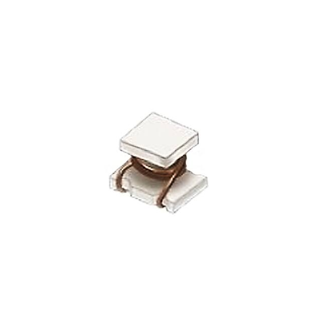
5. Appearance and Dimensions
Unit mass (typical value): 0.009 g
6. Marking
No marking.
MURATA MFG CO., LTD
�Spec No.: JELF243A_0052T-01
P3/10
7. Electrical Performance
No.
Item
7.1
Inductance
Specification
Meet chapter 3 ratings.
Test method
Measuring equipment: Keysight E4991A or the
equivalent
Measuring frequency:
Inductance
100 MHz 3.3 nH to 220 nH
Q
7.2
Q
Meet chapter 3 ratings.
10 MHz
270 nH to 470 nH
250 MHz
3.3 nH to 39 nH
200 MHz
47 nH to 68 nH
150 MHz
82 nH to 150 nH
100 MHz
180 nH to 220 nH
25.2 MHz 270 nH to 470 nH
Measuring method: see "Electrical performance:
Measuring method for inductance/Q" in the chapter
"14. Appendix".
7.3
DC resistance
Meet chapter 3 ratings.
Measuring equipment: digital multimeter
7.4
Self-resonant
frequency
Meet chapter 3 ratings.
Measuring equipment: Keysight N5230A or the
equivalent
7.5
Rated current
Product temperature rise: 20°C max.
Inductance change rate: within ±10%
Apply the rated current specified in chapter 3.
8. Mechanical Performance
No.
8.1
Item
Shear test
Specification
No significant mechanical damage or no
sign of electrode peeling off shall be
observed.
Test method
Test substrate: glass-epoxy substrate
Force application direction:
Applying force: 10 N
Holding time: 5 s±1 s
8.2
Bending test
No significant mechanical damage or no
sign of electrode peeling off shall be
observed.
Test substrate: glass-epoxy substrate (100 mm × 40
mm × 1.6 mm)
Pressurizing speed: 1 mm/s
Deflection: 2 mm
Holding time: 30 s
8.3
Vibration
Appearance shall have no significant
mechanical damage.
Oscillation frequency: 10 Hz to 55 Hz to 10 Hz, for
approx. 1 min
Total amplitude: 1.5 mm
Test time: 3 directions perpendicular to each other, 2 h
for each direction (6 h in total)
8.4
Solderability
90% or more of the outer electrode shall
be covered with new solder seamlessly.
Flux: immersed in ethanol solution with a rosin content
of 25(wt)% for 5 s to 10 s
Solder: Sn-3.0Ag-0.5Cu solder
Pre-heating: 150°C±10°C/60 s to 90 s
Solder temperature: 240°C±5°C
Immersion time: 3 s±1 s
MURATA MFG CO., LTD
�Spec No.: JELF243A_0052T-01
No.
8.5
P4/10
Item
Resistance to
soldering heat
Specification
Test method
Appearance: No significant mechanical
damage shall be observed.
Inductance change rate: within ±5%
Flux: immersed in ethanol solution with a rosin content
of 25(wt)% for 5 s to 10 s
Solder: Sn-3.0Ag-0.5Cu solder
Pre-heating: 150°C±10°C/60 s to 90 s
Solder temperature: 270°C±5°C
Immersion time: 10 s±1 s
Post-treatment: left at a room condition for 24 h±2 h
9. Environmental Performance
The product is soldered on a substrate for test.
No.
Item
Specification
Test method
9.1
Heat resistance
Appearance: No significant mechanical
damage shall be observed.
Inductance change rate: within ±5%
Q change rate: within ±20%
Temperature: 85°C±2°C
Test time: 1000 h (+48 h, -0 h)
Post-treatment: left at a room condition for 24 h±2 h
9.2
Cold resistance
Appearance: No significant mechanical
damage shall be observed.
Inductance change rate: within ±5%
Q change rate: within ±20%
Temperature: -40°C±2°C
Test time: 1000 h (+48 h, -0 h)
Post-treatment: left at a room condition for 24 h±2 h
9.3
Humidity
Appearance: No significant mechanical
damage shall be observed.
Inductance change rate: within ±5%
Q change rate: within ±20%
Temperature: 40°C±2°C
Humidity: 90% (RH) to 95% (RH)
Test time: 1000 h (+48 h, -0 h)
Post-treatment: left at a room condition for 24 h±2 h
9.4
Temperature cycle Appearance: No significant mechanical
damage shall be observed.
Inductance change rate: within ±5%
Q change rate: within ±20%
Single cycle conditions:
Step 1: -40°C±2°C/30 min±3 min
Step 2: ordinary temperature/10 min to 15 min
Step 3: +85°C±2°C/30 min±3 min
Step 4: ordinary temperature/10 min to 15 min
Number of testing: 10 cycles
Post-treatment: left at a room condition for 24 h±2 h
10. Specification of Packaging
10.1 Appearance and dimensions of tape (8 mm width/plastic tape)
A
1.75±0.2
B
2.3±0.2
t
2.0±0.1
t'
(0.3)
(in mm)
* The dimensions of the cavity are measured at its bottom.
MURATA MFG CO., LTD
�Spec No.: JELF243A_0052T-01
P5/10
10.2 Taping specifications
Packing quantity
(Standard quantity)
2000 pcs/reel
Packing method
The products are placed in embossed cavities of a plastic tape and sealed by a cover tape.
Feed hole position
The feed holes on the plastic tape are on the right side when the cover tape is pulled toward the user.
Joint
The plastic tape and the cover tape are seamless.
Number of missing
products
Number of missing products within 0.1% of the number per reel or 1 pc., whichever is greater, and are
not continuous. The specified quantity per reel is kept.
10.3 Break down force of tape
Break down force of cover tape
10 N min.
10.4 Peeling off force of cover tape
Speed of peeling off
300 mm/min
Peeling off force
165 to 180 degree
0.1 N to 0.7 N (The lower limit is for typical value.)
F
Cover tape
Plastic tape
10.5 Dimensions of leader section, trailer section and reel
A vacant section is provided in the leader (start) section and trailer (end) section of the tape for the product. The leader
section is further provided with an area consisting only of the cover tape. (See the diagram below.)
10.6 Marking for reel
Customer part number, Murata part number, inspection number (*1), RoHS marking (*2), quantity, etc.
*1 Expression of inspection No.: (1) Factory code
(2) Date
□□
○○○○
First digit: year/last digit of year
(1)
(2)
(3)
Second digit: month/Jan. to Sep.→1 to 9, Oct. to Dec.→O, N, D
Third, Fourth digit: day
(3) Serial No.
*2 Expression of RoHS marking: (1) RoHS regulation conformity
ROHSY
()
(2) Murata classification number
(1)
(2)
10.7 Marking on outer box (corrugated box)
Customer name, purchasing order number, customer part number, Murata part number, RoHS marking (*2), quantity, etc.
MURATA MFG CO., LTD
�Spec No.: JELF243A_0052T-01
P6/10
10.8 Specification of outer box
Label
H
D
W
11.
Dimensions of outer box
(mm)
W
D
H
186
186
93
Standard reel quantity
in outer box (reel)
5
* Above outer box size is typical. It depends on a
quantity of an order.
Caution
Restricted
applications
Please contact us before using our products for the applications listed below which require especially high
reliability for the prevention of defects which might directly cause damage to the third party's life, body or
property.
(1) Aircraft equipment
(2) Aerospace equipment
(3) Undersea equipment
(4) Power plant control equipment
(5) Medical equipment
(6) Transportation equipment (vehicles, trains, ships, etc.)
(7) Traffic signal equipment
(8) Disaster/crime prevention equipment
(9) Data-processing equipment
(10) Applications of similar complexity and/or reliability requirements
to the applications listed in the above
12. Precautions for Use
This product is designed to be mounted by soldering. If you want to use other mounting method, for example, using a
conductive adhesive, please consult us beforehand.
12.1 Land dimensions
The following diagram shows the recommended land dimensions for flow and reflow soldering.
The land dimensions are designed in consideration of electrical characteristics and mountability. Use of other land
dimensions may preclude achievement of performance. In some cases, it may result in poor solderability, including positional
shift. If you use other land pattern, consider it adequately.
a
0.8
b
3.0
c
1.2
(in mm)
12.2 Flux and solder used
Flux
• Use a rosin-based flux.
• Do not use a highly acidic flux with a halide content exceeding 0.2(wt)% (chlorine conversion value).
• Do not use a water-soluble flux.
Solder
• Use Sn-3.0Ag-0.5Cu solder.
• Standard thickness of solder paste: 200 μm to 300 μm
MURATA MFG CO., LTD
�Spec No.: JELF243A_0052T-01
P7/10
12.3 Soldering conditions (flow, reflow)
• Pre-heating should be in such a way that the temperature difference between solder and product surface is limited to 150°C
max.
Cooling into solvent after soldering also should be in such a way that the temperature difference is limited to 100°C max.
Insufficient pre-heating may cause cracks on the product, resulting in the deterioration of product quality.
• Standard soldering profile and the limit soldering profile is as follows.
The excessive limit soldering conditions may cause leaching of the electrode and/or resulting in the deterioration of product
quality.
(1) Flow
Temp.
(℃)
265℃±3℃
250℃
Limit Profile
150
Heating Time
60s min.
Standard Profile
Time. (s)
Standard profile
Limit profile
Pre-heating
150°C/60 s min.
150°C/60 s min.
Heating
250°C/4 s to 6 s
265°C±3°C/5 s
2 times
2 times
Number of flow cycles
(2) Reflow
Temp.
(℃)
260℃
245℃±3℃
230℃
220℃
Limit Profile
180
150
Standard Profile
30s~60s
60s max.
90s±30s
Time. (s)
Standard profile
Limit profile
Pre-heating
150°C to 180°C/90 s±30 s
150°C to 180°C/90 s±30 s
Heating
Above 220°C/30 s to 60 s
Above 230°C/60 s max.
245°C±3°C
260°C/10 s
2 times
2 times
Peak temperature
Number of reflow cycles
MURATA MFG CO., LTD
�Spec No.: JELF243A_0052T-01
P8/10
12.4 Reworking with soldering iron
The following requirements must be met to rework a soldered product using a soldering iron.
Item
Requirement
Pre-heating
150°C/approx. 1 min
Tip temperature of soldering iron
350°C max.
Power consumption of soldering iron
80 W max.
Tip diameter of soldering iron
Soldering time
ø3 mm max.
3 s (+1 s, -0 s)
Number of reworking operations
2 times max.
* Avoid a direct contact of the tip of the soldering iron with the product. Such a
direction contact may cause cracks in the ceramic body due to thermal shock.
12.5 Solder volume
Solder shall be used not to increase the volume too much.
An increased solder volume increases mechanical stress on the product. Exceeding solder volume may cause the failure of
mechanical or electrical performance.
12.6 Product's location
The following shall be considered when designing and laying out PCBs.
(1) PCB shall be designed so that products are not subject to mechanical stress due to warping the board.
[Products direction]
Products shall be located in the sideways direction (length: a < b) to the mechanical stress.
a
b
〈 Poor example〉
〈 Good example〉
(2) Components location on PCB separation
It is effective to implement the following measures, to reduce stress in separating the board.
It is best to implement all of the following three measures; however, implement as many measures as possible to reduce
stress.
Contents of measures
Stress level
(1) Turn the mounting direction of the component parallel to the
board separation surface.
A > D*1
(2) Add slits in the board separation part.
A>B
(3) Keep the mounting position of the component away from the
board separation surface.
A>C
*1 A > D is valid when stress is added vertically to the perforation as with hand separation.
If a cutting disc is used, stress will be diagonal to the PCB, therefore A > D is invalid.
MURATA MFG CO., LTD
�Spec No.: JELF243A_0052T-01
P9/10
(3) Mounting components near screw holes
When a component is mounted near a screw hole, it may be affected by the board deflection that occurs during the
tightening of the screw.
Mount the component in a position as far away from the screw holes as possible.
12.7 Handling of substrate
After mounting products on a substrate, do not apply any stress to the product caused by bending or twisting to the substrate
when cropping the substrate, inserting and removing a connector from the substrate or tightening screw to the substrate.
Excessive mechanical stress may cause cracking in the product.
Bending
Twisting
12.8 Cleaning
The product shall be cleaned under the following conditions.
(1) The cleaning temperature shall be 60°C max. If isopropyl alcohol (IPA) is used, the cleaning temperature shall be 40°C
max.
(2) Perform ultrasonic cleaning under the following conditions. Exercise caution to prevent resonance phenomenon in
mounted products and the PCB.
Item
Requirement
Power
Time
20 W/L max.
5 min max.
Frequency
28 kHz to 40 kHz
(3) Cleaner
Alcohol-based cleaner: IPA
Aqueous agent: PINE ALPHA ST-100S
(4) There shall be no residual flux or residual cleaner. When using aqueous agent, rinse the product with deionized water
adequately and completely dry it so that no cleaner is left.
* For other cleaning, consult our technical department.
12.9 Storage and transportation
Storage period
Use the product within 12 months after delivery.
If you do not use the product for more than 12 months, check solderability before using it.
Storage conditions
• The products shall be stored in a room not subject to rapid changes in temperature and humidity.
The recommended temperature range is -10°C to +40°C. The recommended relative humidity
range is 15% to 85%.
Keeping the product in corrosive gases, such as sulfur, chlorine gas or acid, oxidizes the
electrode, resulting in poor solderability or corrosion of the coil wire of the product.
• Do not keep products in bulk packaging. Doing so may cause collision between the products or
between the products and other products, resulting in core chipping or wire breakage.
• Do not place the products directly on the floor; they should be placed on a palette so that they are
not affected by humidity or dust.
• Avoid keeping the products in a place exposed to direct sunlight, heat or vibration.
Transportation
Excessive vibration and impact reduces the reliability of the products. Exercise caution when
handling the products.
MURATA MFG CO., LTD
�Spec No.: JELF243A_0052T-01
P10/10
12.10 Resin coating
The inductance value may change due to high cure-stress of resin to be used for coating/molding products.
A wire breakage issue may occur by mechanical stress caused by the resin, amount/cured shape of resin, or operating
condition etc. Some resin contains some impurities or chloride possible to generate chlorine by hydrolysis under some
operating condition may cause corrosion of wire of coil, leading to wire breakage.
So, please pay your careful attention when you select resin in case of coating/molding the products with the resin.
Prior to use the coating resin, please make sure no reliability issue is observed by evaluating products mounted on your
board.
12.11 Handling of product
• Sharp material such as a pair of tweezers or other material such as bristles of cleaning brush, shall not be touched to the
winding portion to prevent the breaking of wire.
• Mechanical shock should not be applied to the products mounted on the board to prevent the breaking of the core.
13.
Note
(1) Please make sure that your product has been evaluated in view of your specifications with our product being mounted to
your product.
(2) You are requested not to use our product deviating from the reference specifications.
(3) The contents of this reference specification are subject to change without advance notice. Please approve our product
specifications or transact the approval sheet for product specifications before ordering.
14. Appendix
Electrical performance: Measuring method for inductance/Q (Q measurement is applicable only when the Q value is included
in the rating table.)
Perform measurement using the method described below. (Perform correction for the error deriving from the measuring
terminal.)
(1) Residual elements and stray elements of the measuring terminal can be expressed by the F parameter for the 2-pole
terminal as shown in the figure below.
(2) The product's impedance value (Zx) and measured impedance value (Zm) can be expressed as shown below, by using
the respective current and voltage for input/output.
Zm=
V1
I1
Zx=
V2
I2
(3) Thus, the relationship between the product's impedance value (Zx) and measured impedance value (Zm) is as follows.
Zx=α
Zm-β
1-ZmΓ
Here,
α = D/A = 1
β = B/D = Zsm - (1 - Yom Zsm) Zss
Γ = C/A = Yom
Zsm: measured impedance of short chip
Zss: residual impedance of short chip (0.771 nH)
Yom: measured admittance when measuring terminal is open
(4) Calculate inductance Lx and Qx using the equations shown below.
Im (Zx)
Lx: inductance of chip coil
Lx=
2πf
Qx: Q of chip coil
Im (Zx)
Qx=
f: measuring frequency
Re (Zx)
MURATA MFG CO., LTD
�