OKDx-T/20-W12-xxx-C
www.murata-ps.com
20A Digital PoL DC-DC Converter Series
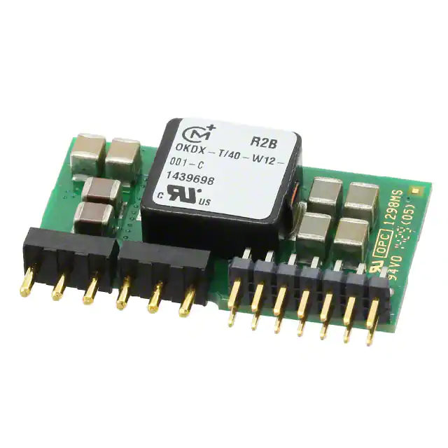
Typical units
FEATURES
PRODUCT OVERVIEW
Small package: 25.65 x 13.8 x 8.2 mm (1.01 x
0.543 x 0.323 in) SIP: 26.3 x 7.6 x 15.6 mm (1.035
x 0.30 x 0.614 in)
The OKDx-T/20-W12 series are high efficiency,
digital point-of-Load (PoL) DC-DC power converters
capable of delivering 20A/66W. Available in three
different package formats, through-hole, single-inline, and surface mount, these converters have a
typical efficiency of 97.1%. PMBus™ compatibility
allows monitoring and configuration of critical
system-level performance requirements. Apart from
0.6 V - 3.3 V output voltage range
High efficiency, typ. 97.1% at 5Vin, 3.3Vout half load
Configuration and Monitoring via PMBus™
Synchonization & phase spreading
Current sharing, Voltage Tracking & Voltage
margining
MTBF 20.2 Mh
Non-Linear Response for reduction of decoupling capacitor
Remote control & power good
Output short-circuit, output over voltage, & over
temperature protection
Certified to UL/IEC 60950-1
standard PoL performance and safety features like
OVP, OCP, OTP, and UVLO, these digital converters
have advanced features: digital current sharing (full
power, no derating), non-linear transient response,
optimized dead time control, synchronization, and
phase spreading. These converters are ideal for use
in telecommunications, networking, and distributed
power applications.
Power Management via PMBus™
Applications
Configurable soft-start/stop
Distributed power architectures
Configurable output voltage (Vout) and voltage
margins (Margin low and Margin high)
Intermediate bus voltage applications
Configurable protection limits for OVP, input over
voltage, input under voltage, over current, on/off,
and temperature
Network equipment
Servers and storage applications
Status monitor Vout, Iout, Vin, Temp, Power
good, and On/Off
PART NUMBER STRUCTURE
OKD x - T / 20 - W12 - xxx - C
Digital Non-isolated PoL
Y = Surface Mount
H = Horizontal Mount Through-Hole
X = SIP
Trimmable Output
Voltage Range
0.6 - 3.3Vdc
Maximum Rated Output
Current in Amps
RoHS Hazardous
Substance Compliance
C = RoHS-6 (does not claim EU RoHS exemption
7b – lead in solder)
Software Configuration Digits
(001 is positive turn-on logic)
(002 is negative turn-on logic)*
Input Voltage Range
4.5-14Vdc
*Special quantity order is required;
contact Murata Power Solutions for
MOQ and lead times.
PM
www.murata-ps.com/support
MDC_OKDx-T/20-W12-xxx-C.A05 Page 1 of 37
�OKDx-T/20-W12-xxx-C
20A Digital PoL DC-DC Converter Series
ORDERING GUIDE
Model Number
OKDY-T/20-W12-001-C
OKDH-T/20-W12-001-C
OKDX-T/20-W12-001-C
Output
0.6-3.3 V, 20 A/ 66 W
Absolute Maximum Ratings
Characteristics
TP1, TP2
Operating temperature (see Thermal Consideration section)
TS
Storage temperature
VI
Input voltage (See Operating Information Section for input and output voltage relations)
Logic I/O voltage
CTRL, SA0, SA1, SALERT, SCL, SDA, VSET, SYNC, GCB, PG
Ground voltage differential -S, PREF, GND
Analog pin voltage
VO, +S, VTRK
General and Safety
Safety
Calculated MTBF
Min
-40
-40
-0.3
-0.3
-0.3
-0.3
Conditions
Designed for UL/IEC/EN 60950 1
Telcordia SR-332, Issue 2 Method 1
Stress in excess of Absolute Maximum Ratings may cause permanent
damage. Absolute Maximum Ratings, sometimes referred to as no destruction
limits, are normally tested with one parameter at a time exceeding the limits
in the Electrical Specification. If exposed to stress above these limits, function
and performance may degrade in an unspecified manner.
Configuration File
This product is designed with a digital control circuit. The control circuit uses
a configuration file which determines the functionality and performance of the
product. The Electrical Specification table shows parameter values of func-
Min
Typ
Typ
20.2
Max
125
125
16
6.5
0.3
6.5
Max
Unit
°C
°C
V
V
V
V
Unit
Mhrs
tionality and performance with the default configuration file, unless otherwise
specified. The default configuration file is designed to fit most application
needs with focus on high efficiency. If different characteristics are required it
is possible to change the configuration file to optimize certain performance
characteristics. Note that current sharing operation requires changed configuration file.
In this Technical specification examples are included to show the possibilities with digital control. See Operating Information section for information
about trade offs when optimizing certain key performance characteristics.
VIN
VOUT
CI
CO
GND
+Sense
-Sense
(PGOOD)
(SA1)
SALERT
CTRL
VSET
Controller and digital interface
SYNC
SCL
SDA
SA0
GCB
VTRK
PREF
Fundamental Circuit Diagram
www.murata-ps.com/support
MDC_OKDx-T/20-W12-xxx-C.A05 Page 2 of 37
�OKDx-T/20-W12-xxx-C
20A Digital PoL DC-DC Converter Series
Electrical Specifications, OKDY-T/20-W12-xxx-C and OKDH-T/20-W12-xxx-C
TP1 = -30 to +95°C, VIN = 4.5 to 14 V, VIN > VOUT + 1.0 V
Typical values given at: TP1 = +25 °C, VIN = 12.0 V, max IOUT, unless otherwise specified under Conditions.
Default configuration file, 190 10-CDA 102 0206/001.
External CIN = 470 μF/10 mΩ, COUT = 470 μF/10 mΩ. See Operating Information section for selection of capacitor types.
Sense pins are connected to the output pins.
Characteristics
VI
Input voltage rise time
Conditions
monotonic
Output voltage without pin strap
Output voltage adjustment range
Output voltage adjustment including margining
Output voltage set-point resolution
VO
Load regulation; IO = 0 - 100%
VOac
Output ripple & noise
CO = 470 μF (minimum external capacitance). See Note 11
IO
Output current
IS
Static input current at max IO
Ilim
Current limit threshold
Isc
Unit
V/ms
3.3
3.63
V
V
V
% Vo
See Note 17
-1
1
%
-2
2
%
0.60
0.54
±0.025
Short circuit current
4.7
2
2
2
3
3
2
2
2
20
30
40
60
VO = 0.6 V
VO = 1.0 V
VO = 1.8 V
VO = 3.3 V
VO = 0.6 V
VO = 1.0 V
VO = 1.8 V
VO = 3.3 V
VO = 0.6 V
VO = 1.0 V
VO = 1.8 V
VO = 3.3 V
See Note 18
VO = 0.6 V
VO = 1.0 V
VO = 1.8 V
VO = 3.3 V
0.001
RMS, hiccup mode, See Note 3
Efficiency
max IO
Pd
Power dissipation at max IO
Pli
Input idling power
(no load)
Default configuration: Continues
Conduction Mode, CCM
PCTRL
Input standby power
Turned off with
CTRL-pin
Ci
Internal input capacitance
Ω
mV
mV
mVp-p
20
1.26
1.94
3.31
5.89
22
50% of max IO
Max
2.4
Internal resistance +S/-S to VOUT/GND
Line regulation
Typ
1.2
Including line, load, temp.
See Note 14
Current sharing operation
See Note 15
Output voltage accuracy
Min
A
30
VO = 0.6 V
VO = 1.0 V
VO = 1.8 V
VO = 3.3 V
8
6
5
4
VO = 0.6 V
VO = 1.0 V
VO = 1.8 V
VO = 3.3 V
VO = 0.6 V
VO = 1.0 V
VO = 1.8 V
VO = 3.3 V
VO = 0.6 V
VO = 1.0 V
VO = 1.8 V
VO = 3.3 V
VO = 0.6 V
VO = 1.0 V
VO = 1.8 V
VO = 3.3 V
84.0
89.3
92.8
94.8
79.3
86.0
90.7
93.6
3.12
3.25
3.68
4.52
0.56
0.57
0.68
0.99
Default configuration:
Monitoring enabled,
Precise timing enabled
180
70
A
A
A
%
%
W
W
mW
μF
www.murata-ps.com/support
MDC_OKDx-T/20-W12-xxx-C.A05 Page 3 of 37
�OKDx-T/20-W12-xxx-C
20A Digital PoL DC-DC Converter Series
Characteristics
Co
Internal output capacitance
Total external output capacitance
COUT
ESR range of capacitors
(per single capacitor)
Vtr1
ttr1
fs
Load transient peak
voltage deviation
(H to L)
Load step 25-75-25%
of max IO
Default configuration
di/dt = 2 A/μs
CO = 470 μF (minimum external
capacitance) see Note 12
Load transient recovery
time, Note 5
(H to L)
Load step 25-75-25%
of max IO
Default configuration
di/dt = 2 A/μs
CO = 470 μF (minimum external
capacitance) see Note 12
Switching frequency
Switching frequency range
Switching frequency set-point accuracy
Control Circuit PWM Duty Cycle
Minimum Sync Pulse Width
Input Clock Frequency Drift Tolerance
Input Under Voltage Lockout,
UVLO
Input Over Voltage Protection,
IOVP
Power Good, PG,
See Note 2
Output voltage
Over/Under Voltage Protection,
OVP/UVP
Over Current Protection,
OCP
Over Temperature Protection,
OTP at P1
See Note 8
UVLO threshold
UVLO threshold range
Set point accuracy
UVLO hysteresis
UVLO hysteresis range
Delay
Fault response
IOVP threshold
IOVP threshold range
Set point accuracy
IOVP hysteresis
IOVP hysteresis range
Delay
Fault response
PG threshold
PG hysteresis
PG delay
PG delay range
UVP threshold
UVP threshold range
UVP hysteresis
OVP threshold
OVP threshold range
UVP/OVP response time
UVP/OVP
response time range
Fault response
OCP threshold
OCP threshold range
Protection delay,
Protection delay range
Fault response
OTP threshold
OTP threshold range
OTP hysteresis
OTP hysteresis range
Fault response
Conditions
Min
Typ
200
See Note 9
300
15 000
Unit
μF
μF
See Note 9
5
30
mΩ
VO = 0.6 V
85
VO = 1.0 V
85
VO = 1.8 V
90
VO = 3.3 V
135
VO = 0.6 V
80
VO = 1.0 V
90
VO = 1.8 V
100
VO = 3.3 V
100
mV
μs
320
200-640
PMBus™ configurable
External clock source
Max
-5
5
150
-13
5
95
13
3.85
3.85-14
PMBus™ configurable
-150
150
0.35
0-10.15
PMBus™ configurable
2.5
See Note 3
Automatic restart, 70 ms
16
4.2-16
PMBus™ configurable
-150
PMBus™ configurable
150
1
0-11.8
2.5
See Note 3
PMBus™ configurable
PMBus™ configurable
PMBus™ configurable
PMBus™ configurable
See Note 3
PMBus™ configurable
See Note 4
PMBus™ configurable
See Note 3
PMBus™ configurable
PMBus™ configurable
See Note 3
kHz
kHz
%
%
ns
%
V
V
mV
V
V
μs
V
V
mV
V
V
μs
Automatic restart, 70 ms
90
5
10
0-500
85
0-100
5
115
100-115
25
% VO
% VO
ms
s
% VO
% VO
% VO
% VO
% VO
μs
5-60
μs
Automatic restart, 70 ms
26
0-26
32
1-32
Automatic restart, 70 ms
120
-40…+120
15
0-160
Automatic restart, 240 ms
A
A
Tsw
Tsw
C
C
C
C
www.murata-ps.com/support
MDC_OKDx-T/20-W12-xxx-C.A05 Page 4 of 37
�OKDx-T/20-W12-xxx-C
20A Digital PoL DC-DC Converter Series
Characteristics
VIL
Logic input low threshold
VIH
Logic input high threshold
IIL
Logic input low sink current
VOL
Logic output low signal level
VOH
Logic output high signal level
Logic output low sink current
IOL
Logic output high source current
IOH
Setup time, SMBus
tset
thold
Hold time, SMBus
tfree
Bus free time, SMBus
Cp
Internal capacitance on logic pins
Conditions
SYNC, SA0, SA1, SCL, SDA, GCB, CTRL,
VSET
CTRL
Initialization time
See Note 10
See Note 16
PMBus™ configurable
Default configuration:
CTRL controlled
Precise timing enabled
PMBus™ controlled
Precise timing disabled
Current sharing operation
Delay duration
Delay duration range
Output Voltage
Delay Time
See Note 6
Output Voltage
Ramp Time
See Note 13
Delay accuracy
turn-on
Delay accuracy
turn-off
Ramp duration
Ramp duration range
Ramp time accuracy
VTRK Input Bias Current
VTRK Tracking Ramp Accuracy (VO - VVTRK)
VTRK Regulation Accuracy (VO - VVTRK)
Current difference between products in a current sharing group
SYNC, SCL, SDA, SALERT, GCB, PG
See Note 1
See Note 1
See Note 1
READ_IOUT vs IO
Max
0.8
2
0.6
0.4
2.25
4
2
10
Current sharing operation
VVTRK = 5.5 V
100% tracking, see Note 7
Current sharing operation
2 phases, 100% tracking
VO = 1.0 V, 10 ms ramp
100% Tracking
Current sharing operation
100% Tracking
Steady state operation
Ramp-up
IO =0-20 A, TP1 = 0 to +95 °C
VI = 4.5-14 V, VO = 1.0 V
IO =0-20 A, TP1 = 0 to +95 °C
VI = 4.5-14 V, VO = 0.6-3.3 V
Note 1: See section I2C/SMBus Setup and Hold Times – Definitions.
Note 2: Monitorable over PMBus™ Interface.
Note 3: Automatic restart ~70 or 240 ms after fault if the fault is no longer present. Continuous restart attempts if the
fault reappear after restart. See Operating Information and AN302 for other fault response options.
Note 4: Tsw is the switching period.
Note 5: Within ±3% of VO
Note 6: See section Soft-start Power Up.
Note 7: Tracking functionality is designed to follow a VTRK signal with slew rate < 2.4 V/ms. For faster VTRK signals
accuracy will depend on the regulator bandwidth.
Note 8: See section Over Temperature Protection (OTP).
Note 9: See section External Capacitors.
Unit
V
V
mA
V
V
mA
mA
ns
ns
ms
pF
35
10
2-500000
ms
±0.25
ms
-0.25/+4
ms
-0.25/+4
ms
ms
10
0-200
100
20
PMBus™ configurable
READ_VIN vs VI
READ_VOUT vs VO
READ_IOUT vs IO
Typ
300
250
2
Number of products in a current sharing group
Monitoring accuracy
Min
110
-100
ms
μs
%
200
100
±100
μA
mV
mV
-1
1
%
-2
2
%
Max 2 x READ_IOUT monitoring accuracy
2
7
A
3
1
%
%
±1.4
A
±2.6
A
Note 10: See section Initialization Procedure.
Note 11: See graph Output Ripple vs External Capacitance and Operating information section Output Ripple and Noise.
Note 12: See graph Load Transient vs. External Capacitance and Operating information section External Capacitors.
Note 13: Time for reaching 100% of nominal Vout.
Note 14: For Vout < 1.0 V accuracy is ±10 mV. For further deviations see section Output Voltage Adjust using PMBus™.
Note 15: Accuracy here means deviation from ideal output voltage level given by configured droop and actual load.
Includes line, load and temperature variations.
Note 16: For current sharing the Output Voltage Delay Time must be reconfigured to minimum 15 ms.
Note 17: For steady state operation above 1.05 x 3.3 V, please contact your local Murata sales representative.
Note 18: A minimum load current is not required if Low Power mode is used (monitoring disabled).
www.murata-ps.com/support
MDC_OKDx-T/20-W12-xxx-C.A05 Page 5 of 37
�OKDx-T/20-W12-xxx-C
20A Digital PoL DC-DC Converter Series
Typical Characteristics
Efficiency and Power Dissipation
Efficiency vs. Output Current, VI = 5 V
Power Dissipation vs. Output Current, VI = 5 V
[%]
100
[W]
5
4
95
3
90
85
0,6 V
1,0 V
2
80
1,8 V
3,3 V
1
0,6 V
1,0 V
1,8 V
3,3 V
75
0
0
4
8
12
16
20 [A]
0
4
8
12
16
20 [A]
Efficiency vs. load current and output voltage:
TP1 = +25 °C, VI = 5 V, fsw = 320 kHz, CO = 470 μF/10 m.
Dissipated power vs. load current and output voltage:
TP1 = +25 °C, VI = 5 V, fsw = 320 kHz, CO = 470 μF/10 m.
Efficiency vs. Output Current, VI = 12 V
Power Dissipation vs. Output Current, VI = 12 V
[W]
5
[%]
100
4
95
90
3
0,6 V
85
1,0 V
1,8 V
80
3,3 V
75
0,6 V
2
1,0 V
1,8 V
1
3,3 V
0
0
4
8
12
16
20 [A]
0
4
8
12
16
20 [A]
Efficiency vs. load current and output voltage at
TP1 = +25 °C, VI = 12 V, fsw = 320 kHz, CO = 470 μF/10 m.
Dissipated power vs. load current and output voltage:
TP1 = +25 °C, VI = 12 V, fsw = 320 kHz, CO = 470 μF/10 m.
Efficiency vs. Output Current and
Switching Frequency
Power Dissipation vs. Output Current and
Switching frequency
[%]
95
[W]
5
90
200
kHz
4
200
kHz
85
320
kHz
3
320
kHz
80
480
kHz
2
480
kHz
75
640
kHz
1
640
kHz
0
70
0
4
8
12
16
Efficiency vs. load current and switch frequency at
TP1 = +25 °C, VI = 12 V, VO = 1.0 V, CO = 470 μF/10 m
Default configuration except changed frequency
20 [A]
0
4
8
12
16
20 [A]
Dissipated power vs. load current and switch frequency at
TP1 = +25 °C, VI = 12 V, VO = 1.0 V, CO = 470 μF/10 m
Default configuration except changed frequency
www.murata-ps.com/support
MDC_OKDx-T/20-W12-xxx-C.A05 Page 6 of 37
�OKDx-T/20-W12-xxx-C
20A Digital PoL DC-DC Converter Series
Typical Characteristics
Load Transient
Load Transient vs. External Capacitance, VO = 1.0 V
Load Transient vs. External Capacitance, VO = 3.3 V
[mV]
200
[mV]
200
160
Default
PID/NLR
120
Opt. PID,
No NLR
80
Default PID,
Opt. NLR
40
Opt.
PID/NLR
Default
PID/NLR
150
Opt. PID,
No NLR
100
Default PID,
Opt. NLR
50
Opt.
PID/NLR
0
0
0
1
2
3
4
0
5 [mF]
1
2
3
4
5 [mF]
Load transient peak voltage deviation vs. external capacitance.
Step-change (5-15-5 A). Parallel coupling of capacitors with 470 μF/10 Pȍ,
TP1 = +25 °C, VI = 12 V, VO = 1.0 V, fsw = 320 kHz, di/dt = 2 A/μs
Load transient peak voltage deviation vs. external capacitance.
Step-change (5-15-5 A). Parallel coupling of capacitors with 470 μF/10 Pȍ,
TP1 = +25 °C, VI = 12 V, VO = 3.3 V, fsw = 320 kHz, di/dt = 2 A/μs
Load transient vs. Switch Frequency
Output Load Transient Response, Default PID/NLR
[mV]
240
200
Default
PID/NLR
160
Opt. PID, No
NLR
120
Default PID,
Opt. NLR
80
Opt.
PID/NLR
40
0
200
300
400
500
600 [kHz]
Load transient peak voltage deviation vs. frequency.
Step-change (5-15-5 A).
TP1 = +25 °C, VI = 12 V, VO = 1.0 V, CO = 470 μF/10 m
Output voltage response to load current
step-change (5-15-5 A) at:
TP1 = +25 °C, VI = 12 V, VO = 1.0 V
di/dt = 2 A/μs, fsw = 320 kHz,
CO = 470 μF/10 m
Top trace: output voltage (200
mV/div.).
Bottom trace: load current (5
A/div.).
Time scale: (0.1 ms/div.).
www.murata-ps.com/support
MDC_OKDx-T/20-W12-xxx-C.A05 Page 7 of 37
�OKDx-T/20-W12-xxx-C
20A Digital PoL DC-DC Converter Series
Typical Characteristics
Output Current Characteristic
Output Current Derating, VO = 0.6 V
Output Current Derating, VO = 1.0 V
[A]
25
[A]
25
3.0 m/s
3.0 m/s
20
2.0 m/s
20
2.0 m/s
15
1.0 m/s
15
1.0 m/s
10
0.5 m/s
10
0.5 m/s
Nat. Conv.
5
0
Nat. C onv.
5
0
60
70
80
90
100
110
60
120 [°C]
70
80
90
100
110
120 [°C]
Available load current vs. ambient air temperature and airflow at
VO = 0.6 V, VI = 12 V. See Thermal Consideration section.
Available load current vs. ambient air temperature and airflow at
VO = 1.0 V, VI = 12 V. See Thermal Consideration section.
Output Current Derating, VO = 1.8 V
Output Current Derating, VO = 3.3 V
[A]
25
[A]
25
3.0 m/s
3.0 m/s
20
2.0 m/s
20
2.0 m/s
15
1.0 m/s
15
1.0 m/s
10
0.5 m/s
10
0.5 m/s
Nat. C onv.
5
Nat. Conv.
5
0
0
60
70
80
90
100
110
60
120 [°C]
Available load current vs. ambient air temperature and airflow at
VO = 1.8 V, VI = 12 V. See Thermal Consideration section.
70
80
90
100
110
120 [°C]
Available load current vs. ambient air temperature and airflow at
VO = 3.3 V, VI = 12 V. See Thermal Consideration section.
Current Limit Characteristics, VO = 1.0 V
Current Limit Characteristics, VO = 3.3 V
[V]
[V]
1,2
4,0
1,0
3,0
0,8
4.5 V
5.0 V
0,6
12 V
0,4
4.5 V
5.0 V
2,0
12 V
14 V
14 V
1,0
0,2
0,0
0,0
20
22
24
26
28
30 [A]
20
22
24
26
28
30 [A]
Output voltage vs. load current at TP1 = +25 °C, VO = 1.0 V.
Output voltage vs. load current at TP1 = +25 °C, VO = 3.3 V.
Note: Output enters hiccup mode at current limit.
Output enters hiccup mode at current limit.
www.murata-ps.com/support
MDC_OKDx-T/20-W12-xxx-C.A05 Page 8 of 37
�OKDx-T/20-W12-xxx-C
20A Digital PoL DC-DC Converter Series
Typical Characteristics
Output Voltage
Output Ripple & Noise, VO = 1.0 V
Output Ripple & Noise, VO = 3.3 V
Output voltage ripple at: TP1 = +25 °C, Trace: output voltage (20 mV/div.).
VI = 12 V, CO =4 70 μF/10 m
Time scale: (2 μs/div.).
IO = 20 A
Output voltage ripple at: TP1 = +25 °C, Trace: output voltage (20 mV/div.).
VI = 12 V, CO = 470 μF/10 m
Time scale: (2 μs/div.).
IO = 20 A
Output Ripple vs. Input Voltage
Output Ripple vs. Frequency
[mVpk-pk]
70
[mVpk-pk]
80
60
70
60
50
0.6 V
40
1.0 V
30
1.8 V
20
3.3 V
10
0.6 V
50
1.0 V
40
1.8 V
30
3.3 V
20
10
0
5
7
9
11
0
200
[V]
13
300
400
500
600 [kHz]
Output voltage ripple Vpk-pk at: TP1 = +25 °C, CO = 470 μF/10 m, IO = 20 A
Output voltage ripple Vpk-pk at: TP1 = +25 °C, VI = 12 V, CO = 470 μF/10 m,
IO = 20 A. Default configuration except changed frequency.
Output Ripple vs. External Capacitance
Load regulation, VO = 1.0 V
[mV]
60
[V]
1,010
50
0.6V
40
1.0 V
30
1.8 V
20
3.3 V
10
0
1,005
4.5 V
5.0 V
1,000
12 V
14 V
0,995
0,990
0
1
2
3
4
5 [mF]
Output voltage ripple Vpk-pk at: TP1 = +25 °C, VI = 12 V, IO = 20 A.
Parallel coupling of capacitors with 470 μF/10 mȍ,
0
4
8
12
16
20 [A]
Load regulation at Vo = 1.0 V, TP1 = +25 °C, CO = 470 μF/10 m
www.murata-ps.com/support
MDC_OKDx-T/20-W12-xxx-C.A05 Page 9 of 37
�OKDx-T/20-W12-xxx-C
20A Digital PoL DC-DC Converter Series
Typical Characteristics
Start-up and shut-down
Start-up by input source
Start-up enabled by connecting VI at:
TP1 = +25 °C, VI = 12 V, VO = 1.0 V
CO = 470 μF/10 m, IO = 20 A
Shut-down by input source
Top trace: output voltage (0.5 V/div.).
Bottom trace: input voltage (5 V/div.).
Time scale: (20 ms/div.).
Start-up by CTRL signal
Start-up by enabling CTRL signal at:
TP1 = +25 °C, VI = 12 V, VO = 1.0 V
CO = 470 μF/10 m, IO = 20 A
Shut-down enabled by disconnecting
VI at:
TP1 = +25 °C, VI = 12 V, VO = 1.0 V
CO = 470 μF/10 m, IO = 20 A
Top trace: output voltage (0.5 V/div.).
Bottom trace: input voltage (5 V/div.).
Time scale: (2 ms/div.).
Shut-down by CTRL signal
Top trace: output voltage (0.5 V/div.).
Bottom trace: CTRL signal (5 V/div.).
Time scale: (20 ms/div.).
Shut-down enabled by disconnecting
VI at:
TP1 = +25 °C, VI = 12 V, VO = 1.0 V
CO = 470 μF/10 m, IO = 20 A
Top trace: output voltage (0.5 V/div).
Bottom trace: CTRL signal (5 V/div.).
Time scale: (2 ms/div.).
www.murata-ps.com/support
MDC_OKDx-T/20-W12-xxx-C.A05 Page 10 of 37
�OKDx-T/20-W12-xxx-C
20A Digital PoL DC-DC Converter Series
Electrical Specifications, OKDX-T/20-W12-xxx-C
TP1 = -30 to +95 °C, VI = 4.5 to 14 V, VI > VO + 1.0 V
Typical values given at: TP1 = +25 °C, VI = 12.0 V, max IO, unless otherwise specified under Conditions.
Default configuration file, 190 10-CDA 102 0259/001.
External CIN = 470 μF/10 mΩ, COUT = 470 μF/10 mΩ. See Operating Information section for selection of capacitor types.
Sense pins are connected to the output pins.
Characteristics
VI
Input voltage rise time
Conditions
monotonic
Output voltage without pin strap
Output voltage adjustment range
Output voltage adjustment including margining
Output voltage set-point resolution
VO
Load regulation; IO = 0 - 100%
VOac
Output ripple & noise
CO = 470 μF (minimum external capacitance). See Note 11
IO
Output current
IS
Static input current at max IO
Ilim
Current limit threshold
Isc
Short circuit current
RMS, hiccup mode, See Note 3
Efficiency
max IO
Pd
Power dissipation at max IO
Pli
Input idling power
(no load)
Default configuration: Continues
Conduction Mode, CCM
PCTRL
Input standby power
Turned off with
CTRL-pin
Ci
Co
Internal input capacitance
Internal output capacitance
Max
2.4
Unit
V/ms
3.3
3.63
V
V
V
% Vo
1
%
2
%
±0.025
-1
-2
4.7
2
2
3
3
3
2
2
2
20
30
40
60
VO = 0.6 V
VO = 1.0 V
VO = 1.8 V
VO = 3.3 V
VO = 0.6 V
VO = 1.0 V
VO = 1.8 V
VO = 3.3 V
VO = 0.6 V
VO = 1.0 V
VO = 1.8 V
VO = 3.3 V
See Note 18
VO = 0.6 V
VO = 1.0 V
VO = 1.8 V
VO = 3.3 V
0.001
Ω
mV
mV
mVp-p
20
1.29
1.97
3.34
5.92
22
50% of max IO
�
See Note 17
0.60
0.54
Internal resistance +S/-S to VOUT/GND
Line regulation
Typ
1.2
Including line, load, temp.
See Note 14
Current sharing operation
See Note 15
Output voltage accuracy
Min
A
30
VO = 0.6 V
VO = 1.0 V
VO = 1.8 V
VO = 3.3 V
8
6
5
4
VO = 0.6 V
VO = 1.0 V
VO = 1.8 V
VO = 3.3 V
VO = 0.6 V
VO = 1.0 V
VO = 1.8 V
VO = 3.3 V
VO = 0.6 V
VO = 1.0 V
VO = 1.8 V
VO = 3.3 V
VO = 0.6 V
VO = 1.0 V
VO = 1.8 V
VO = 3.3 V
83.5
89.0
92.7
94.8
78.0
85.3
90.4
93.5
3.40
3.45
3.86
4.62
0.56
0.57
0.69
1.00
Default configuration:
Monitoring enabled,
Precise timing enabled
180
70
200
A
A
A
%
%
W
W
mW
μF
μF
www.murata-ps.com/support
MDC_OKDx-T/20-W12-xxx-C.A05 Page 11 of 37
�OKDx-T/20-W12-xxx-C
20A Digital PoL DC-DC Converter Series
Characteristics
Total external output capacitance
COUT
ESR range of capacitors
(per single capacitor)
Vtr1
ttr1
fs
Load transient peak
voltage deviation
(H to L)
Load step 25-75-25%
of max IO
Default configuration
di/dt = 2 A/μs
CO = 470 μF (minimum external
capacitance) see Note 12
Load transient recovery
time, Note 5
(H to L)
Load step 25-75-25%
of max IO
Default configuration
di/dt = 2 A/μs
CO = 470 μF (minimum external
capacitance) see Note 12
Switching frequency
Switching frequency range
Switching frequency set-point accuracy
Control Circuit PWM Duty Cycle
Minimum Sync Pulse Width
Input Clock Frequency Drift Tolerance
Input Under Voltage Lockout,
UVLO
Input Over Voltage Protection,
IOVP
Power Good, PG,
See Note 2
Output voltage
Over/Under Voltage Protection,
OVP/UVP
Over Current Protection,
OCP
Over Temperature Protection,
OTP at P1
See Note 8
UVLO threshold
UVLO threshold range
Set point accuracy
UVLO hysteresis
UVLO hysteresis range
Delay
Fault response
IOVP threshold
IOVP threshold range
Set point accuracy
IOVP hysteresis
IOVP hysteresis range
Delay
Fault response
PG threshold
PG hysteresis
PG delay
PG delay range
UVP threshold
UVP threshold range
UVP hysteresis
OVP threshold
OVP threshold range
UVP/OVP response time
UVP/OVP
response time range
Fault response
OCP threshold
OCP threshold range
Protection delay,
Protection delay range
Fault response
OTP threshold
OTP threshold range
OTP hysteresis
OTP hysteresis range
Fault response
Conditions
See Note 9
Min
300
See Note 9
5
Typ
VO = 0.6 V
75
VO = 1.0 V
80
VO = 1.8 V
105
VO = 3.3 V
120
VO = 0.6 V
40
VO = 1.0 V
50
VO = 1.8 V
100
VO = 3.3 V
100
Unit
μF
30
mΩ
mV
μs
320
200-640
PMBus™ configurable
External clock source
Max
15 000
-5
5
150
-13
5
95
13
3.85
3.85-14
PMBus™ configurable
-150
150
0.35
0-10.15
PMBus™ configurable
2.5
See Note 3
Automatic restart, 70 ms
16
4.2-16
PMBus™ configurable
-150
PMBus™ configurable
150
1
0-11.8
2.5
See Note 3
PMBus™ configurable
PMBus™ configurable
PMBus™ configurable
PMBus™ configurable
See Note 3
PMBus™ configurable
See Note 4
PMBus™ configurable
See Note 3
PMBus™ configurable
PMBus™ configurable
See Note 3
kHz
kHz
%
%
ns
%
V
V
mV
V
V
μs
V
V
mV
V
V
μs
Automatic restart, 70 ms
90
5
10
0-500
85
0-100
5
115
100-115
25
% VO
% VO
ms
s
% VO
% VO
% VO
% VO
% VO
μs
5-60
μs
Automatic restart, 70 ms
26
0-26
5
1-32
Automatic restart, 70 ms
120
-40…+120
15
0-160
Automatic restart, 240 ms
A
A
Tsw
Tsw
C
C
C
C
www.murata-ps.com/support
MDC_OKDx-T/20-W12-xxx-C.A05 Page 12 of 37
�OKDx-T/20-W12-xxx-C
20A Digital PoL DC-DC Converter Series
Characteristics
VIL
Logic input low threshold
VIH
Logic input high threshold
IIL
Logic input low sink current
VOL
Logic output low signal level
VOH
Logic output high signal level
Logic output low sink current
IOL
Logic output high source current
IOH
tset
Setup time, SMBus
Hold time, SMBus
thold
tfree
Bus free time, SMBus
Internal capacitance on logic pins
Cp
Conditions
SYNC, SA0, SA1, SCL, SDA, GCB, CTRL,
VSET
CTRL
Initialization time
See Note 10
See Note 16
PMBus™ configurable
Default configuration:
CTRL controlled
Precise timing enabled
PMBus™ controlled
Precise timing disabled
Current sharing operation
Delay duration
Delay duration range
Output Voltage
Delay Time
See Note 6
Output Voltage
Ramp Time
See Note 13
Delay accuracy
turn-on
Delay accuracy
turn-off
Ramp duration
Ramp duration range
Ramp time accuracy
VTRK Input Bias Current
VTRK Tracking Ramp Accuracy (VO - VVTRK)
VTRK Regulation Accuracy (VO - VVTRK)
Current difference between products in a current sharing group
SYNC, SCL, SDA, SALERT, GCB, PG
See Note 1
See Note 1
See Note 1
READ_IOUT vs IO
Max
0.8
2
0.6
0.4
2.25
4
2
10
Current sharing operation
VVTRK = 5.5 V
100% tracking, see Note 7
Current sharing operation
2 phases, 100% tracking
VO = 1.0 V, 10 ms ramp
100% Tracking
Current sharing operation
100% Tracking
Steady state operation
Ramp-up
IO =0-20 A, TP1 = 0 to +95 °C
VI = 4.5-14 V, VO = 1.0 V
IO =0-20 A, TP1 = 0 to +95 °C
VI = 4.5-14 V, VO = 0.6-3.3 V
Note 1: See section I2C/SMBus Setup and Hold Times – Definitions.
Note 2: Monitorable over PMBus™ Interface.
Note 3: Automatic restart ~70 or 240 ms after fault if the fault is no longer present. Continuous restart attempts if the
fault reappear after restart. See Operating Information and AN302 for other fault response options.
Note 4: Tsw is the switching period.
Note 5: Within ±3% of VO
Note 6: See section Soft-start Power Up.
Note 7: Tracking functionality is designed to follow a VTRK signal with slew rate < 2.4 V/ms. For faster VTRK signals
accuracy will depend on the regulator bandwidth.
Note 8: See section Over Temperature Protection (OTP).
Note 9: See section External Capacitors.
Unit
V
V
mA
V
V
mA
mA
ns
ns
ms
pF
35
10
2-500000
ms
±0.25
ms
-0.25/+4
ms
-0.25/+4
ms
ms
10
0-200
100
20
PMBus™ configurable
READ_VIN vs VI
READ_VOUT vs VO
READ_IOUT vs IO
Typ
300
250
2
Number of products in a current sharing group
Monitoring accuracy
Min
110
-100
ms
μs
%
200
100
±100
μA
mV
mV
-1
1
%
-2
2
%
Max 2 x READ_IOUT monitoring accuracy
2
7
A
3
1
%
%
±1.4
A
±2.6
A
Note 10: See section Initialization Procedure.
Note 11: See graph Output Ripple vs External Capacitance and Operating information section Output Ripple and Noise.
Note 12: See graph Load Transient vs. External Capacitance and Operating information section External Capacitors.
Note 13: Time for reaching 100% of nominal Vout.
Note 14: For Vout < 1.0 V accuracy is ±10 mV. For further deviations see section Output Voltage Adjust using PMBus™.
Note 15: Accuracy here means deviation from ideal output voltage level given by configured droop and actual load.
Includes line, load and temperature variations.
Note 16: For current sharing the Output Voltage Delay Time must be reconfigured to minimum 15 ms.
Note 17: For steady state operation above 1.05 x 3.3 V, please contact your local Murata sales representative.
Note 18: A minimum load current is not required if Low Power mode is used (monitoring disabled).
www.murata-ps.com/support
MDC_OKDx-T/20-W12-xxx-C.A05 Page 13 of 37
�OKDx-T/20-W12-xxx-C
20A Digital PoL DC-DC Converter Series
Typical Characteristics
Efficiency and Power Dissipation
Efficiency vs. Output Current, VI = 5 V
Power Dissipation vs. Output Current, VI = 5 V
[%]
100
[W]
5
95
4
90
3
0,6 V
85
1,0 V
1,8 V
3,3 V
80
75
0,6 V
2
1,0 V
1,8 V
1
3,3 V
0
0
4
8
12
16
20 [A]
0
4
8
12
16
20 [A]
Efficiency vs. load current and output voltage:
TP1 = +25 °C, VI = 5 V, fsw = 320 kHz, CO = 470 μF/10 m.
Dissipated power vs. load current and output voltage:
TP1 = +25 °C, VI = 5 V, fsw = 320 kHz, CO = 470 μF/10 m.
Efficiency vs. Output Current, VI = 12 V
Power Dissipation vs. Output Current, VI = 12 V
[W]
5
[%]
100
4
95
3
90
0,6 V
1,0 V
85
1,8 V
80
3,3 V
75
0,6 V
2
1,0 V
1,8 V
1
3,3 V
0
0
4
8
12
16
0
20 [A]
4
8
12
16
20 [A]
Efficiency vs. load current and output voltage at
TP1 = +25 °C, VI = 12 V, fsw = 320 kHz, CO = 470 μF/10 m.
Dissipated power vs. load current and output voltage:
TP1 = +25 °C, VI=12 V, fsw = 320 kHz, CO = 470 μF/10 m.
Efficiency vs. Output Current and
Switching Frequency
Power Dissipation vs. Output Current and
Switching frequency
[%]
95
[W]
5
90
200
kHz
4
200
kHz
85
320
kHz
3
320
kHz
80
480
kHz
2
480
kHz
75
640
kHz
1
640
kHz
70
0
0
4
8
12
16
Efficiency vs. load current and switch frequency at
TP1 = +25 °C, VI = 12 V, VO = 1.0 V, CO = 470 μF/10 m
Default configuration except changed frequency
20 [A]
0
4
8
12
16
20 [A]
Dissipated power vs. load current and switch frequency at
TP1 = +25 °C, VI = 12 V, VO = 1.0 V, CO = 470 μF/10 m
Default configuration except changed frequency
www.murata-ps.com/support
MDC_OKDx-T/20-W12-xxx-C.A05 Page 14 of 37
�OKDx-T/20-W12-xxx-C
20A Digital PoL DC-DC Converter Series
Typical Characteristics
Load Transient
Load Transient vs. External Capacitance, VO = 1.0 V
Load Transient vs. External Capacitance, VO = 3.3 V
[mV]
160
[mV]
160
Default
PID/NLR
120
Opt. PID,
No NLR
80
Default PID,
Opt. NLR
40
Opt.
PID/NLR
Default
PID/NLR
120
Opt. PID,
No NLR
80
Default PID,
Opt. NLR
40
Opt.
PID/NLR
0
0
0
1
2
3
4
0
5 [mF]
1
2
3
4
5 [mF]
Load transient peak voltage deviation vs. external capacitance.
Step-change (5-15-5 A). Parallel coupling of capacitors with 470 μF/10 Pȍ,
TP1 = +25 °C, VI = 12 V, VO = 1.0 V, fsw = 320 kHz, di/dt = 2 A/μs
Load transient peak voltage deviation vs. external capacitance.
Step-change (5-15-5 A). Parallel coupling of capacitors with 470 μF/10 Pȍ,
TP1 = +25 °C, VI = 12 V, VO = 3.3 V, fsw = 320 kHz, di/dt = 2 A/μs
Load transient vs. Switch Frequency
Output Load Transient Response, Default PID/NLR
[mV]
160
Default
PID/NLR
120
Opt. PID, No
NLR
80
Default PID,
Opt. NLR
40
Opt.
PID/NLR
0
200
300
400
500
600 [kHz]
Load transient peak voltage deviation vs. frequency.
Step-change (5-15-5 A).
TP1 = +25 °C, VI = 12 V, VO = 1.0 V, CO = 470 μF/10 m
Output voltage response to load
current step-change (5-15-5 A) at:
TP1 = +25 °C, VI = 12 V, VO = 1.0 V
di/dt = 2 A/μs, fsw = 320 kHz
CO = 470 μF/10 m
Top trace: output voltage (200 mV/div.).
Bottom trace: load current (5 A/div.).
Time scale: (0.1 ms/div.).
www.murata-ps.com/support
MDC_OKDx-T/20-W12-xxx-C.A05 Page 15 of 37
�OKDx-T/20-W12-xxx-C
20A Digital PoL DC-DC Converter Series
Typical Characteristics
Output Current Characteristic
Output Current Derating, VO = 0.6 V
Output Current Derating, VO = 1.0 V
[A]
25
[A]
25
3.0 m/s
3.0 m/s
20
2.0 m/s
20
2.0 m/s
15
1.0 m/s
15
1.0 m/s
10
0.5 m/s
10
0.5 m/s
Nat. Conv.
5
0
Nat. Conv.
5
0
60
70
80
90
100
110
120 [°C]
60
70
80
90
100
110
120 [°C]
Available load current vs. ambient air temperature and airflow at
VO = 0.6 V, VI = 12 V. See Thermal Consideration section.
Available load current vs. ambient air temperature and airflow at
VO = 1.0 V, VI = 12 V. See Thermal Consideration section.
Output Current Derating, VO = 1.8 V
Output Current Derating, VO = 3.3 V
[A]
25
[A]
25
3.0 m/s
3.0 m/s
20
2.0 m/s
20
2.0 m/s
15
1.0 m/s
15
1.0 m/s
10
0.5 m/s
10
0.5 m/s
Nat. Conv.
5
0
Nat. Conv.
5
0
60
70
80
90
100
110
120 [°C]
60
Available load current vs. ambient air temperature and airflow at
VO = 1.8 V, VI = 12 V. See Thermal Consideration section.
70
80
90
100
110
120 [°C]
Available load current vs. ambient air temperature and airflow at
VO = 3.3 V, VI = 12 V. See Thermal Consideration section.
Current Limit Characteristics, VO = 1.0 V
Current Limit Characteristics, VO = 3.3 V
[V]
[V]
1,2
4,0
1,0
3,0
0,8
4.5 V
4.5 V
5.0 V
0,6
5.0 V
2,0
12 V
12 V
0,4
14 V
14 V
1,0
0,2
0,0
0,0
20
22
24
26
28
30 [A]
20
22
24
26
28
30 [A]
Output voltage vs. load current at TP1 = +25 °C, VO = 1.0 V
Output voltage vs. load current at TP1 = +25 °C, VO = 3.3 V.
Note: Output enters hiccup mode at current limit.
Note: Output enters hiccup mode at current limit.
www.murata-ps.com/support
MDC_OKDx-T/20-W12-xxx-C.A05 Page 16 of 37
�OKDx-T/20-W12-xxx-C
20A Digital PoL DC-DC Converter Series
Typical Characteristics
Output Voltage
Output Ripple & Noise, VO = 1.0 V
Output Ripple & Noise, VO = 3.3 V
Output voltage ripple at: TP1 = +25 °C, Trace: output voltage (10 mV/div.).
VI = 12 V, CO = 470 μF/10 m
Time scale: (2 μs/div.).
IO = 20 A
Output voltage ripple at: TP1 = +25 °C, Trace: output voltage (10 mV/div.).
VI = 12 V, CO = 470 μF/10 m
Time scale: (2 μs/div.).
IO = 20 A
Output Ripple vs. Input Voltage
Output Ripple vs. Frequency
[mVpk-pk]
60
[mVpk-pk]
70
60
50
0.6 V
40
1.0 V
30
1.8 V
3.3 V
20
10
50
0.6 V
40
1.0 V
30
1.8 V
20
3.3 V
10
0
200
0
5
7
9
11
[V]
13
300
400
500
600 [kHz]
Output voltage ripple Vpk-pk at: TP1 = +25 °C, CO = 470 μF/10 m, IO = 20 A.
Output voltage ripple Vpk-pk at: TP1 = +25 °C, VI = 12 V, CO = 470 μF/10 m,
IO = 20 A. Default configuration except changed frequency.
Output Ripple vs. External Capacitance
Load regulation, VO=1.0V
[V]
[mV]
60
1,010
50
0.6V
40
1,005
4.5 V
1.0 V
30
1.8 V
20
3.3 V
10
0
0
1
2
3
4
5 [mF]
Output voltage ripple Vpk-pk at: TP1 = +25 °C, VI = 12 V, IO = 20 A.
Parallel coupling of capacitors with 470 μF/10 mȍ,
5.0 V
1,000
12 V
14 V
0,995
0,990
0
4
8
12
16
20 [A]
Load regulation at Vo=1.0 V, TP1 = +25 °C, CO = 470 μF/10 m
www.murata-ps.com/support
MDC_OKDx-T/20-W12-xxx-C.A05 Page 17 of 37
�OKDx-T/20-W12-xxx-C
20A Digital PoL DC-DC Converter Series
Typical Characteristics
Start-up and shut-down
Start-up by input source
Start-up enabled by connecting VI at:
TP1 = +25 °C, VI = 12 V, VO = 1.0 V
CO = 470 μF/10 m, IO = 20 A
Shut-down by input source
Top trace: output voltage (0.5 V/div.).
Bottom trace: input voltage (5 V/div.).
Time scale: (20 ms/div.).
Start-up by CTRL signal
Start-up by enabling CTRL signal at:
TP1 = +25 °C, VI = 12 V, VO = 1.0 V
CO = 470 μF/10 m, IO = 20 A
Shut-down enabled by disconnecting
VI at:
TP1 = +25 °C, VI = 12 V, VO = 1.0 V
CO = 470 μF/10 m, IO = 20 A
Top trace: output voltage (0.5 V/div).
Bottom trace: input voltage (5 V/div.).
Time scale: (2 ms/div.).
Shut-down by CTRL signal
Top trace: output voltage (0.5 V/div.).
Bottom trace: CTRL signal (5 V/div.).
Time scale: (20 ms/div.).
Shut-down enabled by disconnecting VI Top trace: output voltage (0.5 V/div).
Bottom trace: CTRL signal (5 V/div.).
at:
Time scale: (2 ms/div.).
TP1 = +25 °C, VI = 12 V, VO = 1.0 V
CO = 470 μF/10 m, IO = 20 A
www.murata-ps.com/support
MDC_OKDx-T/20-W12-xxx-C.A05 Page 18 of 37
�OKDx-T/20-W12-xxx-C
20A Digital PoL DC-DC Converter Series
EMC Specification
Output Ripple and Noise
Conducted EMI measured according to test set-up below. The fundamental
switching frequency is 320 kHz at VI = 12 V, max IO.
Output ripple and noise is measured according to figure below.
50 mm conductor
Vout
Tantalum
Capacitor
Output
10 μ F
Capacitor
470 μ F/10 m Ω
+S
–S
GND
Ceramic
Capacitor
0.1 μ F
Load
Conducted EMI Input terminal value (typical for default configuration)
A 50 mm conductor works as a small inductor forming together with the
two capacitors as a damped filter.
50 mm conductor
BNC-contact to
oscilloscope
Output ripple and noise test set-up.
Operating information
Power Management Overview
EMI without filter
To spectrum
analyzer
RF Current probe
1kHz – 50MHz
Battery
supply
Resistive
load
C1
POL
50mm
C1 = 10uF / 600VDC
Feed- Thru RF capacitor
This product is equipped with a PMBus™ interface. The product incorporates
a wide range of readable and configurable power management features that
are simple to implement with a minimum of external components. Additionally, the product includes protection features that continuously safeguard the
load from damage due to unexpected system faults. A fault is also shown as
an alert on the SALERT pin. The following product parameters can continuously be monitored by a host: Input voltage, output voltage/current, and
internal temperature. If the monitoring is not needed it can be disabled and
the product enters a low power mode reducing the power consumption. The
protection features are not affected.
The product is delivered with a default configuration suitable for a wide
range operation in terms of input voltage, output voltage, and load. The
configuration is stored in an internal Non-Volatile Memory (NVM). All power
management functions can be reconfigured using the PMBus™ interface.
Please contact your local Murata Power Solutions representative for design
support of custom configurations or appropriate SW tools for design and
download of your own configurations.
Input Voltage
200mm
800mm
Conducted EMI test set-up
The input voltage range, 4.5 - 14 V, makes the product easy to use in intermediate bus applications when powered by a non-regulated bus converter or a
regulated bus converter. See Ordering Information for input voltage range.
Layout Recommendations
The radiated EMI performance of the product will depend on the PWB layout and
ground layer design. It is also important to consider the stand-off of the product. If
a ground layer is used, it should be connected to the output of the product and the
equipment ground or chassis.
A ground layer will increase the stray capacitance in the PWB
and improve the high frequency EMC performance.
www.murata-ps.com/support
MDC_OKDx-T/20-W12-xxx-C.A05 Page 19 of 37
�OKDx-T/20-W12-xxx-C
20A Digital PoL DC-DC Converter Series
Input Under Voltage Lockout, UVLO
The product monitors the input voltage and will turn-on and turn-off at configured levels. The default turn-on input voltage level setting is 4.20 V, whereas
the corresponding turn-off input voltage level is 3.85 V. Hence, the default
hysteresis between turn-on and turn-off input voltage is 0.35 V. Once an input
turn-off condition occurs, the device can respond in a number of ways as
follows:
1. Continue operating without interruption. The unit will continue to operate
as long as the input voltage can be supported. If the input voltage continues to fall, there will come a point where the unit will cease to operate.
2. Continue operating for a given delay period, followed by shutdown if the
fault still exists. The device will remain in shutdown until instructed to
restart.
3. Initiate an immediate shutdown until the fault has been cleared. The user
can select a specific number of retry attempts.
The default response from a turn-off is an immediate shutdown of the device.
The device will continuously check for the presence of the fault condition.
If the fault condition is no longer present, the product will be re-enabled.
The turn-on and turn-off levels and response can be reconfigured using the
PMBus™ interface.
Remote Control
Vext
CTRL
GND
The product is equipped with a remote
control function, i.e., the CTRL pin. The
remote control can be connected to
either the primary negative input connection (GND) or an external voltage (Vext),
which is a 3 - 5 V positive supply voltage
in accordance to the SMBus Specification
version 2.0.
The CTRL function allows the product
to be turned on/off by an external device like a semiconductor or mechanical
switch. By default the product will turn on when the CTRL pin is left open and
turn off when the CTRL pin is applied to GND. The CTRL pin has an internal
pull-up resistor. When the CTRL pin is left open, the voltage generated on the
CTRL pin is max 5.5 V.
If the device is to be synchronized to an external clock source, the clock
frequency must be stable prior to asserting the CTRL pin.
The product can also be configured using the PMBus™ interface to be
“Always on,” or turn on/off can be performed with PMBus™ commands.
Input and Output Impedance
The impedance of both the input source and the load will interact with the
impedance of the product. It is important that the input source has low characteristic impedance. The performance in some applications can be enhanced
by addition of external capacitance as described under External Decoupling
Capacitors. If the input voltage source contains significant inductance, the
addition a capacitor with low ESR at the input of the product will ensure
stable operation.
External Capacitors
Input capacitors:
The input ripple RMS current in a buck converter is equal to
Eq. 1.
I inputRMS
I load D �1 � D � ,
where I load is the output load current and D is the duty cycle. The
maximum load ripple current becomes I load 2 . The ripple current is
divided into three parts, i.e., currents in the input source, external input
capacitor, and internal input capacitor. How the current is divided depends
on the impedance of the input source, ESR and capacitance values in the
capacitors. A minimum capacitance of 300 μF with low ESR is
recommended. The ripple current rating of the capacitors must follow
Eq. 1. For high-performance/transient applications or wherever the input
source performance is degraded, additional low ESR ceramic type
capacitors at the input is recommended. The additional input low ESR
capacitance above the minimum level insures an optimized performance.
Output capacitors:
When powering loads with significant dynamic current requirements, the
voltage regulation at the point of load can be improved by addition of
decoupling capacitors at the load.
The most effective technique is to locate low ESR ceramic and electrolytic
capacitors as close to the load as possible, using several capacitors in
parallel to lower the effective ESR. The ceramic capacitors will handle highfrequency dynamic load changes while the electrolytic capacitors are used
to handle low frequency dynamic load changes. Ceramic capacitors will
also reduce high frequency noise at the load.
It is equally important to use low resistance and low inductance PWB
layouts and cabling.
External decoupling capacitors are a part of the control loop of the product
and may affect the stability margins.
Stable operation is guaranteed for the following total capacitance CO in
the output decoupling capacitor bank where
Eq. 2.
>Cmin , Cmax @ >300, 15000@ μF.
CO
The decoupling capacitor bank should consist of capacitors which has a
capacitance value larger than C t C min and has an ESR range of
Eq. 3.
ESR
>ESRmin , ESRmax @ >5, 30@ mΩ
The control loop stability margins are limited by the minimum time constant
W min of the capacitors. Hence, the time constant of the capacitors should
follow Eq. 4.
Eq. 4. W t W min Cmin ESRmin 1.5 Ps
This relation can be used if your preferred capacitors have parameters
outside the above stated ranges in Eq. 2 and Eq.3.
x If the capacitors capacitance value is C � C min one must use at least
N capacitors where
C
ªC º
N t « min » and ESR t ESRmin min .
C
C
«
»
x If the ESR value is ESR ! ESR max one must use at least N capacitors
of that type where
ª ESR º
C min
N t«
.
» and C t
ESR
N
max »
«
x If the ESR value is ESR � ESR min the capacitance value should be
C t C min
ESRmin
.
ESR
www.murata-ps.com/support
MDC_OKDx-T/20-W12-xxx-C.A05 Page 20 of 37
�OKDx-T/20-W12-xxx-C
20A Digital PoL DC-DC Converter Series
For a total capacitance outside the above stated range or capacitors that do
not follow the stated above requirements above a re-design of the control
loop parameters will be necessary for robust dynamic operation and stability.
Control Loop
The product uses a voltage-mode synchronous buck controller with a fixed
frequency PWM scheme. Although the product uses a digital control loop,
it operates much like a traditional analog PWM controller. As in the analog
controller case, the control loop compares the output voltage to the desired
voltage reference and compensation is added to keep the loop stable and
fast. The resulting error signal is used to drive the PWM logic. Instead of
using external resistors and capacitors required with traditional analog
control loops, the product uses a digital Proportional-Integral-Derivative (PID)
compensator in the control loop. The characteristics of the control loop is
configured by setting PID compensation parameters. These PID settings can
be reconfigured using the PMBus™ interface.
Control Loop Compensation Setting
The products without DLC are by default configured with a robust control loop
compensation setting (PID setting) which allows for a wide range operation
of input and output voltages and capacitive loads as defined in the section
External Decoupling Capacitors. For an application with a specific input voltage, output voltage, and capacitive load, the control loop can be optimized for
a robust and stable operation and with an improved load transient response.
This optimization will minimize the amount of required output decoupling
capacitors for a given load transient requirement yielding an optimized cost
and minimized board space. The optimization together with load step simulations can be made using the Murata Power Designer software.
RSET also sets the maximum
output voltage, see section “Output
Voltage Range Limitation.” The
VSET
resistor is sensed only during product
R SET
start-up. Changing the resistor value
PREF
during normal operation will not
change the output voltage. The input
voltage must be at least 1 V larger
than the output voltage in order to deliver the correct output voltage. See
Ordering Information for output voltage range.
The following table shows recommended resistor values for RSET. Maximum
1% tolerance resistors are required.
VO [V]
0.60
0.65
0.70
0.75
0.80
0.85
0.90
0.95
1.00
1.05
1.10
1.15
1.20
RSET[kΩ]
10
11
12.1
13.3
14.7
16.2
17.8
19.6
21.5
23.7
26.1
28.7
31.6
1.25
1.30
1.40
34.8
38.3
42.2
Load Transient Response Optimization
The product incorporates a Non-Linear transient Response, NLR, loop that
decreases the response time and the output voltage deviation during a load
transient. The NLR results in a higher equivalent loop bandwidth than is possible using a traditional linear control loop. The product is pre-configured with
appropriate NLR settings for robust and stable operation for a wide range of
input voltage and a capacitive load range as defined in the section External
Decoupling Capacitors. For an application with a specific input voltage, output
voltage, and capacitive load, the NLR configuration can be optimized for a
robust and stable operation and with an improved load transient response.
This will also reduce the amount of output decoupling capacitors and yield
a reduced cost. However, the NLR slightly reduces the efficiency. In order to
obtain maximal energy efficiency the load transient requirement has to be met
by the standard control loop compensation and the decoupling capacitors. The
NLR settings can be reconfigured using the PMBus™ interface.
Remote Sense
The product has remote sense that can be used to compensate for voltage
drops between the output and the point of load. The sense traces should be
located close to the PWB ground layer to reduce noise susceptibility. Due to
derating of internal output capacitance the voltage drop should be kept below
VDROPMAX = (5.25 – VOUT) / 2. A large voltage drop will impact the electrical
performance of the regulator. If the remote sense is not needed, +S should be
connected to VOUT and −S should be connected to GND.
Output Voltage Adjust using Pin-strap Resistor
Using an external Pin-strap resistor, RSET, the output voltage can be set in the
range 0.6 V to 3.3 V at 28 different levels shown in the table below. The resistor
should be applied between the VSET pin and the PREF pin.
VO [V]
1.50
1.60
1.70
1.80
1.90
2.00
2.10
2.20
2.30
2.50
3.00
3.30
RSET[kΩ]
46.4
51.1
56.2
61.9
68.1
75
82.5
90.9
100
110
121
133
The output voltage and the maximum output voltage can be pin strapped to
three fixed values by connecting the VSET pin according to the table below.
VSET
VO [V]
0.60
1.2
2.5
Shorted to PREF
Open “high impedance”
Logic High, GND as reference
Output Voltage Adjust using PMBus™
The output voltage set by pin-strap can be overridden by configuration file or by
using a PMBus™ command. See Electrical Specification for adjustment range.
When setting the output voltage by configuration file or by a PMBus™
command, the specified output voltage accuracy is valid only when the set
output voltage level falls within the same bin range as the voltage level
defined by the pin-strap resistor RSET. The applicable bin ranges are defined
in the table below. Valid accuracy for voltage levels outside the applicable bin
range is two times the specified.
Example:
Nominal VO is set to 1.10 V by RSET = 26.1 kΩ. 1.10 V falls within the bin
range 0.988-1.383 V, thus specified accuracy is valid when adjusting VO
within 0.988-1.383V.
VO bin ranges [V]
0.600 – 0.988
0.988 – 1.383
1.383 – 1.975
1.975 – 2.398
2.398 – 2.963
2.963 – 3.753
www.murata-ps.com/support
MDC_OKDx-T/20-W12-xxx-C.A05 Page 21 of 37
�OKDx-T/20-W12-xxx-C
20A Digital PoL DC-DC Converter Series
Output Voltage Range Limitation
The output voltage range that is possible to set by configuration or by the
PMBus™ interface is limited by the pin-strap resistor RSET. The maximum
output voltage is set to 110% of the nominal output value defined by RSET,
VO,MAX = 1.1 x VO,RSET. This protects the load from an over voltage due to an
accidental wrong PMBus™ command.
Output Voltage Adjust Limitation using PMBus™
In addition to the maximum output voltage limitation by the pin-strap resistor RSET, there is also a limitation in how much the output voltage can be
increased while the output is enabled. If output is disabled then RSET resistor
is the only limitation.
Example:
If the output is enabled with output voltage set to 1.0 V, then it is only possible
to adjust/change the output voltage up to 1.7- V as long as the output is
enabled.
VO setting
when enabled [V]
0.000 – 0.988
0.988 – 1.383
1.383 – 1.975
1.975 – 2.398
2.398 – 2.963
2.963 – 3.753
VO set range
while enabled [V]
~0.2 to >1.2
~0.2 to >1.7
~0.2 to >2.5
~0.2 to >2.97
~0.2 to >3.68
~0.2 to >4.65
interface. A PG delay period is defined as the time from when all conditions
within the product for asserting PG are met to when the PG signal is actually
asserted. The default PG delay is set to 10 ms. This value can be reconfigured
using the PMBus™ interface.
For products with DLC the PG signal is by default asserted directly after
the DLC operation have been completed. If DLC is disabled the configured PG
delay will be used. This can be reconfigured using the PMBus™ interface.
Switching Frequency
The fundamental switching frequency is 320 kHz, which yields optimal power
efficiency. The switching frequency can be set to any value between 200
kHz and 640 kHz using the PMBus™ interface. The switching frequency will
change the efficiency/power dissipation, load transient response and output
ripple. For optimal control loop performance in a product without DLC, the
control loop must be re-optimized when changing the switching frequency.
Synchronization
Synchronization is a feature that allows multiple products to be synchronized
to a common frequency. Synchronized products powered from the same
bus eliminate beat frequencies reflected back to the input supply, and also
reduces EMI filtering requirements. Eliminating the slow beat frequencies
(usually


 工商网监
湘ICP备2023018690号
工商网监
湘ICP备2023018690号
