C49E.pdf
Nov. 19,2019
Leaded MLCC
�!Note • Please read rating and !CAUTION (for storage, operating, rating, soldering, mounting and handling) in this catalog to prevent smoking and/or burning, etc.
• This catalog has only typical specifications. Therefore, please approve our product specifications or transact the approval sheet for product specifications before ordering.
EU RoHS Compliant
F��**�2&#�.0-"3!21�',�2&'1�!�2�*-%�!-+.*7�
5'2&� ���-��@
F� ���-���'1�2&#� 30-.#�,��'0#!2'4#�
|z{{GG ��-,�2&#��#120'!2'-,�-$�2&#�
�1#�-$��#02�',���8�0"-31��3 12�,!#1�',�
*#!20'!�*��,"� *#!20-,'!� /3'.+#,2@�
F�For�+-0#�"#2�'*1A�.*#�1#�0#$#r�2o�-ur�5# �
.�%#A��30�2�1��..0-�!&�$-0� ���-���
H&22.1BGG555@+30�2�@!-+G#,Q#3G13..-02G
!-+.*'�,!#G0-&1J@�
C49E.pdf
Nov. 19,2019
�C49E.pdf
!Note • Please read rating and !CAUTION (for storage, operating, rating, soldering, mounting and handling) in this catalog to prevent smoking and/or burning, etc.
• This catalog has only typical specifications. Therefore, please approve our product specifications or transact the approval sheet for product specifications before ordering.
Nov. 19,2019
1
Contents
Product specifications are as of October 2019.
Part Numbering
p2
1 Leaded MLCC for Automotive
RCE Series (DC25V-DC1kV)
o Marking
Temperature Compensating Type, C0G/U2J Characteristics
High Dielectric Constant Type, X7R/X7S Characteristics
o Specifications and Test Methods
p4
p6
p6
p13
p17
2 150°C Operation Leaded MLCC for Automotive
RHE Series (DC25V-DC100V)
o Marking
Temperature Compensating Type, X8G Characteristics
High Dielectric Constant Type, X8L Characteristics
o Specifications and Test Methods
p25
p26
p27
p28
p31
3 200°C Operation Leaded MLCC for Automotive
RHS Series (DC100V-DC500V)
o Marking
Temperature Compensating Type, CCG/UNJ Characteristics
High Dielectric Constant Type, X9Q Characteristics
o Specifications and Test Methods
p34
p35
p35
p37
p38
4 Leaded MLCC for General Purpose
RDE Series (DC25V-DC1kV)
o Marking
Temperature Compensating Type, C0G/U2J Characteristics
High Dielectric Constant Type, X7R/X7S Characteristics
o Specifications and Test Methods
p44
p45
p45
p52
p56
5 Leaded MLCC for General Purpose
RDE Series Large Capacitance and High Allowable Ripple Current
(DC250V-DC630V)
o Marking
High Dielectric Constant Type, X7T Characteristics
o Specifications and Test Methods
p60
p61
p61
p63
Characteristics Reference Data (Typical Example)
Packaging
!Caution
Notice
p66
p67
p69
p71
Please check the MURATA website (https://www.murata.com/)
if you cannot find a part number in this catalog.
2
3
4
5
�!Note • Please read rating and !CAUTION (for storage, operating, rating, soldering, mounting and handling) in this catalog to prevent smoking and/or burning, etc.
• This catalog has only typical specifications. Therefore, please approve our product specifications or transact the approval sheet for product specifications before ordering.
o Part Numbering
Leaded MLCC
(Part Number)
RC
E
1
2 3
R7 1H 104 K
4
5
0 M1 H03 A
6 7 8
9
:
1Product ID
2Series
Product ID
Series Code
RC
E
Leaded MLCC for Automotive
RH
E
150°C Operation Leaded MLCC for Automotive
RH
S
200°C Operation Leaded MLCC for Automotive
RD
E
Leaded MLCC for General Purpose
3Temperature Characteristics
Temperature Characteristic
Code
Temperature Characteristics
Reference
Temperature
Public STD Code
5C
C0G
EIA
25°C
5G
X8G
*1
25°C
7G
CCG
*1
25°C
7J
UNJ
25°C
*1
Capacitance Change or
Temperature Coefficient
Temperature
Range
25 to 125°C
0±30ppm/°C
-55 to 25°C
0+30/-72ppm/°C
25 to 150°C
0±30ppm/°C
-55 to 25°C
0+30/-72ppm/°C
-55 to 25°C
0+30/-72ppm/°C
Operating
Temperature Range
-55 to 125°C
-55 to 150°C
-55 to 200°C
25 to 125°C
0±30ppm/°C
125 to 200°C
0+72/-30ppm/°C
-55 to 25°C
-750+120/-347ppm/°C
25 to 125°C
-750±120ppm/°C
125 to 200°C
-750+347/-120ppm/°C
-55 to 200°C
25 to 125°C*2
-750±120ppm/°C
-55 to 25°C
-750+120/-347ppm/°C
25°C
-55 to 125°C
±22%
-55 to 125°C
EIA
25°C
-55 to 125°C
+22%, -33%
-55 to 125°C
*1
25°C
-55 to 150°C
+15%, -40%
-55 to 150°C
X7R
EIA
25°C
-55 to 125°C
±15%
-55 to 125°C
X9Q
*1
25°C
-55 to 200°C
+15%, -70%
-55 to 200°C
7U
U2J
EIA
25°C
C7
X7S
EIA
D7
X7T
L8
X8L
R7
Q9
-55 to 125°C
*1 Murata Temperature Characteristic Code.
*2 Rated Voltage 100Vdc max: 25 to 85°C
4Rated Voltage
6Capacitance Tolerance
Code
Rated Voltage
Code
Capacitance Tolerance
1E
DC25V
C
±0.25pF
1H
DC50V
D
±0.5pF
2A
DC100V
J
±5%
2D
DC200V
K
±10%
M
±20%
2E
DC250V
2W
DC450V
2H
DC500V
2J
DC630V
3A
DC1kV
5Capacitance
Expressed by three figures. The unit is pico-farad (pF). The first
and second figures are significant digits, and the third figure
expresses the number of zeros that follow the two numbers.
If there is a decimal point, it is expressed by the capital letter "R."
In this case, all figures are significant digits.
Continued on the following page.
2
C49E.pdf
Nov. 19,2019
�C49E.pdf
!Note • Please read rating and !CAUTION (for storage, operating, rating, soldering, mounting and handling) in this catalog to prevent smoking and/or burning, etc.
• This catalog has only typical specifications. Therefore, please approve our product specifications or transact the approval sheet for product specifications before ordering.
Nov. 19,2019
Continued from the preceding page.
7Dimensions (LxW)
8Lead Style
Dimensions (LxW)
Code
RCE Series
RHE Series
0
3.6×3.5mm max.
Code
Lead Style
Lead Spacing
A2
Straight Long
2.5mm
B1
Straight Long
5.0mm
RHS Series
3.9×3.5mm max.
DB/DG
Straight Taping
2.5mm
RDE Series
4.0×3.5mm max. or
5.0×3.5mm max.
(Depends on Part Number List)
E1
Straight Taping
5.0mm
K1
Inside Crimp
5.0mm
M1/M2
Inside Crimp Taping
5.0mm
P1
Outside Crimp
2.5mm
S1
Outside Crimp Taping
2.5mm
RCE Series
RHE Series
4.0×3.5mm max.
RHS Series
4.2×3.5mm max.
RDE Series
4.5×3.5mm max. or
5.0×3.5mm max.
(Depends on Part Number List)
9Individual Specification Code
2
5.5×4.0mm max.
Expressed by three figures
3
5.5×5.0mm max.
4
7.5×5.5mm max.
5
7.5×7.5mm max.
(DC630V, DC1kV : 7.5×8.0mm max.)
U
7.5×12.5mm max.
(DC630V, DC1kV : 7.5×13.0mm max.)
W
5.5×7.5mm max.
1
:Packaging
Code
Packaging
A
Ammo Pack
B
Bulk
3
�C49E.pdf
!Note • Please read rating and !CAUTION (for storage, operating, rating, soldering, mounting and handling) in this catalog to prevent smoking and/or burning, etc.
• This catalog has only typical specifications. Therefore, please approve our product specifications or transact the approval sheet for product specifications before ordering.
1
Nov. 19,2019
Leaded MLCC for Automotive
RCE Series (DC25V-DC1kV)
L max.
W max.
25.0 min.
1. Small size and large capacitance
2. Low ESR and ESL suitable for high frequency
3. Meet AEC-Q200, ISO7637-2 (surge test) requirement
4. Meet LF (Lead Free) and HF (Halogen Free)
5. Flow soldering and welding are available.
(Re-flow soldering is not available.)
6. If copper wire is necessary at welding process,
copper wire is available based on request.
1.5 max.
Features
T max.
ød: 0.5±0.05
F±0.8
Dimensions code: 0
Lead style code: A2
· Lead Wire: Solder Coated CP Wire
(in mm)
L max.
1.5 max.
W max.
T max.
25.0 min.
25.0 min.
*
W max.
T max.
W1 max.
L max.
ød: 0.5±0.05
ød: 0.5±0.05
F±0.8
* Coating extension does not exceed the end of the lead bend.
· Lead Wire: Solder Coated CP Wire
(in mm)
· Lead Wire: Solder Coated CP Wire
(in mm)
L max.
T max.
25.0 min.
25.0 min.
*
W max.
T max.
W1 max.
L max.
Dimensions code: 1
Lead style code: A2
W max.
F±0.8
1.5 max.
Dimensions code: 0
Lead style code: K1
ød: 0.5±0.05
ød: 0.5±0.05
F±0.8
* Coating extension does not exceed the end of the lead bend.
· Lead Wire: Solder Coated CP Wire
(in mm)
· Lead Wire: Solder Coated CP Wire
(in mm)
L max.
T max.
25.0 min.
25.0 min.
*
W max.
T max.
W1 max.
L max.
Dimensions code: 2
Lead style code: A2
W max.
F±0.8
1.5 max.
Dimensions code: 1
Lead style code: K1
ød: 0.5±0.05
ød: 0.5±0.05
F±0.8
Dimensions code: 2
Lead style code: K1
F±0.8
* Coating extension does not exceed the end of the lead bend.
· Lead Wire: Solder Coated CP Wire
(in mm)
Dimensions code: 3
Lead style code: A2
· Lead Wire: Solder Coated CP Wire
(in mm)
Continued on the following page.
4
�C49E.pdf
!Note • Please read rating and !CAUTION (for storage, operating, rating, soldering, mounting and handling) in this catalog to prevent smoking and/or burning, etc.
• This catalog has only typical specifications. Therefore, please approve our product specifications or transact the approval sheet for product specifications before ordering.
Nov. 19,2019
Continued from the preceding page.
Dimensions code: 3
Lead style code: K1
W max.
25.0 min.
*
ød: 0.5±0.05
F±0.8
* Coating extension does not exceed the end of the lead bend.
· Lead Wire: Solder Coated CP Wire
(in mm)
L max.
Dimensions code: 4
Lead style code: K1
ød: 0.5±0.05
* Coating extension does not exceed the end of the lead bend.
· Lead Wire: Solder Coated CP Wire
(in mm)
T max.
T max.
L max.
25.0 min.
2.0 max.
25.0 min.
1
F±0.8
W max.
1.5 max.
T max.
W1 max.
L max.
W max.
25.0 min.
*
W max.
T max.
W1 max.
L max.
ød: 0.5±0.05
ød: 0.5±0.05
F±0.8
Dimensions code: 5
Lead style code: B1
Dimensions code: U
Lead style code: B1
· Lead Wire: Solder Coated CP Wire
F±0.8
· Lead Wire: Solder Coated CP Wire
(in mm)
(in mm)
25.0 min.
*
W max.
T max.
W1 max.
L max.
Dimensions code: W
Lead style code: K1
ød: 0.5±0.05
F±0.8
* Coating extension does not exceed the end of the lead bend.
· Lead Wire: Solder Coated CP Wire
(in mm)
Dimensions
Dimensions and
Lead Style Code
0A2/0DB
0K1/0M1
1A2/1DB
1K1/1M1
2A2/2DB
2K1/2M1
3A2/3DB
3K1/3M1
4K1/4M1
5B1/5E1
UB1/UE1
WK1/WM1
Dimensions (mm)
L
W W1
T
3.6 3.5
3.6 3.5 6.0
4.0 3.5
4.0 3.5 5.0
5.5 4.0
5.5 4.0 6.0
See the individual
product specification
5.5 5.0
5.5 5.0 7.5
7.5 5.5 8.0
7.5 7.5* 7.7 12.5* 5.5 7.5 10.0
F
2.5
5.0
2.5
5.0
2.5
5.0
2.5
5.0
5.0
5.0
5.0
5.0
d
0.5
0.5
0.5
0.5
0.5
0.5
0.5
0.5
0.5
0.5
0.5
0.5
*DC630V, DC1kV: W+0.5mm
5
�C49E.pdf
!Note • Please read rating and !CAUTION (for storage, operating, rating, soldering, mounting and handling) in this catalog to prevent smoking and/or burning, etc.
• This catalog has only typical specifications. Therefore, please approve our product specifications or transact the approval sheet for product specifications before ordering.
Nov. 19,2019
Marking
Rated
Voltage
1
Temp.
Char.
Dimensions
Code
DC25V
X7R
DC50V
C0G
X7S
DC100V
X7R
C0G
−
0
224K
105K
1
−
A
102J
DC1kV
DC630V
X7R, U2J, C0G
X7R
−
A
102J
224K
X7S
DC250V
−
−
−
−
U
102J
224K
(U2J)
−
102K
(X7R)
M
103
J4U
(U2J)
2
M
475
K2C
M
563
J5A
M 226
3, 4, W
−
K2C
M
475
K5C
M
105
K5C
M 106
M 335
K5C
K5C
M
103
J1A
−
M
−
M 225
K1C
105
K1C
M
−
473
K4C
M
472
J7U
(U2J)
M
153
K7C
M
102
JAU
(U2J)
M
102
KAC
(X7R)
(X7R)
(X7R)
153
M
J4A
332
M
J7A
M
(C0G)
(C0G)
(C0G)
M 473
M 103
M 472
J4U
J7U
JAU
(U2J)
(U2J)
(U2J)
M 224
M 104
M 333
K4C
K7C
KAC
(X7R)
(X7R)
(X7R)
−
333
J7U
103
JAU
(U2J)
(U2J)
102
JAA
M
−
5, U
−
−
−
−
−
−
M
Temperature
Characteristics
Nominal Capacitance
Capacitance Tolerance
M
M
M
474
K4C
474
M7C
104
KAC
(X7R)
(X7R)
(X7R)
Marked with code (C0G char.: A, X7S/X7R char.: C, U2J char.: U)
A part is omitted (Please refer to the marking example.)
Under 100pF: Actual value 100pF and over: Marked with 3 figures
Marked with code
A part is omitted (Please refer to the marking example.)
Rated Voltage
Marked with code (DC25V: 2, DC50V: 5, DC100V: 1, DC250V: 4, DC630V: 7, DC1kV: A)
A part is omitted (Please refer to the marking example.)
Manufacturer's
Identification
Marked with M
A part is omitted (Please refer to the marking example.)
Temperature Compensating Type, C0G/U2J Characteristics
6
Part Number
Temp.
Char.
Rated
Voltage
Capacitance
Dimensions
LxW
(mm)
Dimension
T
(mm)
Lead Space
F
(mm)
Lead Style
Code
Bulk
Lead Style
Code
Taping
RCE5C1H1R0C0ppH03p
C0G (EIA)
50Vdc
1.0pF±0.25pF
3.6×3.5
2.5
2.5
A2
DB
RCE5C1H1R0C0ppH03p
C0G (EIA)
50Vdc
1.0pF±0.25pF
3.6×3.5
2.5
5.0
K1
M1
RCE5C1H2R0C0ppH03p
C0G (EIA)
50Vdc
2.0pF±0.25pF
3.6×3.5
2.5
2.5
A2
DB
RCE5C1H2R0C0ppH03p
C0G (EIA)
50Vdc
2.0pF±0.25pF
3.6×3.5
2.5
5.0
K1
M1
RCE5C1H3R0C0ppH03p
C0G (EIA)
50Vdc
3.0pF±0.25pF
3.6×3.5
2.5
2.5
A2
DB
RCE5C1H3R0C0ppH03p
C0G (EIA)
50Vdc
3.0pF±0.25pF
3.6×3.5
2.5
5.0
K1
M1
RCE5C1H4R0C0ppH03p
C0G (EIA)
50Vdc
4.0pF±0.25pF
3.6×3.5
2.5
2.5
A2
DB
RCE5C1H4R0C0ppH03p
C0G (EIA)
50Vdc
4.0pF±0.25pF
3.6×3.5
2.5
5.0
K1
M1
RCE5C1H5R0C0ppH03p
C0G (EIA)
50Vdc
5.0pF±0.25pF
3.6×3.5
2.5
2.5
A2
DB
RCE5C1H5R0C0ppH03p
C0G (EIA)
50Vdc
5.0pF±0.25pF
3.6×3.5
2.5
5.0
K1
M1
Continued on the following page.
�C49E.pdf
!Note • Please read rating and !CAUTION (for storage, operating, rating, soldering, mounting and handling) in this catalog to prevent smoking and/or burning, etc.
• This catalog has only typical specifications. Therefore, please approve our product specifications or transact the approval sheet for product specifications before ordering.
Nov. 19,2019
Continued from the preceding page.
Part Number
Temp.
Char.
Rated
Voltage
Capacitance
Dimensions
LxW
(mm)
Dimension
T
(mm)
Lead Space
F
(mm)
Lead Style
Code
Bulk
Lead Style
Code
Taping
RCE5C1H6R0D0ppH03p
C0G (EIA)
50Vdc
6.0pF±0.5pF
3.6×3.5
2.5
2.5
A2
DB
RCE5C1H6R0D0ppH03p
C0G (EIA)
50Vdc
6.0pF±0.5pF
3.6×3.5
2.5
5.0
K1
M1
RCE5C1H7R0D0ppH03p
C0G (EIA)
50Vdc
7.0pF±0.5pF
3.6×3.5
2.5
2.5
A2
DB
RCE5C1H7R0D0ppH03p
C0G (EIA)
50Vdc
7.0pF±0.5pF
3.6×3.5
2.5
5.0
K1
M1
RCE5C1H8R0D0ppH03p
C0G (EIA)
50Vdc
8.0pF±0.5pF
3.6×3.5
2.5
2.5
A2
DB
RCE5C1H8R0D0ppH03p
C0G (EIA)
50Vdc
8.0pF±0.5pF
3.6×3.5
2.5
5.0
K1
M1
RCE5C1H9R0D0ppH03p
C0G (EIA)
50Vdc
9.0pF±0.5pF
3.6×3.5
2.5
2.5
A2
DB
RCE5C1H9R0D0ppH03p
C0G (EIA)
50Vdc
9.0pF±0.5pF
3.6×3.5
2.5
5.0
K1
M1
RCE5C1H100J0ppH03p
C0G (EIA)
50Vdc
10pF±5%
3.6×3.5
2.5
2.5
A2
DB
RCE5C1H100J0ppH03p
C0G (EIA)
50Vdc
10pF±5%
3.6×3.5
2.5
5.0
K1
M1
RCE5C1H120J0ppH03p
C0G (EIA)
50Vdc
12pF±5%
3.6×3.5
2.5
2.5
A2
DB
RCE5C1H120J0ppH03p
C0G (EIA)
50Vdc
12pF±5%
3.6×3.5
2.5
5.0
K1
M1
RCE5C1H150J0ppH03p
C0G (EIA)
50Vdc
15pF±5%
3.6×3.5
2.5
2.5
A2
DB
RCE5C1H150J0ppH03p
C0G (EIA)
50Vdc
15pF±5%
3.6×3.5
2.5
5.0
K1
M1
RCE5C1H180J0ppH03p
C0G (EIA)
50Vdc
18pF±5%
3.6×3.5
2.5
2.5
A2
DB
RCE5C1H180J0ppH03p
C0G (EIA)
50Vdc
18pF±5%
3.6×3.5
2.5
5.0
K1
M1
RCE5C1H220J0ppH03p
C0G (EIA)
50Vdc
22pF±5%
3.6×3.5
2.5
2.5
A2
DB
RCE5C1H220J0ppH03p
C0G (EIA)
50Vdc
22pF±5%
3.6×3.5
2.5
5.0
K1
M1
RCE5C1H270J0ppH03p
C0G (EIA)
50Vdc
27pF±5%
3.6×3.5
2.5
2.5
A2
DB
RCE5C1H270J0ppH03p
C0G (EIA)
50Vdc
27pF±5%
3.6×3.5
2.5
5.0
K1
M1
RCE5C1H330J0ppH03p
C0G (EIA)
50Vdc
33pF±5%
3.6×3.5
2.5
2.5
A2
DB
RCE5C1H330J0ppH03p
C0G (EIA)
50Vdc
33pF±5%
3.6×3.5
2.5
5.0
K1
M1
RCE5C1H390J0ppH03p
C0G (EIA)
50Vdc
39pF±5%
3.6×3.5
2.5
2.5
A2
DB
RCE5C1H390J0ppH03p
C0G (EIA)
50Vdc
39pF±5%
3.6×3.5
2.5
5.0
K1
M1
RCE5C1H470J0ppH03p
C0G (EIA)
50Vdc
47pF±5%
3.6×3.5
2.5
2.5
A2
DB
RCE5C1H470J0ppH03p
C0G (EIA)
50Vdc
47pF±5%
3.6×3.5
2.5
5.0
K1
M1
RCE5C1H560J0ppH03p
C0G (EIA)
50Vdc
56pF±5%
3.6×3.5
2.5
2.5
A2
DB
RCE5C1H560J0ppH03p
C0G (EIA)
50Vdc
56pF±5%
3.6×3.5
2.5
5.0
K1
M1
RCE5C1H680J0ppH03p
C0G (EIA)
50Vdc
68pF±5%
3.6×3.5
2.5
2.5
A2
DB
RCE5C1H680J0ppH03p
C0G (EIA)
50Vdc
68pF±5%
3.6×3.5
2.5
5.0
K1
M1
RCE5C1H820J0ppH03p
C0G (EIA)
50Vdc
82pF±5%
3.6×3.5
2.5
2.5
A2
DB
RCE5C1H820J0ppH03p
C0G (EIA)
50Vdc
82pF±5%
3.6×3.5
2.5
5.0
K1
M1
RCE5C1H101J0ppH03p
C0G (EIA)
50Vdc
100pF±5%
3.6×3.5
2.5
2.5
A2
DB
RCE5C1H101J0ppH03p
C0G (EIA)
50Vdc
100pF±5%
3.6×3.5
2.5
5.0
K1
M1
RCE5C1H121J0ppH03p
C0G (EIA)
50Vdc
120pF±5%
3.6×3.5
2.5
2.5
A2
DB
RCE5C1H121J0ppH03p
C0G (EIA)
50Vdc
120pF±5%
3.6×3.5
2.5
5.0
K1
M1
RCE5C1H151J0ppH03p
C0G (EIA)
50Vdc
150pF±5%
3.6×3.5
2.5
2.5
A2
DB
RCE5C1H151J0ppH03p
C0G (EIA)
50Vdc
150pF±5%
3.6×3.5
2.5
5.0
K1
M1
RCE5C1H181J0ppH03p
C0G (EIA)
50Vdc
180pF±5%
3.6×3.5
2.5
2.5
A2
DB
RCE5C1H181J0ppH03p
C0G (EIA)
50Vdc
180pF±5%
3.6×3.5
2.5
5.0
K1
M1
RCE5C1H221J0ppH03p
C0G (EIA)
50Vdc
220pF±5%
3.6×3.5
2.5
2.5
A2
DB
RCE5C1H221J0ppH03p
C0G (EIA)
50Vdc
220pF±5%
3.6×3.5
2.5
5.0
K1
M1
RCE5C1H271J0ppH03p
C0G (EIA)
50Vdc
270pF±5%
3.6×3.5
2.5
2.5
A2
DB
RCE5C1H271J0ppH03p
C0G (EIA)
50Vdc
270pF±5%
3.6×3.5
2.5
5.0
K1
M1
RCE5C1H331J0ppH03p
C0G (EIA)
50Vdc
330pF±5%
3.6×3.5
2.5
2.5
A2
DB
RCE5C1H331J0ppH03p
C0G (EIA)
50Vdc
330pF±5%
3.6×3.5
2.5
5.0
K1
M1
RCE5C1H391J0ppH03p
C0G (EIA)
50Vdc
390pF±5%
3.6×3.5
2.5
2.5
A2
DB
RCE5C1H391J0ppH03p
C0G (EIA)
50Vdc
390pF±5%
3.6×3.5
2.5
5.0
K1
M1
RCE5C1H471J0ppH03p
C0G (EIA)
50Vdc
470pF±5%
3.6×3.5
2.5
2.5
A2
DB
RCE5C1H471J0ppH03p
C0G (EIA)
50Vdc
470pF±5%
3.6×3.5
2.5
5.0
K1
M1
RCE5C1H561J0ppH03p
C0G (EIA)
50Vdc
560pF±5%
3.6×3.5
2.5
2.5
A2
DB
RCE5C1H561J0ppH03p
C0G (EIA)
50Vdc
560pF±5%
3.6×3.5
2.5
5.0
K1
M1
RCE5C1H681J0ppH03p
C0G (EIA)
50Vdc
680pF±5%
3.6×3.5
2.5
2.5
A2
DB
RCE5C1H681J0ppH03p
C0G (EIA)
50Vdc
680pF±5%
3.6×3.5
2.5
5.0
K1
M1
RCE5C1H821J0ppH03p
C0G (EIA)
50Vdc
820pF±5%
3.6×3.5
2.5
2.5
A2
DB
RCE5C1H821J0ppH03p
C0G (EIA)
50Vdc
820pF±5%
3.6×3.5
2.5
5.0
K1
M1
RCE5C1H102J0ppH03p
C0G (EIA)
50Vdc
1000pF±5%
3.6×3.5
2.5
2.5
A2
DB
Continued on the following page.
1
7
�C49E.pdf
!Note • Please read rating and !CAUTION (for storage, operating, rating, soldering, mounting and handling) in this catalog to prevent smoking and/or burning, etc.
• This catalog has only typical specifications. Therefore, please approve our product specifications or transact the approval sheet for product specifications before ordering.
Nov. 19,2019
Continued from the preceding page.
1
8
Part Number
Temp.
Char.
Rated
Voltage
Capacitance
Dimensions
LxW
(mm)
Dimension
T
(mm)
Lead Space
F
(mm)
Lead Style
Code
Bulk
Lead Style
Code
Taping
RCE5C1H102J0ppH03p
C0G (EIA)
50Vdc
1000pF±5%
3.6×3.5
2.5
RCE5C1H122J0ppH03p
C0G (EIA)
50Vdc
1200pF±5%
3.6×3.5
2.5
5.0
K1
M1
2.5
A2
RCE5C1H122J0ppH03p
C0G (EIA)
50Vdc
1200pF±5%
3.6×3.5
DB
2.5
5.0
K1
M1
RCE5C1H152J0ppH03p
C0G (EIA)
50Vdc
1500pF±5%
RCE5C1H152J0ppH03p
C0G (EIA)
50Vdc
1500pF±5%
3.6×3.5
2.5
2.5
A2
DB
3.6×3.5
2.5
5.0
K1
M1
RCE5C1H182J0ppH03p
C0G (EIA)
50Vdc
RCE5C1H182J0ppH03p
C0G (EIA)
50Vdc
1800pF±5%
3.6×3.5
2.5
2.5
A2
DB
1800pF±5%
3.6×3.5
2.5
5.0
K1
M1
RCE5C1H222J0ppH03p
C0G (EIA)
50Vdc
2200pF±5%
3.6×3.5
2.5
2.5
A2
DB
RCE5C1H222J0ppH03p
RCE5C1H272J0ppH03p
C0G (EIA)
50Vdc
2200pF±5%
3.6×3.5
2.5
5.0
K1
M1
C0G (EIA)
50Vdc
2700pF±5%
3.6×3.5
2.5
2.5
A2
DB
RCE5C1H272J0ppH03p
C0G (EIA)
50Vdc
2700pF±5%
3.6×3.5
2.5
5.0
K1
M1
RCE5C1H332J0ppH03p
C0G (EIA)
50Vdc
3300pF±5%
3.6×3.5
2.5
2.5
A2
DB
RCE5C1H332J0ppH03p
C0G (EIA)
50Vdc
3300pF±5%
3.6×3.5
2.5
5.0
K1
M1
RCE5C1H392J0ppH03p
C0G (EIA)
50Vdc
3900pF±5%
3.6×3.5
2.5
2.5
A2
DB
RCE5C1H392J0ppH03p
C0G (EIA)
50Vdc
3900pF±5%
3.6×3.5
2.5
5.0
K1
M1
RCE5C1H472J1ppH03p
C0G (EIA)
50Vdc
4700pF±5%
4.0×3.5
2.5
2.5
A2
DB
RCE5C1H472J1ppH03p
C0G (EIA)
50Vdc
4700pF±5%
4.0×3.5
2.5
5.0
K1
M1
RCE5C1H562J1ppH03p
C0G (EIA)
50Vdc
5600pF±5%
4.0×3.5
2.5
2.5
A2
DB
RCE5C1H562J1ppH03p
C0G (EIA)
50Vdc
5600pF±5%
4.0×3.5
2.5
5.0
K1
M1
RCE5C1H682J1ppH03p
C0G (EIA)
50Vdc
6800pF±5%
4.0×3.5
2.5
2.5
A2
DB
RCE5C1H682J1ppH03p
C0G (EIA)
50Vdc
6800pF±5%
4.0×3.5
2.5
5.0
K1
M1
RCE5C1H822J1ppH03p
C0G (EIA)
50Vdc
8200pF±5%
4.0×3.5
2.5
2.5
A2
DB
RCE5C1H822J1ppH03p
C0G (EIA)
50Vdc
8200pF±5%
4.0×3.5
2.5
5.0
K1
M1
RCE5C1H103J1ppH03p
C0G (EIA)
50Vdc
10000pF±5%
4.0×3.5
2.5
2.5
A2
DB
RCE5C1H103J1ppH03p
C0G (EIA)
50Vdc
10000pF±5%
4.0×3.5
2.5
5.0
K1
M1
RCE5C1H123J1ppH03p
C0G (EIA)
50Vdc
12000pF±5%
4.0×3.5
2.5
2.5
A2
DB
RCE5C1H123J1ppH03p
C0G (EIA)
50Vdc
12000pF±5%
4.0×3.5
2.5
5.0
K1
M1
RCE5C1H153J1ppH03p
C0G (EIA)
50Vdc
15000pF±5%
4.0×3.5
2.5
2.5
A2
DB
RCE5C1H153J1ppH03p
C0G (EIA)
50Vdc
15000pF±5%
4.0×3.5
2.5
5.0
K1
M1
RCE5C1H183J1ppH03p
C0G (EIA)
50Vdc
18000pF±5%
4.0×3.5
2.5
2.5
A2
DB
RCE5C1H183J1ppH03p
C0G (EIA)
50Vdc
18000pF±5%
4.0×3.5
2.5
5.0
K1
M1
RCE5C1H223J1ppH03p
C0G (EIA)
50Vdc
22000pF±5%
4.0×3.5
2.5
2.5
A2
DB
RCE5C1H223J1ppH03p
C0G (EIA)
50Vdc
22000pF±5%
4.0×3.5
2.5
5.0
K1
M1
RCE5C1H273J2ppH03p
C0G (EIA)
50Vdc
27000pF±5%
5.5×4.0
3.15
2.5
A2
DB
RCE5C1H273J2ppH03p
C0G (EIA)
50Vdc
27000pF±5%
5.5×4.0
3.15
5.0
K1
M1
RCE5C1H333J2ppH03p
C0G (EIA)
50Vdc
33000pF±5%
5.5×4.0
3.15
2.5
A2
DB
RCE5C1H333J2ppH03p
C0G (EIA)
50Vdc
33000pF±5%
5.5×4.0
3.15
5.0
K1
M1
RCE5C1H393J2ppH03p
C0G (EIA)
50Vdc
39000pF±5%
5.5×4.0
3.15
2.5
A2
DB
RCE5C1H393J2ppH03p
C0G (EIA)
50Vdc
39000pF±5%
5.5×4.0
3.15
5.0
K1
M1
RCE5C1H473J2ppH03p
C0G (EIA)
50Vdc
47000pF±5%
5.5×4.0
3.15
2.5
A2
DB
M1
RCE5C1H473J2ppH03p
C0G (EIA)
50Vdc
47000pF±5%
5.5×4.0
3.15
5.0
K1
RCE5C1H563J2ppH03p
C0G (EIA)
50Vdc
56000pF±5%
5.5×4.0
3.15
2.5
A2
DB
RCE5C1H563J2ppH03p
C0G (EIA)
50Vdc
56000pF±5%
5.5×4.0
3.15
5.0
K1
M1
RCE5C1H683J2ppH03p
C0G (EIA)
50Vdc
68000pF±5%
5.5×4.0
3.15
2.5
A2
DB
RCE5C1H683J2ppH03p
C0G (EIA)
50Vdc
68000pF±5%
5.5×4.0
3.15
5.0
K1
M1
RCE5C1H823J2ppH03p
C0G (EIA)
50Vdc
82000pF±5%
5.5×4.0
3.15
2.5
A2
DB
RCE5C1H823J2ppH03p
C0G (EIA)
50Vdc
82000pF±5%
5.5×4.0
3.15
5.0
K1
M1
RCE5C1H104J2ppH03p
C0G (EIA)
50Vdc
0.1µF±5%
5.5×4.0
3.15
2.5
A2
DB
RCE5C1H104J2ppH03p
C0G (EIA)
50Vdc
0.1µF±5%
5.5×4.0
3.15
5.0
K1
M1
RCE5C2A1R0C0ppH03p
C0G (EIA)
100Vdc
1.0pF±0.25pF
3.6×3.5
2.5
2.5
A2
DB
RCE5C2A1R0C0ppH03p
C0G (EIA)
100Vdc
1.0pF±0.25pF
3.6×3.5
2.5
5.0
K1
M1
RCE5C2A2R0C0ppH03p
C0G (EIA)
100Vdc
2.0pF±0.25pF
3.6×3.5
2.5
2.5
A2
DB
RCE5C2A2R0C0ppH03p
C0G (EIA)
100Vdc
2.0pF±0.25pF
3.6×3.5
2.5
5.0
K1
M1
RCE5C2A3R0C0ppH03p
C0G (EIA)
100Vdc
3.0pF±0.25pF
3.6×3.5
2.5
2.5
A2
DB
RCE5C2A3R0C0ppH03p
C0G (EIA)
100Vdc
3.0pF±0.25pF
3.6×3.5
2.5
5.0
K1
M1
RCE5C2A4R0C0ppH03p
C0G (EIA)
100Vdc
4.0pF±0.25pF
3.6×3.5
2.5
2.5
A2
DB
RCE5C2A4R0C0ppH03p
C0G (EIA)
100Vdc
4.0pF±0.25pF
3.6×3.5
2.5
5.0
K1
M1
Continued on the following page.
�C49E.pdf
!Note • Please read rating and !CAUTION (for storage, operating, rating, soldering, mounting and handling) in this catalog to prevent smoking and/or burning, etc.
• This catalog has only typical specifications. Therefore, please approve our product specifications or transact the approval sheet for product specifications before ordering.
Nov. 19,2019
Continued from the preceding page.
Part Number
Temp.
Char.
Rated
Voltage
Capacitance
Dimensions
LxW
(mm)
Dimension
T
(mm)
Lead Space
F
(mm)
Lead Style
Code
Bulk
Lead Style
Code
Taping
RCE5C2A5R0C0ppH03p
C0G (EIA)
100Vdc
5.0pF±0.25pF
3.6×3.5
2.5
2.5
A2
DB
RCE5C2A5R0C0ppH03p
C0G (EIA)
100Vdc
5.0pF±0.25pF
3.6×3.5
2.5
5.0
K1
M1
RCE5C2A6R0D0ppH03p
C0G (EIA)
100Vdc
6.0pF±0.5pF
3.6×3.5
2.5
2.5
A2
DB
RCE5C2A6R0D0ppH03p
C0G (EIA)
100Vdc
6.0pF±0.5pF
3.6×3.5
2.5
5.0
K1
M1
RCE5C2A7R0D0ppH03p
C0G (EIA)
100Vdc
7.0pF±0.5pF
3.6×3.5
2.5
2.5
A2
DB
RCE5C2A7R0D0ppH03p
C0G (EIA)
100Vdc
7.0pF±0.5pF
3.6×3.5
2.5
5.0
K1
M1
RCE5C2A8R0D0ppH03p
C0G (EIA)
100Vdc
8.0pF±0.5pF
3.6×3.5
2.5
2.5
A2
DB
RCE5C2A8R0D0ppH03p
C0G (EIA)
100Vdc
8.0pF±0.5pF
3.6×3.5
2.5
5.0
K1
M1
RCE5C2A9R0D0ppH03p
C0G (EIA)
100Vdc
9.0pF±0.5pF
3.6×3.5
2.5
2.5
A2
DB
RCE5C2A9R0D0ppH03p
C0G (EIA)
100Vdc
9.0pF±0.5pF
3.6×3.5
2.5
5.0
K1
M1
RCE5C2A100J0ppH03p
C0G (EIA)
100Vdc
10pF±5%
3.6×3.5
2.5
2.5
A2
DB
RCE5C2A100J0ppH03p
C0G (EIA)
100Vdc
10pF±5%
3.6×3.5
2.5
5.0
K1
M1
RCE5C2A120J0ppH03p
C0G (EIA)
100Vdc
12pF±5%
3.6×3.5
2.5
2.5
A2
DB
RCE5C2A120J0ppH03p
C0G (EIA)
100Vdc
12pF±5%
3.6×3.5
2.5
5.0
K1
M1
RCE5C2A150J0ppH03p
C0G (EIA)
100Vdc
15pF±5%
3.6×3.5
2.5
2.5
A2
DB
RCE5C2A150J0ppH03p
C0G (EIA)
100Vdc
15pF±5%
3.6×3.5
2.5
5.0
K1
M1
RCE5C2A180J0ppH03p
C0G (EIA)
100Vdc
18pF±5%
3.6×3.5
2.5
2.5
A2
DB
RCE5C2A180J0ppH03p
C0G (EIA)
100Vdc
18pF±5%
3.6×3.5
2.5
5.0
K1
M1
RCE5C2A220J0ppH03p
C0G (EIA)
100Vdc
22pF±5%
3.6×3.5
2.5
2.5
A2
DB
RCE5C2A220J0ppH03p
C0G (EIA)
100Vdc
22pF±5%
3.6×3.5
2.5
5.0
K1
M1
RCE5C2A270J0ppH03p
C0G (EIA)
100Vdc
27pF±5%
3.6×3.5
2.5
2.5
A2
DB
RCE5C2A270J0ppH03p
C0G (EIA)
100Vdc
27pF±5%
3.6×3.5
2.5
5.0
K1
M1
RCE5C2A330J0ppH03p
C0G (EIA)
100Vdc
33pF±5%
3.6×3.5
2.5
2.5
A2
DB
RCE5C2A330J0ppH03p
C0G (EIA)
100Vdc
33pF±5%
3.6×3.5
2.5
5.0
K1
M1
RCE5C2A390J0ppH03p
C0G (EIA)
100Vdc
39pF±5%
3.6×3.5
2.5
2.5
A2
DB
RCE5C2A390J0ppH03p
C0G (EIA)
100Vdc
39pF±5%
3.6×3.5
2.5
5.0
K1
M1
RCE5C2A470J0ppH03p
C0G (EIA)
100Vdc
47pF±5%
3.6×3.5
2.5
2.5
A2
DB
RCE5C2A470J0ppH03p
C0G (EIA)
100Vdc
47pF±5%
3.6×3.5
2.5
5.0
K1
M1
RCE5C2A560J0ppH03p
C0G (EIA)
100Vdc
56pF±5%
3.6×3.5
2.5
2.5
A2
DB
RCE5C2A560J0ppH03p
C0G (EIA)
100Vdc
56pF±5%
3.6×3.5
2.5
5.0
K1
M1
RCE5C2A680J0ppH03p
C0G (EIA)
100Vdc
68pF±5%
3.6×3.5
2.5
2.5
A2
DB
RCE5C2A680J0ppH03p
C0G (EIA)
100Vdc
68pF±5%
3.6×3.5
2.5
5.0
K1
M1
RCE5C2A820J0ppH03p
C0G (EIA)
100Vdc
82pF±5%
3.6×3.5
2.5
2.5
A2
DB
RCE5C2A820J0ppH03p
C0G (EIA)
100Vdc
82pF±5%
3.6×3.5
2.5
5.0
K1
M1
RCE5C2A101J0ppH03p
C0G (EIA)
100Vdc
100pF±5%
3.6×3.5
2.5
2.5
A2
DB
RCE5C2A101J0ppH03p
C0G (EIA)
100Vdc
100pF±5%
3.6×3.5
2.5
5.0
K1
M1
RCE5C2A121J0ppH03p
C0G (EIA)
100Vdc
120pF±5%
3.6×3.5
2.5
2.5
A2
DB
RCE5C2A121J0ppH03p
C0G (EIA)
100Vdc
120pF±5%
3.6×3.5
2.5
5.0
K1
M1
RCE5C2A151J0ppH03p
C0G (EIA)
100Vdc
150pF±5%
3.6×3.5
2.5
2.5
A2
DB
RCE5C2A151J0ppH03p
C0G (EIA)
100Vdc
150pF±5%
3.6×3.5
2.5
5.0
K1
M1
RCE5C2A181J0ppH03p
C0G (EIA)
100Vdc
180pF±5%
3.6×3.5
2.5
2.5
A2
DB
RCE5C2A181J0ppH03p
C0G (EIA)
100Vdc
180pF±5%
3.6×3.5
2.5
5.0
K1
M1
RCE5C2A221J0ppH03p
C0G (EIA)
100Vdc
220pF±5%
3.6×3.5
2.5
2.5
A2
DB
RCE5C2A221J0ppH03p
C0G (EIA)
100Vdc
220pF±5%
3.6×3.5
2.5
5.0
K1
M1
RCE5C2A271J0ppH03p
C0G (EIA)
100Vdc
270pF±5%
3.6×3.5
2.5
2.5
A2
DB
RCE5C2A271J0ppH03p
C0G (EIA)
100Vdc
270pF±5%
3.6×3.5
2.5
5.0
K1
M1
RCE5C2A331J0ppH03p
C0G (EIA)
100Vdc
330pF±5%
3.6×3.5
2.5
2.5
A2
DB
RCE5C2A331J0ppH03p
C0G (EIA)
100Vdc
330pF±5%
3.6×3.5
2.5
5.0
K1
M1
RCE5C2A391J0ppH03p
C0G (EIA)
100Vdc
390pF±5%
3.6×3.5
2.5
2.5
A2
DB
RCE5C2A391J0ppH03p
C0G (EIA)
100Vdc
390pF±5%
3.6×3.5
2.5
5.0
K1
M1
RCE5C2A471J0ppH03p
C0G (EIA)
100Vdc
470pF±5%
3.6×3.5
2.5
2.5
A2
DB
RCE5C2A471J0ppH03p
C0G (EIA)
100Vdc
470pF±5%
3.6×3.5
2.5
5.0
K1
M1
RCE5C2A561J0ppH03p
C0G (EIA)
100Vdc
560pF±5%
3.6×3.5
2.5
2.5
A2
DB
RCE5C2A561J0ppH03p
C0G (EIA)
100Vdc
560pF±5%
3.6×3.5
2.5
5.0
K1
M1
RCE5C2A681J0ppH03p
C0G (EIA)
100Vdc
680pF±5%
3.6×3.5
2.5
2.5
A2
DB
RCE5C2A681J0ppH03p
C0G (EIA)
100Vdc
680pF±5%
3.6×3.5
2.5
5.0
K1
M1
RCE5C2A821J0ppH03p
C0G (EIA)
100Vdc
820pF±5%
3.6×3.5
2.5
2.5
A2
DB
Continued on the following page.
1
9
�C49E.pdf
!Note • Please read rating and !CAUTION (for storage, operating, rating, soldering, mounting and handling) in this catalog to prevent smoking and/or burning, etc.
• This catalog has only typical specifications. Therefore, please approve our product specifications or transact the approval sheet for product specifications before ordering.
Nov. 19,2019
Continued from the preceding page.
1
10
Capacitance
Dimensions
LxW
(mm)
Dimension
T
(mm)
Lead Space
F
(mm)
Lead Style
Code
Bulk
Lead Style
Code
Taping
100Vdc
820pF±5%
3.6×3.5
2.5
100Vdc
1000pF±5%
3.6×3.5
2.5
5.0
K1
M1
2.5
A2
C0G (EIA)
100Vdc
1000pF±5%
3.6×3.5
DB
2.5
5.0
K1
M1
RCE5C2A122J0ppH03p
C0G (EIA)
100Vdc
1200pF±5%
RCE5C2A122J0ppH03p
C0G (EIA)
100Vdc
1200pF±5%
3.6×3.5
2.5
2.5
A2
DB
3.6×3.5
2.5
5.0
K1
M1
RCE5C2A152J0ppH03p
C0G (EIA)
100Vdc
RCE5C2A152J0ppH03p
C0G (EIA)
100Vdc
1500pF±5%
3.6×3.5
2.5
2.5
A2
DB
1500pF±5%
3.6×3.5
2.5
5.0
K1
M1
RCE5C2A182J1ppH03p
C0G (EIA)
100Vdc
1800pF±5%
4.0×3.5
2.5
2.5
A2
DB
RCE5C2A182J1ppH03p
RCE5C2A222J1ppH03p
C0G (EIA)
100Vdc
1800pF±5%
4.0×3.5
2.5
5.0
K1
M1
C0G (EIA)
100Vdc
2200pF±5%
4.0×3.5
2.5
2.5
A2
DB
RCE5C2A222J1ppH03p
C0G (EIA)
100Vdc
2200pF±5%
4.0×3.5
2.5
5.0
K1
M1
RCE5C2A272J1ppH03p
C0G (EIA)
100Vdc
2700pF±5%
4.0×3.5
2.5
2.5
A2
DB
RCE5C2A272J1ppH03p
C0G (EIA)
100Vdc
2700pF±5%
4.0×3.5
2.5
5.0
K1
M1
RCE5C2A332J1ppH03p
C0G (EIA)
100Vdc
3300pF±5%
4.0×3.5
2.5
2.5
A2
DB
RCE5C2A332J1ppH03p
C0G (EIA)
100Vdc
3300pF±5%
4.0×3.5
2.5
5.0
K1
M1
RCE5C2A392J2ppH03p
C0G (EIA)
100Vdc
3900pF±5%
5.5×4.0
3.15
2.5
A2
DB
RCE5C2A392J2ppH03p
C0G (EIA)
100Vdc
3900pF±5%
5.5×4.0
3.15
5.0
K1
M1
RCE5C2A472J2ppH03p
C0G (EIA)
100Vdc
4700pF±5%
5.5×4.0
3.15
2.5
A2
DB
RCE5C2A472J2ppH03p
C0G (EIA)
100Vdc
4700pF±5%
5.5×4.0
3.15
5.0
K1
M1
RCE5C2A562J2ppH03p
C0G (EIA)
100Vdc
5600pF±5%
5.5×4.0
3.15
2.5
A2
DB
RCE5C2A562J2ppH03p
C0G (EIA)
100Vdc
5600pF±5%
5.5×4.0
3.15
5.0
K1
M1
RCE5C2A682J2ppH03p
C0G (EIA)
100Vdc
6800pF±5%
5.5×4.0
3.15
2.5
A2
DB
RCE5C2A682J2ppH03p
C0G (EIA)
100Vdc
6800pF±5%
5.5×4.0
3.15
5.0
K1
M1
RCE5C2A822J2ppH03p
C0G (EIA)
100Vdc
8200pF±5%
5.5×4.0
3.15
2.5
A2
DB
RCE5C2A822J2ppH03p
C0G (EIA)
100Vdc
8200pF±5%
5.5×4.0
3.15
5.0
K1
M1
RCE5C2A103J2ppH03p
C0G (EIA)
100Vdc
10000pF±5%
5.5×4.0
3.15
2.5
A2
DB
RCE5C2A103J2ppH03p
C0G (EIA)
100Vdc
10000pF±5%
5.5×4.0
3.15
5.0
K1
M1
RCE5C2E100J2ppH03p
C0G (EIA)
250Vdc
10pF±5%
5.5×4.0
3.15
5.0
K1
M1
RCE5C2E120J2ppH03p
C0G (EIA)
250Vdc
12pF±5%
5.5×4.0
3.15
5.0
K1
M1
RCE5C2E150J2ppH03p
C0G (EIA)
250Vdc
15pF±5%
5.5×4.0
3.15
5.0
K1
M1
RCE5C2E180J2ppH03p
C0G (EIA)
250Vdc
18pF±5%
5.5×4.0
3.15
5.0
K1
M1
RCE5C2E220J2ppH03p
C0G (EIA)
250Vdc
22pF±5%
5.5×4.0
3.15
5.0
K1
M1
RCE5C2E270J2ppH03p
C0G (EIA)
250Vdc
27pF±5%
5.5×4.0
3.15
5.0
K1
M1
RCE5C2E330J2ppH03p
C0G (EIA)
250Vdc
33pF±5%
5.5×4.0
3.15
5.0
K1
M1
RCE5C2E390J2ppH03p
C0G (EIA)
250Vdc
39pF±5%
5.5×4.0
3.15
5.0
K1
M1
RCE5C2E470J2ppH03p
C0G (EIA)
250Vdc
47pF±5%
5.5×4.0
3.15
5.0
K1
M1
RCE5C2E560J2ppH03p
C0G (EIA)
250Vdc
56pF±5%
5.5×4.0
3.15
5.0
K1
M1
RCE5C2E680J2ppH03p
C0G (EIA)
250Vdc
68pF±5%
5.5×4.0
3.15
5.0
K1
M1
RCE5C2E820J2ppH03p
C0G (EIA)
250Vdc
82pF±5%
5.5×4.0
3.15
5.0
K1
M1
RCE5C2E101J2ppH03p
C0G (EIA)
250Vdc
100pF±5%
5.5×4.0
3.15
5.0
K1
M1
Part Number
Temp.
Char.
Rated
Voltage
RCE5C2A821J0ppH03p
C0G (EIA)
RCE5C2A102J0ppH03p
C0G (EIA)
RCE5C2A102J0ppH03p
RCE5C2E121J2ppH03p
C0G (EIA)
250Vdc
120pF±5%
5.5×4.0
3.15
5.0
K1
M1
RCE5C2E151J2ppH03p
C0G (EIA)
250Vdc
150pF±5%
5.5×4.0
3.15
5.0
K1
M1
RCE5C2E181J2ppH03p
C0G (EIA)
250Vdc
180pF±5%
5.5×4.0
3.15
5.0
K1
M1
RCE5C2E221J2ppH03p
C0G (EIA)
250Vdc
220pF±5%
5.5×4.0
3.15
5.0
K1
M1
RCE5C2E271J2ppH03p
C0G (EIA)
250Vdc
270pF±5%
5.5×4.0
3.15
5.0
K1
M1
RCE5C2E331J2ppH03p
C0G (EIA)
250Vdc
330pF±5%
5.5×4.0
3.15
5.0
K1
M1
RCE5C2E391J2ppH03p
C0G (EIA)
250Vdc
390pF±5%
5.5×4.0
3.15
5.0
K1
M1
RCE5C2E471J2ppH03p
C0G (EIA)
250Vdc
470pF±5%
5.5×4.0
3.15
5.0
K1
M1
RCE5C2E561J2ppH03p
C0G (EIA)
250Vdc
560pF±5%
5.5×4.0
3.15
5.0
K1
M1
RCE5C2E681J2ppH03p
C0G (EIA)
250Vdc
680pF±5%
5.5×4.0
3.15
5.0
K1
M1
RCE5C2E821J2ppH03p
C0G (EIA)
250Vdc
820pF±5%
5.5×4.0
3.15
5.0
K1
M1
RCE5C2E102J2ppH03p
C0G (EIA)
250Vdc
1000pF±5%
5.5×4.0
3.15
5.0
K1
M1
RCE5C2E122J2ppH03p
C0G (EIA)
250Vdc
1200pF±5%
5.5×4.0
3.15
5.0
K1
M1
RCE5C2E152J2ppH03p
C0G (EIA)
250Vdc
1500pF±5%
5.5×4.0
3.15
5.0
K1
M1
RCE5C2E182J2ppH03p
C0G (EIA)
250Vdc
1800pF±5%
5.5×4.0
3.15
5.0
K1
M1
RCE5C2E222J2ppH03p
C0G (EIA)
250Vdc
2200pF±5%
5.5×4.0
3.15
5.0
K1
M1
RCE5C2E272J2ppH03p
C0G (EIA)
250Vdc
2700pF±5%
5.5×4.0
3.15
5.0
K1
M1
Continued on the following page.
�C49E.pdf
!Note • Please read rating and !CAUTION (for storage, operating, rating, soldering, mounting and handling) in this catalog to prevent smoking and/or burning, etc.
• This catalog has only typical specifications. Therefore, please approve our product specifications or transact the approval sheet for product specifications before ordering.
Nov. 19,2019
Continued from the preceding page.
Part Number
Temp.
Char.
Rated
Voltage
Capacitance
Dimensions
LxW
(mm)
Dimension
T
(mm)
Lead Space
F
(mm)
Lead Style
Code
Bulk
Lead Style
Code
Taping
RCE5C2E332J2ppH03p
C0G (EIA)
250Vdc
3300pF±5%
5.5×4.0
3.15
5.0
K1
M1
RCE5C2E392J2ppH03p
C0G (EIA)
250Vdc
3900pF±5%
5.5×4.0
3.15
5.0
K1
M1
RCE5C2E472J2ppH03p
C0G (EIA)
250Vdc
4700pF±5%
5.5×4.0
3.15
5.0
K1
M1
RCE5C2E562J2ppH03p
C0G (EIA)
250Vdc
5600pF±5%
5.5×4.0
3.15
5.0
K1
M1
RCE5C2E682J2ppH03p
C0G (EIA)
250Vdc
6800pF±5%
5.5×4.0
3.15
5.0
K1
M1
RCE5C2E822J2ppH03p
C0G (EIA)
250Vdc
8200pF±5%
5.5×4.0
3.15
5.0
K1
M1
RCE5C2E103J2ppH03p
C0G (EIA)
250Vdc
10000pF±5%
5.5×4.0
3.15
5.0
K1
M1
RCE5C2E123J2ppH03p
C0G (EIA)
250Vdc
12000pF±5%
5.5×4.0
3.15
5.0
K1
M1
RCE5C2E153J2ppH03p
C0G (EIA)
250Vdc
15000pF±5%
5.5×4.0
3.15
5.0
K1
M1
RCE5C2J100J2ppH03p
C0G (EIA)
630Vdc
10pF±5%
5.5×4.0
3.15
5.0
K1
M1
RCE5C2J120J2ppH03p
C0G (EIA)
630Vdc
12pF±5%
5.5×4.0
3.15
5.0
K1
M1
RCE5C2J150J2ppH03p
C0G (EIA)
630Vdc
15pF±5%
5.5×4.0
3.15
5.0
K1
M1
RCE5C2J180J2ppH03p
C0G (EIA)
630Vdc
18pF±5%
5.5×4.0
3.15
5.0
K1
M1
RCE5C2J220J2ppH03p
C0G (EIA)
630Vdc
22pF±5%
5.5×4.0
3.15
5.0
K1
M1
RCE5C2J270J2ppH03p
C0G (EIA)
630Vdc
27pF±5%
5.5×4.0
3.15
5.0
K1
M1
RCE5C2J330J2ppH03p
C0G (EIA)
630Vdc
33pF±5%
5.5×4.0
3.15
5.0
K1
M1
RCE5C2J390J2ppH03p
C0G (EIA)
630Vdc
39pF±5%
5.5×4.0
3.15
5.0
K1
M1
RCE5C2J470J2ppH03p
C0G (EIA)
630Vdc
47pF±5%
5.5×4.0
3.15
5.0
K1
M1
RCE5C2J560J2ppH03p
C0G (EIA)
630Vdc
56pF±5%
5.5×4.0
3.15
5.0
K1
M1
RCE5C2J680J2ppH03p
C0G (EIA)
630Vdc
68pF±5%
5.5×4.0
3.15
5.0
K1
M1
RCE5C2J820J2ppH03p
C0G (EIA)
630Vdc
82pF±5%
5.5×4.0
3.15
5.0
K1
M1
RCE5C2J101J2ppH03p
C0G (EIA)
630Vdc
100pF±5%
5.5×4.0
3.15
5.0
K1
M1
RCE5C2J121J2ppH03p
C0G (EIA)
630Vdc
120pF±5%
5.5×4.0
3.15
5.0
K1
M1
RCE5C2J151J2ppH03p
C0G (EIA)
630Vdc
150pF±5%
5.5×4.0
3.15
5.0
K1
M1
RCE5C2J181J2ppH03p
C0G (EIA)
630Vdc
180pF±5%
5.5×4.0
3.15
5.0
K1
M1
RCE5C2J221J2ppH03p
C0G (EIA)
630Vdc
220pF±5%
5.5×4.0
3.15
5.0
K1
M1
RCE5C2J271J2ppH03p
C0G (EIA)
630Vdc
270pF±5%
5.5×4.0
3.15
5.0
K1
M1
RCE5C2J331J2ppH03p
C0G (EIA)
630Vdc
330pF±5%
5.5×4.0
3.15
5.0
K1
M1
RCE5C2J391J2ppH03p
C0G (EIA)
630Vdc
390pF±5%
5.5×4.0
3.15
5.0
K1
M1
RCE5C2J471J2ppH03p
C0G (EIA)
630Vdc
470pF±5%
5.5×4.0
3.15
5.0
K1
M1
RCE5C2J561J2ppH03p
C0G (EIA)
630Vdc
560pF±5%
5.5×4.0
3.15
5.0
K1
M1
RCE5C2J681J2ppH03p
C0G (EIA)
630Vdc
680pF±5%
5.5×4.0
3.15
5.0
K1
M1
RCE5C2J821J2ppH03p
C0G (EIA)
630Vdc
820pF±5%
5.5×4.0
3.15
5.0
K1
M1
RCE5C2J102J2ppH03p
C0G (EIA)
630Vdc
1000pF±5%
5.5×4.0
3.15
5.0
K1
M1
RCE5C2J122J2ppH03p
C0G (EIA)
630Vdc
1200pF±5%
5.5×4.0
3.15
5.0
K1
M1
RCE5C2J152J2ppH03p
C0G (EIA)
630Vdc
1500pF±5%
5.5×4.0
3.15
5.0
K1
M1
RCE5C2J182J2ppH03p
C0G (EIA)
630Vdc
1800pF±5%
5.5×4.0
3.15
5.0
K1
M1
RCE5C2J222J2ppH03p
C0G (EIA)
630Vdc
2200pF±5%
5.5×4.0
3.15
5.0
K1
M1
RCE5C2J272J2ppH03p
C0G (EIA)
630Vdc
2700pF±5%
5.5×4.0
3.15
5.0
K1
M1
RCE5C2J332J2ppH03p
C0G (EIA)
630Vdc
3300pF±5%
5.5×4.0
3.15
5.0
K1
M1
RCE5C3A100J2ppH03p
C0G (EIA)
1000Vdc
10pF±5%
5.5×4.0
3.15
5.0
K1
M1
RCE5C3A120J2ppH03p
C0G (EIA)
1000Vdc
12pF±5%
5.5×4.0
3.15
5.0
K1
M1
RCE5C3A150J2ppH03p
C0G (EIA)
1000Vdc
15pF±5%
5.5×4.0
3.15
5.0
K1
M1
RCE5C3A180J2ppH03p
C0G (EIA)
1000Vdc
18pF±5%
5.5×4.0
3.15
5.0
K1
M1
RCE5C3A220J2ppH03p
C0G (EIA)
1000Vdc
22pF±5%
5.5×4.0
3.15
5.0
K1
M1
RCE5C3A270J2ppH03p
C0G (EIA)
1000Vdc
27pF±5%
5.5×4.0
3.15
5.0
K1
M1
RCE5C3A330J2ppH03p
C0G (EIA)
1000Vdc
33pF±5%
5.5×4.0
3.15
5.0
K1
M1
RCE5C3A390J2ppH03p
C0G (EIA)
1000Vdc
39pF±5%
5.5×4.0
3.15
5.0
K1
M1
RCE5C3A470J2ppH03p
C0G (EIA)
1000Vdc
47pF±5%
5.5×4.0
3.15
5.0
K1
M1
RCE5C3A560J2ppH03p
C0G (EIA)
1000Vdc
56pF±5%
5.5×4.0
3.15
5.0
K1
M1
RCE5C3A680J2ppH03p
C0G (EIA)
1000Vdc
68pF±5%
5.5×4.0
3.15
5.0
K1
M1
RCE5C3A820J2ppH03p
C0G (EIA)
1000Vdc
82pF±5%
5.5×4.0
3.15
5.0
K1
M1
RCE5C3A101J2ppH03p
C0G (EIA)
1000Vdc
100pF±5%
5.5×4.0
3.15
5.0
K1
M1
RCE5C3A121J2ppH03p
C0G (EIA)
1000Vdc
120pF±5%
5.5×4.0
3.15
5.0
K1
M1
RCE5C3A151J2ppH03p
C0G (EIA)
1000Vdc
150pF±5%
5.5×4.0
3.15
5.0
K1
M1
RCE5C3A181J2ppH03p
C0G (EIA)
1000Vdc
180pF±5%
5.5×4.0
3.15
5.0
K1
M1
RCE5C3A221J2ppH03p
C0G (EIA)
1000Vdc
220pF±5%
5.5×4.0
3.15
5.0
K1
M1
Continued on the following page.
1
11
�C49E.pdf
!Note • Please read rating and !CAUTION (for storage, operating, rating, soldering, mounting and handling) in this catalog to prevent smoking and/or burning, etc.
• This catalog has only typical specifications. Therefore, please approve our product specifications or transact the approval sheet for product specifications before ordering.
Nov. 19,2019
Continued from the preceding page.
1
12
Part Number
Temp.
Char.
Rated
Voltage
Capacitance
Dimensions
LxW
(mm)
Dimension
T
(mm)
Lead Space
F
(mm)
Lead Style
Code
Bulk
Lead Style
Code
Taping
RCE5C3A271J2ppH03p
C0G (EIA)
1000Vdc
270pF±5%
5.5×4.0
3.15
5.0
K1
M1
RCE5C3A331J2ppH03p
C0G (EIA)
1000Vdc
330pF±5%
5.5×4.0
3.15
5.0
K1
M1
RCE5C3A391J2ppH03p
C0G (EIA)
1000Vdc
390pF±5%
5.5×4.0
3.15
5.0
K1
M1
RCE5C3A471J2ppH03p
C0G (EIA)
1000Vdc
470pF±5%
5.5×4.0
3.15
5.0
K1
M1
RCE5C3A561J2ppH03p
C0G (EIA)
1000Vdc
560pF±5%
5.5×4.0
3.15
5.0
K1
M1
RCE5C3A681J2ppH03p
C0G (EIA)
1000Vdc
680pF±5%
5.5×4.0
3.15
5.0
K1
M1
RCE5C3A821J2ppH03p
C0G (EIA)
1000Vdc
820pF±5%
5.5×4.0
3.15
5.0
K1
M1
RCE5C3A102J2ppH03p
C0G (EIA)
1000Vdc
1000pF±5%
5.5×4.0
3.15
5.0
K1
M1
RCE7U2E101J1ppH03p
U2J (EIA)
250Vdc
100pF±5%
4.0×3.5
3.15
5.0
K1
M1
RCE7U2E151J1ppH03p
U2J (EIA)
250Vdc
150pF±5%
4.0×3.5
3.15
5.0
K1
M1
RCE7U2E221J1ppH03p
U2J (EIA)
250Vdc
220pF±5%
4.0×3.5
3.15
5.0
K1
M1
RCE7U2E331J1ppH03p
U2J (EIA)
250Vdc
330pF±5%
4.0×3.5
3.15
5.0
K1
M1
RCE7U2E471J1ppH03p
U2J (EIA)
250Vdc
470pF±5%
4.0×3.5
3.15
5.0
K1
M1
RCE7U2E681J1ppH03p
U2J (EIA)
250Vdc
680pF±5%
4.0×3.5
3.15
5.0
K1
M1
RCE7U2E102J1ppH03p
U2J (EIA)
250Vdc
1000pF±5%
4.0×3.5
3.15
5.0
K1
M1
RCE7U2E152J1ppH03p
U2J (EIA)
250Vdc
1500pF±5%
4.0×3.5
3.15
5.0
K1
M1
RCE7U2E222J1ppH03p
U2J (EIA)
250Vdc
2200pF±5%
4.0×3.5
3.15
5.0
K1
M1
RCE7U2E332J1ppH03p
U2J (EIA)
250Vdc
3300pF±5%
4.0×3.5
3.15
5.0
K1
M1
RCE7U2E472J1ppH03p
U2J (EIA)
250Vdc
4700pF±5%
4.0×3.5
3.15
5.0
K1
M1
RCE7U2E682J2ppH03p
U2J (EIA)
250Vdc
6800pF±5%
5.5×4.0
3.15
5.0
K1
M1
RCE7U2E103J2ppH03p
U2J (EIA)
250Vdc
10000pF±5%
5.5×4.0
3.15
5.0
K1
M1
RCE7U2J100J2ppH03p
U2J (EIA)
630Vdc
10pF±5%
5.5×4.0
3.15
5.0
K1
M1
RCE7U2J150J2ppH03p
U2J (EIA)
630Vdc
15pF±5%
5.5×4.0
3.15
5.0
K1
M1
RCE7U2J220J2ppH03p
U2J (EIA)
630Vdc
22pF±5%
5.5×4.0
3.15
5.0
K1
M1
RCE7U2J330J2ppH03p
U2J (EIA)
630Vdc
33pF±5%
5.5×4.0
3.15
5.0
K1
M1
RCE7U2J470J2ppH03p
U2J (EIA)
630Vdc
47pF±5%
5.5×4.0
3.15
5.0
K1
M1
RCE7U2J680J2ppH03p
U2J (EIA)
630Vdc
68pF±5%
5.5×4.0
3.15
5.0
K1
M1
RCE7U2J101J2ppH03p
U2J (EIA)
630Vdc
100pF±5%
5.5×4.0
3.15
5.0
K1
M1
RCE7U2J151J2ppH03p
U2J (EIA)
630Vdc
150pF±5%
5.5×4.0
3.15
5.0
K1
M1
RCE7U2J221J2ppH03p
U2J (EIA)
630Vdc
220pF±5%
5.5×4.0
3.15
5.0
K1
M1
RCE7U2J331J2ppH03p
U2J (EIA)
630Vdc
330pF±5%
5.5×4.0
3.15
5.0
K1
M1
RCE7U2J471J2ppH03p
U2J (EIA)
630Vdc
470pF±5%
5.5×4.0
3.15
5.0
K1
M1
RCE7U2J681J2ppH03p
U2J (EIA)
630Vdc
680pF±5%
5.5×4.0
3.15
5.0
K1
M1
RCE7U2J102J2ppH03p
U2J (EIA)
630Vdc
1000pF±5%
5.5×4.0
3.15
5.0
K1
M1
RCE7U2J152J2ppH03p
U2J (EIA)
630Vdc
1500pF±5%
5.5×4.0
3.15
5.0
K1
M1
RCE7U2J222J2ppH03p
U2J (EIA)
630Vdc
2200pF±5%
5.5×4.0
3.15
5.0
K1
M1
RCE7U2J332J2ppH03p
U2J (EIA)
630Vdc
3300pF±5%
5.5×4.0
3.15
5.0
K1
M1
RCE7U2J472J2ppH03p
U2J (EIA)
630Vdc
4700pF±5%
5.5×4.0
3.15
5.0
K1
M1
RCE7U2J682J3ppH03p
U2J (EIA)
630Vdc
6800pF±5%
5.5×5.0
4.0
5.0
K1
M1
RCE7U2J103J3ppH03p
U2J (EIA)
630Vdc
10000pF±5%
5.5×5.0
4.0
5.0
K1
M1
RCE7U2J153J4ppH03p
U2J (EIA)
630Vdc
15000pF±5%
7.5×5.5
4.0
5.0
K1
M1
RCE7U2J223J4ppH03p
U2J (EIA)
630Vdc
22000pF±5%
7.5×5.5
4.0
5.0
K1
M1
RCE7U2J333J5ppH03p
U2J (EIA)
630Vdc
33000pF±5%
7.5×8.0
4.0
5.0
B1
E1
RCE7U2J473J5ppH03p
U2J (EIA)
630Vdc
47000pF±5%
7.5×8.0
4.0
5.0
B1
E1
RCE7U2J943JUppH03p
U2J (EIA)
630Vdc
94000pF±5%
7.7×13.0
4.0
5.0
B1
E1
RCE7U3A100J2ppH03p
U2J (EIA)
1000Vdc
10pF±5%
5.5×4.0
3.15
5.0
K1
M1
RCE7U3A150J2ppH03p
U2J (EIA)
1000Vdc
15pF±5%
5.5×4.0
3.15
5.0
K1
M1
RCE7U3A220J2ppH03p
U2J (EIA)
1000Vdc
22pF±5%
5.5×4.0
3.15
5.0
K1
M1
RCE7U3A330J2ppH03p
U2J (EIA)
1000Vdc
33pF±5%
5.5×4.0
3.15
5.0
K1
M1
RCE7U3A470J2ppH03p
U2J (EIA)
1000Vdc
47pF±5%
5.5×4.0
3.15
5.0
K1
M1
RCE7U3A680J2ppH03p
U2J (EIA)
1000Vdc
68pF±5%
5.5×4.0
3.15
5.0
K1
M1
RCE7U3A101J2ppH03p
U2J (EIA)
1000Vdc
100pF±5%
5.5×4.0
3.15
5.0
K1
M1
RCE7U3A151J2ppH03p
U2J (EIA)
1000Vdc
150pF±5%
5.5×4.0
3.15
5.0
K1
M1
RCE7U3A221J2ppH03p
U2J (EIA)
1000Vdc
220pF±5%
5.5×4.0
3.15
5.0
K1
M1
RCE7U3A331J2ppH03p
U2J (EIA)
1000Vdc
330pF±5%
5.5×4.0
3.15
5.0
K1
M1
RCE7U3A471J2ppH03p
U2J (EIA)
1000Vdc
470pF±5%
5.5×4.0
3.15
5.0
K1
M1
RCE7U3A681J2ppH03p
U2J (EIA)
1000Vdc
680pF±5%
5.5×4.0
3.15
5.0
K1
M1
Continued on the following page.
�C49E.pdf
!Note • Please read rating and !CAUTION (for storage, operating, rating, soldering, mounting and handling) in this catalog to prevent smoking and/or burning, etc.
• This catalog has only typical specifications. Therefore, please approve our product specifications or transact the approval sheet for product specifications before ordering.
Nov. 19,2019
Continued from the preceding page.
Part Number
Temp.
Char.
Rated
Voltage
Capacitance
Dimensions
LxW
(mm)
Dimension
T
(mm)
Lead Space
F
(mm)
Lead Style
Code
Bulk
Lead Style
Code
Taping
RCE7U3A102J2ppH03p
U2J (EIA)
1000Vdc
1000pF±5%
5.5×4.0
3.15
5.0
K1
M1
RCE7U3A152J3ppH03p
U2J (EIA)
1000Vdc
1500pF±5%
5.5×5.0
4.0
5.0
K1
M1
RCE7U3A222J3ppH03p
U2J (EIA)
1000Vdc
2200pF±5%
5.5×5.0
4.0
5.0
K1
M1
RCE7U3A332J4ppH03p
U2J (EIA)
1000Vdc
3300pF±5%
7.5×5.5
4.0
5.0
K1
M1
RCE7U3A472J4ppH03p
U2J (EIA)
1000Vdc
4700pF±5%
7.5×5.5
4.0
5.0
K1
M1
RCE7U3A682J5ppH03p
U2J (EIA)
1000Vdc
6800pF±5%
7.5×8.0
4.0
5.0
B1
E1
RCE7U3A103J5ppH03p
U2J (EIA)
1000Vdc
10000pF±5%
7.5×8.0
4.0
5.0
B1
E1
RCE7U3A203JUppH03p
U2J (EIA)
1000Vdc
20000pF±5%
7.7×13.0
4.0
5.0
B1
E1
Lead Style
Code
Taping
1
Two blank columns are filled with the lead style code. Please refer to the 3 columns on the right for the appropriate code.
The last blank column is filled with the packaging code. (B: bulk, A: ammo pack)
High Dielectric Constant Type, X7R/X7S Characteristics
Part Number
Temp.
Char.
Rated
Voltage
Capacitance
Dimensions
LxW
(mm)
Dimension
T
(mm)
Lead Space
F
(mm)
Lead Style
Code
Bulk
RCER71E104K0ppH03p
X7R (EIA)
25Vdc
0.1µF±10%
3.6×3.5
2.5
2.5
A2
DB
RCER71E104K0ppH03p
X7R (EIA)
25Vdc
0.1µF±10%
3.6×3.5
2.5
5.0
K1
M1
RCER71E154K0ppH03p
X7R (EIA)
25Vdc
0.15µF±10%
3.6×3.5
2.5
2.5
A2
DB
RCER71E154K0ppH03p
X7R (EIA)
25Vdc
0.15µF±10%
3.6×3.5
2.5
5.0
K1
M1
RCER71E224K0ppH03p
X7R (EIA)
25Vdc
0.22µF±10%
3.6×3.5
2.5
2.5
A2
DB
RCER71E224K0ppH03p
X7R (EIA)
25Vdc
0.22µF±10%
3.6×3.5
2.5
5.0
K1
M1
RCER71E334K1ppH03p
X7R (EIA)
25Vdc
0.33µF±10%
4.0×3.5
2.5
2.5
A2
DB
RCER71E334K1ppH03p
X7R (EIA)
25Vdc
0.33µF±10%
4.0×3.5
2.5
5.0
K1
M1
RCER71E474K1ppH03p
X7R (EIA)
25Vdc
0.47µF±10%
4.0×3.5
2.5
2.5
A2
DB
RCER71E474K1ppH03p
X7R (EIA)
25Vdc
0.47µF±10%
4.0×3.5
2.5
5.0
K1
M1
RCER71E684K1ppH03p
X7R (EIA)
25Vdc
0.68µF±10%
4.0×3.5
2.5
2.5
A2
DB
RCER71E684K1ppH03p
X7R (EIA)
25Vdc
0.68µF±10%
4.0×3.5
2.5
5.0
K1
M1
RCER71E105K1ppH03p
X7R (EIA)
25Vdc
1.0µF±10%
4.0×3.5
2.5
2.5
A2
DB
RCER71E105K1ppH03p
X7R (EIA)
25Vdc
1.0µF±10%
4.0×3.5
2.5
5.0
K1
M1
RCER71E155K2ppH03p
X7R (EIA)
25Vdc
1.5µF±10%
5.5×4.0
3.15
2.5
A2
DB
RCER71E155K2ppH03p
X7R (EIA)
25Vdc
1.5µF±10%
5.5×4.0
3.15
5.0
K1
M1
RCER71E225K2ppH03p
X7R (EIA)
25Vdc
2.2µF±10%
5.5×4.0
3.15
2.5
A2
DB
RCER71E225K2ppH03p
X7R (EIA)
25Vdc
2.2µF±10%
5.5×4.0
3.15
5.0
K1
M1
RCER71E335K2ppH03p
X7R (EIA)
25Vdc
3.3µF±10%
5.5×4.0
3.15
2.5
A2
DB
M1
RCER71E335K2ppH03p
X7R (EIA)
25Vdc
3.3µF±10%
5.5×4.0
3.15
5.0
K1
RCER71E475K2ppH03p
X7R (EIA)
25Vdc
4.7µF±10%
5.5×4.0
3.15
2.5
A2
DB
RCER71E475K2ppH03p
X7R (EIA)
25Vdc
4.7µF±10%
5.5×4.0
3.15
5.0
K1
M1
RCER71E106K3ppH03p
X7R (EIA)
25Vdc
10µF±10%
5.5×5.0
4.0
2.5
A2
DB
RCER71E106K3ppH03p
X7R (EIA)
25Vdc
10µF±10%
5.5×5.0
4.0
5.0
K1
M1
RCER71E226MWppH03p
X7R (EIA)
25Vdc
22µF±20%
5.5×7.5
4.0
5.0
K1
M1
RCER71H221K0ppH03p
X7R (EIA)
50Vdc
220pF±10%
3.6×3.5
2.5
2.5
A2
DB
RCER71H221K0ppH03p
X7R (EIA)
50Vdc
220pF±10%
3.6×3.5
2.5
5.0
K1
M1
RCER71H331K0ppH03p
X7R (EIA)
50Vdc
330pF±10%
3.6×3.5
2.5
2.5
A2
DB
RCER71H331K0ppH03p
X7R (EIA)
50Vdc
330pF±10%
3.6×3.5
2.5
5.0
K1
M1
RCER71H471K0ppH03p
X7R (EIA)
50Vdc
470pF±10%
3.6×3.5
2.5
2.5
A2
DB
RCER71H471K0ppH03p
X7R (EIA)
50Vdc
470pF±10%
3.6×3.5
2.5
5.0
K1
M1
RCER71H681K0ppH03p
X7R (EIA)
50Vdc
680pF±10%
3.6×3.5
2.5
2.5
A2
DB
RCER71H681K0ppH03p
X7R (EIA)
50Vdc
680pF±10%
3.6×3.5
2.5
5.0
K1
M1
RCER71H102K0ppH03p
X7R (EIA)
50Vdc
1000pF±10%
3.6×3.5
2.5
2.5
A2
DB
RCER71H102K0ppH03p
X7R (EIA)
50Vdc
1000pF±10%
3.6×3.5
2.5
5.0
K1
M1
RCER71H152K0ppH03p
X7R (EIA)
50Vdc
1500pF±10%
3.6×3.5
2.5
2.5
A2
DB
RCER71H152K0ppH03p
X7R (EIA)
50Vdc
1500pF±10%
3.6×3.5
2.5
5.0
K1
M1
RCER71H222K0ppH03p
X7R (EIA)
50Vdc
2200pF±10%
3.6×3.5
2.5
2.5
A2
DB
RCER71H222K0ppH03p
X7R (EIA)
50Vdc
2200pF±10%
3.6×3.5
2.5
5.0
K1
M1
RCER71H332K0ppH03p
X7R (EIA)
50Vdc
3300pF±10%
3.6×3.5
2.5
2.5
A2
DB
RCER71H332K0ppH03p
X7R (EIA)
50Vdc
3300pF±10%
3.6×3.5
2.5
5.0
K1
M1
RCER71H472K0ppH03p
X7R (EIA)
50Vdc
4700pF±10%
3.6×3.5
2.5
2.5
A2
DB
Continued on the following page.
13
�C49E.pdf
!Note • Please read rating and !CAUTION (for storage, operating, rating, soldering, mounting and handling) in this catalog to prevent smoking and/or burning, etc.
• This catalog has only typical specifications. Therefore, please approve our product specifications or transact the approval sheet for product specifications before ordering.
Nov. 19,2019
Continued from the preceding page.
1
14
Part Number
Temp.
Char.
Rated
Voltage
Capacitance
Dimensions
LxW
(mm)
Dimension
T
(mm)
Lead Space
F
(mm)
Lead Style
Code
Bulk
Lead Style
Code
Taping
RCER71H472K0ppH03p
X7R (EIA)
50Vdc
4700pF±10%
3.6×3.5
2.5
RCER71H682K0ppH03p
X7R (EIA)
50Vdc
6800pF±10%
3.6×3.5
2.5
5.0
K1
M1
2.5
A2
RCER71H682K0ppH03p
X7R (EIA)
50Vdc
6800pF±10%
3.6×3.5
DB
2.5
5.0
K1
M1
RCER71H103K0ppH03p
X7R (EIA)
50Vdc
10000pF±10%
RCER71H103K0ppH03p
X7R (EIA)
50Vdc
10000pF±10%
3.6×3.5
2.5
2.5
A2
DB
3.6×3.5
2.5
5.0
K1
M1
RCER71H153K0ppH03p
X7R (EIA)
50Vdc
RCER71H153K0ppH03p
X7R (EIA)
50Vdc
15000pF±10%
3.6×3.5
2.5
2.5
A2
DB
15000pF±10%
3.6×3.5
2.5
5.0
K1
M1
RCER71H223K0ppH03p
X7R (EIA)
50Vdc
22000pF±10%
3.6×3.5
2.5
2.5
A2
DB
RCER71H223K0ppH03p
RCER71H333K0ppH03p
X7R (EIA)
50Vdc
22000pF±10%
3.6×3.5
2.5
5.0
K1
M1
X7R (EIA)
50Vdc
33000pF±10%
3.6×3.5
2.5
2.5
A2
DB
RCER71H333K0ppH03p
X7R (EIA)
50Vdc
33000pF±10%
3.6×3.5
2.5
5.0
K1
M1
RCER71H473K0ppH03p
X7R (EIA)
50Vdc
47000pF±10%
3.6×3.5
2.5
2.5
A2
DB
RCER71H473K0ppH03p
X7R (EIA)
50Vdc
47000pF±10%
3.6×3.5
2.5
5.0
K1
M1
RCER71H683K0ppH03p
X7R (EIA)
50Vdc
68000pF±10%
3.6×3.5
2.5
2.5
A2
DB
RCER71H683K0ppH03p
X7R (EIA)
50Vdc
68000pF±10%
3.6×3.5
2.5
5.0
K1
M1
RCER71H104K0ppH03p
X7R (EIA)
50Vdc
0.10µF±10%
3.6×3.5
2.5
2.5
A2
DB
RCER71H104K0ppH03p
X7R (EIA)
50Vdc
0.10µF±10%
3.6×3.5
2.5
5.0
K1
M1
RCER71H154K1ppH03p
X7R (EIA)
50Vdc
0.15µF±10%
4.0×3.5
2.5
2.5
A2
DB
RCER71H154K1ppH03p
X7R (EIA)
50Vdc
0.15µF±10%
4.0×3.5
2.5
5.0
K1
M1
RCER71H224K1ppH03p
X7R (EIA)
50Vdc
0.22µF±10%
4.0×3.5
2.5
2.5
A2
DB
RCER71H224K1ppH03p
X7R (EIA)
50Vdc
0.22µF±10%
4.0×3.5
2.5
5.0
K1
M1
RCER71H334K1ppH03p
X7R (EIA)
50Vdc
0.33µF±10%
4.0×3.5
2.5
2.5
A2
DB
RCER71H334K1ppH03p
X7R (EIA)
50Vdc
0.33µF±10%
4.0×3.5
2.5
5.0
K1
M1
RCER71H474K1ppH03p
X7R (EIA)
50Vdc
0.47µF±10%
4.0×3.5
2.5
2.5
A2
DB
RCER71H474K1ppH03p
X7R (EIA)
50Vdc
0.47µF±10%
4.0×3.5
2.5
5.0
K1
M1
RCER71H684K2ppH03p
X7R (EIA)
50Vdc
0.68µF±10%
5.5×4.0
3.15
2.5
A2
DB
RCER71H684K2ppH03p
X7R (EIA)
50Vdc
0.68µF±10%
5.5×4.0
3.15
5.0
K1
M1
RCEC71H105K1ppH03p
X7S (EIA)
50Vdc
1.0µF±10%
4.0×3.5
2.5
2.5
A2
DB
RCEC71H105K1ppH03p
X7S (EIA)
50Vdc
1.0µF±10%
4.0×3.5
2.5
5.0
K1
M1
RCER71H105K2ppH03p
X7R (EIA)
50Vdc
1.0µF±10%
5.5×4.0
3.15
2.5
A2
DB
RCER71H105K2ppH03p
X7R (EIA)
50Vdc
1.0µF±10%
5.5×4.0
3.15
5.0
K1
M1
RCER71H155K2ppH03p
X7R (EIA)
50Vdc
1.5µF±10%
5.5×4.0
3.15
2.5
A2
DB
RCER71H155K2ppH03p
X7R (EIA)
50Vdc
1.5µF±10%
5.5×4.0
3.15
5.0
K1
M1
RCER71H225K2ppH03p
X7R (EIA)
50Vdc
2.2µF±10%
5.5×4.0
3.15
2.5
A2
DB
RCER71H225K2ppH03p
X7R (EIA)
50Vdc
2.2µF±10%
5.5×4.0
3.15
5.0
K1
M1
RCER71H335K3ppH03p
X7R (EIA)
50Vdc
3.3µF±10%
5.5×5.0
4.0
2.5
A2
DB
RCER71H335K3ppH03p
X7R (EIA)
50Vdc
3.3µF±10%
5.5×5.0
4.0
5.0
K1
M1
RCEC71H475K2ppH03p
X7S (EIA)
50Vdc
4.7µF±10%
5.5×4.0
3.15
2.5
A2
DB
RCEC71H475K2ppH03p
X7S (EIA)
50Vdc
4.7µF±10%
5.5×4.0
3.15
5.0
K1
M1
RCER71H475K3ppH03p
X7R (EIA)
50Vdc
4.7µF±10%
5.5×5.0
4.0
2.5
A2
DB
RCER71H475K3ppH03p
X7R (EIA)
50Vdc
4.7µF±10%
5.5×5.0
4.0
5.0
K1
M1
RCEC71H106K3ppH03p
X7S (EIA)
50Vdc
10µF±10%
5.5×5.0
4.0
2.5
A2
DB
RCEC71H106K3ppH03p
X7S (EIA)
50Vdc
10µF±10%
5.5×5.0
4.0
5.0
K1
M1
RCER71H106MWppH03p X7R (EIA)
50Vdc
10µF±20%
5.5×7.5
4.0
5.0
K1
M1
RCEC71H226MWppH03p X7S (EIA)
50Vdc
22µF±20%
5.5×7.5
4.0
5.0
K1
M1
RCER72A221K0ppH03p
X7R (EIA)
100Vdc
220pF±10%
3.6×3.5
2.5
2.5
A2
DB
RCER72A221K0ppH03p
X7R (EIA)
100Vdc
220pF±10%
3.6×3.5
2.5
5.0
K1
M1
RCER72A331K0ppH03p
X7R (EIA)
100Vdc
330pF±10%
3.6×3.5
2.5
2.5
A2
DB
RCER72A331K0ppH03p
X7R (EIA)
100Vdc
330pF±10%
3.6×3.5
2.5
5.0
K1
M1
RCER72A471K0ppH03p
X7R (EIA)
100Vdc
470pF±10%
3.6×3.5
2.5
2.5
A2
DB
RCER72A471K0ppH03p
X7R (EIA)
100Vdc
470pF±10%
3.6×3.5
2.5
5.0
K1
M1
RCER72A681K0ppH03p
X7R (EIA)
100Vdc
680pF±10%
3.6×3.5
2.5
2.5
A2
DB
RCER72A681K0ppH03p
X7R (EIA)
100Vdc
680pF±10%
3.6×3.5
2.5
5.0
K1
M1
RCER72A102K0ppH03p
X7R (EIA)
100Vdc
1000pF±10%
3.6×3.5
2.5
2.5
A2
DB
RCER72A102K0ppH03p
X7R (EIA)
100Vdc
1000pF±10%
3.6×3.5
2.5
5.0
K1
M1
RCER72A152K0ppH03p
X7R (EIA)
100Vdc
1500pF±10%
3.6×3.5
2.5
2.5
A2
DB
RCER72A152K0ppH03p
X7R (EIA)
100Vdc
1500pF±10%
3.6×3.5
2.5
5.0
K1
M1
Continued on the following page.
�C49E.pdf
!Note • Please read rating and !CAUTION (for storage, operating, rating, soldering, mounting and handling) in this catalog to prevent smoking and/or burning, etc.
• This catalog has only typical specifications. Therefore, please approve our product specifications or transact the approval sheet for product specifications before ordering.
Nov. 19,2019
Continued from the preceding page.
Part Number
Temp.
Char.
Rated
Voltage
Capacitance
Dimensions
LxW
(mm)
Dimension
T
(mm)
Lead Space
F
(mm)
Lead Style
Code
Bulk
Lead Style
Code
Taping
RCER72A222K0ppH03p
X7R (EIA)
100Vdc
2200pF±10%
3.6×3.5
2.5
2.5
A2
DB
RCER72A222K0ppH03p
X7R (EIA)
100Vdc
2200pF±10%
3.6×3.5
2.5
5.0
K1
M1
RCER72A332K0ppH03p
X7R (EIA)
100Vdc
3300pF±10%
3.6×3.5
2.5
2.5
A2
DB
RCER72A332K0ppH03p
X7R (EIA)
100Vdc
3300pF±10%
3.6×3.5
2.5
5.0
K1
M1
RCER72A472K0ppH03p
X7R (EIA)
100Vdc
4700pF±10%
3.6×3.5
2.5
2.5
A2
DB
RCER72A472K0ppH03p
X7R (EIA)
100Vdc
4700pF±10%
3.6×3.5
2.5
5.0
K1
M1
RCER72A682K0ppH03p
X7R (EIA)
100Vdc
6800pF±10%
3.6×3.5
2.5
2.5
A2
DB
RCER72A682K0ppH03p
X7R (EIA)
100Vdc
6800pF±10%
3.6×3.5
2.5
5.0
K1
M1
RCER72A103K0ppH03p
X7R (EIA)
100Vdc
10000pF±10%
3.6×3.5
2.5
2.5
A2
DB
RCER72A103K0ppH03p
X7R (EIA)
100Vdc
10000pF±10%
3.6×3.5
2.5
5.0
K1
M1
RCER72A153K0ppH03p
X7R (EIA)
100Vdc
15000pF±10%
3.6×3.5
2.5
2.5
A2
DB
RCER72A153K0ppH03p
X7R (EIA)
100Vdc
15000pF±10%
3.6×3.5
2.5
5.0
K1
M1
RCER72A223K0ppH03p
X7R (EIA)
100Vdc
22000pF±10%
3.6×3.5
2.5
2.5
A2
DB
RCER72A223K0ppH03p
X7R (EIA)
100Vdc
22000pF±10%
3.6×3.5
2.5
5.0
K1
M1
RCER72A333K1ppH03p
X7R (EIA)
100Vdc
33000pF±10%
4.0×3.5
2.5
2.5
A2
DB
RCER72A333K1ppH03p
X7R (EIA)
100Vdc
33000pF±10%
4.0×3.5
2.5
5.0
K1
M1
RCER72A473K1ppH03p
X7R (EIA)
100Vdc
47000pF±10%
4.0×3.5
2.5
2.5
A2
DB
RCER72A473K1ppH03p
X7R (EIA)
100Vdc
47000pF±10%
4.0×3.5
2.5
5.0
K1
M1
RCER72A683K1ppH03p
X7R (EIA)
100Vdc
68000pF±10%
4.0×3.5
2.5
2.5
A2
DB
RCER72A683K1ppH03p
X7R (EIA)
100Vdc
68000pF±10%
4.0×3.5
2.5
5.0
K1
M1
RCER72A104K1ppH03p
X7R (EIA)
100Vdc
0.10µF±10%
4.0×3.5
2.5
2.5
A2
DB
RCER72A104K1ppH03p
X7R (EIA)
100Vdc
0.10µF±10%
4.0×3.5
2.5
5.0
K1
M1
RCER72A154K2ppH03p
X7R (EIA)
100Vdc
0.15µF±10%
5.5×4.0
3.15
2.5
A2
DB
RCER72A154K2ppH03p
X7R (EIA)
100Vdc
0.15µF±10%
5.5×4.0
3.15
5.0
K1
M1
RCER72A224K2ppH03p
X7R (EIA)
100Vdc
0.22µF±10%
5.5×4.0
3.15
2.5
A2
DB
RCER72A224K2ppH03p
X7R (EIA)
100Vdc
0.22µF±10%
5.5×4.0
3.15
5.0
K1
M1
RCER72A334K1ppH03p
X7R (EIA)
100Vdc
0.33µF±10%
4.0×3.5
2.5
2.5
A2
DB
RCER72A334K1ppH03p
X7R (EIA)
100Vdc
0.33µF±10%
4.0×3.5
2.5
5.0
K1
M1
RCER72A474K2ppH03p
X7R (EIA)
100Vdc
0.47µF±10%
5.5×4.0
3.15
2.5
A2
DB
RCER72A474K2ppH03p
X7R (EIA)
100Vdc
0.47µF±10%
5.5×4.0
3.15
5.0
K1
M1
RCER72A684K2ppH03p
X7R (EIA)
100Vdc
0.68µF±10%
5.5×4.0
3.15
2.5
A2
DB
RCER72A684K2ppH03p
X7R (EIA)
100Vdc
0.68µF±10%
5.5×4.0
3.15
5.0
K1
M1
RCER72A105K2ppH03p
X7R (EIA)
100Vdc
1.0µF±10%
5.5×4.0
3.15
2.5
A2
DB
RCER72A105K2ppH03p
X7R (EIA)
100Vdc
1.0µF±10%
5.5×4.0
3.15
5.0
K1
M1
RCEC72A155K3ppH03p
X7S (EIA)
100Vdc
1.5µF±10%
5.5×5.0
4.0
2.5
A2
DB
RCEC72A155K3ppH03p
X7S (EIA)
100Vdc
1.5µF±10%
5.5×5.0
4.0
5.0
K1
M1
RCEC72A225K3ppH03p
X7S (EIA)
100Vdc
2.2µF±10%
5.5×5.0
4.0
2.5
A2
DB
RCEC72A225K3ppH03p
X7S (EIA)
100Vdc
2.2µF±10%
5.5×5.0
4.0
5.0
K1
M1
RCEC72A475MWppH03p X7S (EIA)
100Vdc
4.7µF±20%
5.5×7.5
4.0
5.0
K1
M1
RCER72E102K1ppH03p
X7R (EIA)
250Vdc
1000pF±10%
4.0×3.5
3.15
5.0
K1
M1
RCER72E152K1ppH03p
X7R (EIA)
250Vdc
1500pF±10%
4.0×3.5
3.15
5.0
K1
M1
RCER72E222K1ppH03p
X7R (EIA)
250Vdc
2200pF±10%
4.0×3.5
3.15
5.0
K1
M1
RCER72E332K1ppH03p
X7R (EIA)
250Vdc
3300pF±10%
4.0×3.5
3.15
5.0
K1
M1
RCER72E472K1ppH03p
X7R (EIA)
250Vdc
4700pF±10%
4.0×3.5
3.15
5.0
K1
M1
RCER72E682K1ppH03p
X7R (EIA)
250Vdc
6800pF±10%
4.0×3.5
3.15
5.0
K1
M1
RCER72E103K1ppH03p
X7R (EIA)
250Vdc
10000pF±10%
4.0×3.5
3.15
5.0
K1
M1
RCER72E153K1ppH03p
X7R (EIA)
250Vdc
15000pF±10%
4.0×3.5
3.15
5.0
K1
M1
RCER72E223K1ppH03p
X7R (EIA)
250Vdc
22000pF±10%
4.0×3.5
3.15
5.0
K1
M1
RCER72E333K2ppH03p
X7R (EIA)
250Vdc
33000pF±10%
5.5×4.0
3.15
5.0
K1
M1
RCER72E473K2ppH03p
X7R (EIA)
250Vdc
47000pF±10%
5.5×4.0
3.15
5.0
K1
M1
RCER72E683K2ppH03p
X7R (EIA)
250Vdc
68000pF±10%
5.5×4.0
3.15
5.0
K1
M1
RCER72E104K2ppH03p
X7R (EIA)
250Vdc
0.10µF±10%
5.5×4.0
3.15
5.0
K1
M1
RCER72E154K3ppH03p
X7R (EIA)
250Vdc
0.15µF±10%
5.5×5.0
4.0
5.0
K1
M1
RCER72E224K3ppH03p
X7R (EIA)
250Vdc
0.22µF±10%
5.5×5.0
4.0
5.0
K1
M1
RCER72E334K4ppH03p
X7R (EIA)
250Vdc
0.33µF±10%
7.5×5.5
4.0
5.0
K1
M1
RCER72E474K4ppH03p
X7R (EIA)
250Vdc
0.47µF±10%
7.5×5.5
4.0
5.0
K1
M1
RCER72E684K5ppH03p
X7R (EIA)
250Vdc
0.68µF±10%
7.5×7.5
4.0
5.0
B1
E1
Continued on the following page.
1
15
�C49E.pdf
!Note • Please read rating and !CAUTION (for storage, operating, rating, soldering, mounting and handling) in this catalog to prevent smoking and/or burning, etc.
• This catalog has only typical specifications. Therefore, please approve our product specifications or transact the approval sheet for product specifications before ordering.
Nov. 19,2019
Continued from the preceding page.
Part Number
1
Temp.
Char.
Rated
Voltage
Capacitance
Dimensions
LxW
(mm)
Dimension
T
(mm)
Lead Space
F
(mm)
Lead Style
Code
Taping
RCER72E105K5ppH03p
X7R (EIA)
250Vdc
1.0µF±10%
7.5×7.5
4.0
5.0
B1
E1
RCER72E225MUppH03p
X7R (EIA)
250Vdc
2.2µF±20%
7.5×12.5
4.0
5.0
B1
E1
RCER72J102K2ppH03p
X7R (EIA)
630Vdc
1000pF±10%
5.5×4.0
3.15
5.0
K1
M1
RCER72J152K2ppH03p
X7R (EIA)
630Vdc
1500pF±10%
5.5×4.0
3.15
5.0
K1
M1
RCER72J222K2ppH03p
X7R (EIA)
630Vdc
2200pF±10%
5.5×4.0
3.15
5.0
K1
M1
RCER72J332K2ppH03p
X7R (EIA)
630Vdc
3300pF±10%
5.5×4.0
3.15
5.0
K1
M1
RCER72J472K2ppH03p
X7R (EIA)
630Vdc
4700pF±10%
5.5×4.0
3.15
5.0
K1
M1
RCER72J682K2ppH03p
X7R (EIA)
630Vdc
6800pF±10%
5.5×4.0
3.15
5.0
K1
M1
RCER72J103K2ppH03p
X7R (EIA)
630Vdc
10000pF±10%
5.5×4.0
3.15
5.0
K1
M1
RCER72J153K2ppH03p
X7R (EIA)
630Vdc
15000pF±10%
5.5×4.0
3.15
5.0
K1
M1
RCER72J223K2ppH03p
X7R (EIA)
630Vdc
22000pF±10%
5.5×4.0
3.15
5.0
K1
M1
RCER72J333K3ppH03p
X7R (EIA)
630Vdc
33000pF±10%
5.5×5.0
4.0
5.0
K1
M1
RCER72J473K3ppH03p
X7R (EIA)
630Vdc
47000pF±10%
5.5×5.0
4.0
5.0
K1
M1
RCER72J683K4ppH03p
X7R (EIA)
630Vdc
68000pF±10%
7.5×5.5
4.0
5.0
K1
M1
RCER72J104K4ppH03p
X7R (EIA)
630Vdc
0.10µF±10%
7.5×5.5
4.0
5.0
K1
M1
RCER72J154K5ppH03p
X7R (EIA)
630Vdc
0.15µF±10%
7.5×8.0
4.0
5.0
B1
E1
RCER72J224K5ppH03p
X7R (EIA)
630Vdc
0.22µF±10%
7.5×8.0
4.0
5.0
B1
E1
RCER72J474MUppH03p
X7R (EIA)
630Vdc
0.47µF±20%
7.7×13.0
4.0
5.0
B1
E1
RCER73A102K2ppH03p
X7R (EIA)
1000Vdc
1000pF±10%
5.5×4.0
3.15
5.0
K1
M1
RCER73A152K2ppH03p
X7R (EIA)
1000Vdc
1500pF±10%
5.5×4.0
3.15
5.0
K1
M1
RCER73A222K2ppH03p
X7R (EIA)
1000Vdc
2200pF±10%
5.5×4.0
3.15
5.0
K1
M1
RCER73A332K2ppH03p
X7R (EIA)
1000Vdc
3300pF±10%
5.5×4.0
3.15
5.0
K1
M1
RCER73A472K2ppH03p
X7R (EIA)
1000Vdc
4700pF±10%
5.5×4.0
3.15
5.0
K1
M1
RCER73A682K2ppH03p
X7R (EIA)
1000Vdc
6800pF±10%
5.5×4.0
3.15
5.0
K1
M1
RCER73A103K2ppH03p
X7R (EIA)
1000Vdc
10000pF±10%
5.5×4.0
3.15
5.0
K1
M1
RCER73A153K3ppH03p
X7R (EIA)
1000Vdc
15000pF±10%
5.5×5.0
4.0
5.0
K1
M1
RCER73A223K3ppH03p
X7R (EIA)
1000Vdc
22000pF±10%
5.5×5.0
4.0
5.0
K1
M1
RCER73A333K4ppH03p
X7R (EIA)
1000Vdc
33000pF±10%
7.5×5.5
4.0
5.0
K1
M1
RCER73A473K4ppH03p
X7R (EIA)
1000Vdc
47000pF±10%
7.5×5.5
4.0
5.0
K1
M1
RCER73A683K5ppH03p
X7R (EIA)
1000Vdc
68000pF±10%
7.5×8.0
4.0
5.0
B1
E1
RCER73A104K5ppH03p
X7R (EIA)
1000Vdc
0.10µF±10%
7.5×8.0
4.0
5.0
B1
E1
RCER73A224MUppH03p X7R (EIA)
1000Vdc
0.22µF±20%
7.7×13.0
4.0
5.0
B1
E1
Two blank columns are filled with the lead style code. Please refer to the 3 columns on the right for the appropriate code.
The last blank column is filled with the packaging code. (B: bulk, A: ammo pack)
16
Lead Style
Code
Bulk
�C49E.pdf
!Note • Please read rating and !CAUTION (for storage, operating, rating, soldering, mounting and handling) in this catalog to prevent smoking and/or burning, etc.
• This catalog has only typical specifications. Therefore, please approve our product specifications or transact the approval sheet for product specifications before ordering.
Nov. 19,2019
Temperature Compensating Type Specifications and Test Methods
1
No. AEC-Q200 Test Item
1
Specifications
Pre-and Post-Stress
Electrical Test
High Temperature
Exposure (Storage)
AEC-Q200 Test Method
–
The measured and observed characteristics should satisfy the
specifications in the following table.
Appearance No defects or abnormalities
Capacitance
Within ±3% or ±0.3pF (Whichever is larger)
Change
2
Q
30pF <
= C: Q >
= 350
10pF <
= C < 30pF: Q >
= 275+5C/2
10pF > C: Q >
= 200+10C
Sit the capacitor for 1000±12h at 150±3°C. Let sit for 24±2h at
room condition*, then measure.
C: Nominal Capacitance (pF)
I.R.
Temperature
Cycling
More than 1000MΩ or 50MΩ F μF (Whichever is smaller)
The measured and observed characteristics should satisfy the
specifications in the following table.
Appearance No defects or abnormalities
Capacitance
Within ±5% or ±0.5pF (Whichever is larger)
Change
Perform the 1000 cycles according to the four heat treatments
listed in the following table. Let sit for 24±2h at room condition*,
then measure.
30pF <
= C: Q >
= 350
10pF <
= C < 30pF: Q >
= 275+5C/2
10pF > C: Q >
= 200+10C
Step
1
2
3
4
Temp. (°C) -55+0/-3 Room Temp. 125+3/-0 Room Temp.
Time (min)
1
1
15±3
15±3
3
Q
C: Nominal Capacitance (pF)
Moisture
Resistance
1000MΩ or 50MΩ F μF min. (Whichever is smaller)
The measured and observed characteristics should satisfy the
specifications in the following table.
Appearance No defects or abnormalities
Capacitance
Within ±5% or ±0.5pF (Whichever is larger)
Change
4
Q
30pF <
= C: Q >
= 200
30pF > C: Q >
= 100+10C/3
C: Nominal Capacitance (pF)
I.R.
500MΩ or 25MΩ F μF min. (Whichever is smaller)
Apply the 24h heat (25 to 65°C) and humidity (80 to 98%)
treatment shown below, 10 consecutive times.
Let sit for 24±2h at room condition*, then measure.
(°C)
70
65
60
55
50
45
40
35
30
25
20
15
10
5
0
-5
-10
Humidity Humidity Humidity Humidity
90-98% 80-98% 90-98% 80-98%
Temperature
I.R.
Humidity
90-98%
+10
-2 °C
Initial measurement
One cycle = 24 hours
0 1 2 3 4 5 6 7 8 9 101112131415161718192021222324
Hours
Biased Humidity
The measured and observed characteristics should satisfy the
specifications in the following table.
Appearance No defects or abnormalities
5
Capacitance
Within ±5% or ±0.5pF (Whichever is larger)
Change
Q
30pF <
= C: Q >
= 200
30pF > C: Q >
= 100+10C/3
Apply the rated voltage and DC1.3+0.2/-0V (add 100kΩ resistor)
at 85±3°C and 80 to 85% humidity for 1000±12h.
Remove and let sit for 24±2h at room condition*, then measure.
The charge/discharge current is less than 50mA.
C: Nominal Capacitance (pF)
I.R.
Operational Life
500MΩ or 25MΩ F μF min. (Whichever is smaller)
The measured and observed characteristics should satisfy the
specifications in the following table.
Appearance No defects or abnormalities
Capacitance
Within ±3% or ±0.3pF (Whichever is larger)
Change
6
Q
30pF <
= C: Q >
= 350
10pF <
= C < 30pF: Q >
= 275+5C/2
10pF > C: Q >
= 200+10C
Apply the voltage shown in the table for 1000±12h at 125±3°C.
Let sit for 24±2h at room condition*, then measure.
The charge/discharge current is less than 50mA.
Rated Voltage
DC50V, DC100V
DC250V
DC630V, DC1kV
Test Voltage
200% of the rated voltage
150% of the rated voltage
120% of the rated voltage
C: Nominal Capacitance (pF)
I.R.
1000MΩ or 50MΩ F μF min. (Whichever is smaller)
* “room condition” Temperature: 15 to 35°C, Relative humidity: 45 to 75%, Atmosphere pressure: 86 to 106kPa
Continued on the following page.
17
�C49E.pdf
!Note • Please read rating and !CAUTION (for storage, operating, rating, soldering, mounting and handling) in this catalog to prevent smoking and/or burning, etc.
• This catalog has only typical specifications. Therefore, please approve our product specifications or transact the approval sheet for product specifications before ordering.
Nov. 19,2019
Temperature Compensating Type Specifications and Test Methods
1
Continued from the preceding page.
No. AEC-Q200 Test Item
Specifications
AEC-Q200 Test Method
7
External Visual
No defects or abnormalities
Visual inspection
8
Physical Dimension
Within the specified dimensions
Using calipers and micrometers
9
Marking
To be easily legible
Visual inspection
Appearance No defects or abnormalities
Capacitance Within the specified tolerance
10
Resistance Q
to Solvents
30pF <
= C: Q >
= 1000
30pF > C: Q >
= 400+20C
C: Nominal Capacitance (pF)
I.R.
More than 10000MΩ or 500MΩ F μF (Whichever is smaller)
Per MIL-STD-202 Method 215
Solvent 1: 1 part (by volume) of isopropyl alcohol
3 parts (by volume) of mineral spirits
Solvent 2: Terpene defluxer
Solvent 3: 42 parts (by volume) of water
1 part (by volume) of propylene glycol
monomethyl ether
1 part (by volume) of monoethanolamine
Appearance No defects or abnormalities
Capacitance Within the specified tolerance
11
Mechanical
Shock
Q
30pF <
=C:Q>
= 1000
30pF > C : Q >
= 400+20C
Three shocks in each direction should be applied along
3 mutually perpendicular axes of the test specimen (18 shocks).
The specified test pulse should be Half-sine and should
have a duration: 0.5ms, peak value: 1500G and velocity change:
4.7m/s.
C : Nominal Capacitance (pF)
Appearance No defects or abnormalities
Capacitance Within the specified tolerance
12 Vibration
Q
30pF <
= C: Q >
= 1000
30pF > C: Q >
= 400+20C
C: Nominal Capacitance (pF)
Resistance to
The measured and observed characteristics should satisfy the
Soldering Heat
specifications in the following table.
(Non-Preheat)
Appearance No defects or abnormalities
13
1
Capacitance
Within ±2.5% or ±0.25pF (Whichever is larger)
Change
Dielectric
Strength
No defects
(Between
Terminals)
Resistance to
The measured and observed characteristics should satisfy the
Soldering Heat
specifications in the following table.
(On-Preheat)
Appearance No defects or abnormalities
13
2
Capacitance
Within ±2.5% or ±0.25pF (Whichever is larger)
Change
Dielectric
Strength
No defects
(Between
Terminals)
-
Resistance to
Soldering Heat
(soldering
Appearance
iron method)
13
Capacitance
Change
3
Dielectric
Strength
(Between
Terminals)
Thermal Shock
The measured and observed characteristics should satisfy the
specifications in the following table.
No defects or abnormalities
Within ±2.5% or ±0.25pF (Whichever is larger)
No defects
Capacitance
Within ±5% or ±0.5pF (Whichever is larger)
Change
Q
The lead wires should be immersed in the melted solder 1.5 to
2.0mm from the root of terminal at 260±5°C for 10±1s.
Post-treatment
Capacitor should be stored for 24±2h at room condition*.
First the capacitor should be stored at 120+0/-5°C for 60+0/-5s.
Then, the lead wires should be immersed in the melted solder 1.5
to 2.0mm from the root of terminal at 260±5°C for 7.5+0/-1s.
Post-treatment
Capacitor should be stored for 24±2h at room condition*.
Test condition
Temperature of iron-tip: 350±10°C
Soldering time: 3.5±0.5s
Soldering position
Straight Lead: 1.5 to 2.0mm from the root of terminal.
Crimp Lead: 1.5 to 2.0mm from the end of lead bend.
Post-treatment
Capacitor should be stored for 24±2h at room condition*.
The measured and observed characteristics should satisfy the
specifications in the following table.
Appearance No defects or abnormalities
14
The capacitor should be subjected to a simple harmonic motion
having a total amplitude of 1.5mm, the frequency being varied
uniformly between the approximate limits of 10 and 2000Hz.
The frequency range, from 10 to 2000Hz and return to 10Hz,
should be traversed in approximately 20min. This motion
should be applied for 12 items in each 3 mutually perpendicular
directions (total of 36 times).
30pF <
= C: Q >
= 350
10pF <
= C < 30p: Q >
= 275+5C/2
10pF > C: Q >
= 200+10C
Perform the 300 cycles according to the two heat treatments
listed in the following table (Maximum transfer time is 20s).
Let sit for 24±2h at room condition*, then measure.
Step
Temp. (°C)
Time (min)
1
-55+0/-3
15±3
2
125+3/-0
15±3
C: Nominal Capacitance (pF)
I.R.
1000MΩ or 50MΩ F μF min. (Whichever is smaller)
* “room condition” Temperature: 15 to 35°C, Relative humidity: 45 to 75%, Atmosphere pressure: 86 to 106kPa
18
Continued on the following page.
�C49E.pdf
!Note • Please read rating and !CAUTION (for storage, operating, rating, soldering, mounting and handling) in this catalog to prevent smoking and/or burning, etc.
• This catalog has only typical specifications. Therefore, please approve our product specifications or transact the approval sheet for product specifications before ordering.
Nov. 19,2019
Temperature Compensating Type Specifications and Test Methods
1
Continued from the preceding page.
No. AEC-Q200 Test Item
Specifications
AEC-Q200 Test Method
Appearance No defects or abnormalities
Capacitance Within the specified tolerance
15 ESD
Q
30pF <
= C: Q >
= 1000
30pF > C: Q >
= 400+20C
Per AEC-Q200-002
C: Nominal Capacitance (pF)
I.R.
16 Solderability
More than 10000MΩ or 500MΩ F μF (Whichever is smaller)
Lead wire should be soldered with uniform coating on the axial
direction over 95% of the circumferential direction.
Should be placed into steam aging for 8h±15min.
The terminal of capacitor is dipped into a solution of ethanol
(JIS K 8101) and rosin (JIS K 5902) (25% rosin in weight
propotion). Immerse in solder solution for 2±0.5s.
In both cases the depth of dipping is up to about 1.5 to 2mm
from the terminal body.
Appearance No defects or abnormalities
Visual inspection
Capacitance Within the specified tolerance
The capacitance, Q should be measured at 25°C at the
frequency and voltage shown in the table.
Q
30pF <
= C: Q >
= 1000
30pF > C: Q >
= 400+20C
Nominal Cap.
C<
= 1000pF
10μF => C > 1000pF
C > 10μF
C: Nominal Capacitance (pF)
I.R.
Between Terminals
10000MΩ or 500MΩ F μF min.
(Whichever is smaller)
Frequency
1±0.1MHz
1±0.1kHz
120±24Hz
The insulation resistance should be measured with a DC
voltage shown in the table at 25°C within 2min
of charging.
Rated Voltage
DC25V, DC50V, DC100V, DC250V
DC630V, DC1kV
Measuring Voltage
Rated Voltage
DC500V
The capacitor should not be damaged when DC voltage
shown in the table is applied between the terminations
for 1 to 5s.
(Charge/Discharge current <
= 50mA.)
Electrical
17 Characterization
Between Terminals
No defects or abnormalities
Dielectric
Strength
Body Insulation
No defects or abnormalities
Rated Voltage
DC50V, DC100V
DC250V
DC630V
DC1kV
Test Voltage
300% of the rated voltage
200% of the rated voltage
150% of the rated voltage
130% of the rated voltage
The capacitor is placed in a container with metal balls of 1mm
diameter so that each terminal, short-circuit is kept
approximately 2mm from the balls, and DC voltage shown in
the table is impressed for 1 to 5s between capacitor terminals
and metal balls.
(Charge/Discharge current <
= 50mA.)
Rated Voltage
DC25V, DC50V, DC100V
DC250V
DC630V, DC1kV
Tensile
Termination not to be broken or loosened
Strength
18
Voltage
AC0.5 to 5V (r.m.s.)
AC1±0.2V (r.m.s.)
AC0.5±0.1V (r.m.s.)
Test Voltage
250% of the rated voltage
200% of the rated voltage
DC1300V
As in the figure, fix the capacitor body, apply the force
gradually to each lead in the radial direction of the capacitor
until reaching 10N and then keep the force applied for
10±1s.
Terminal
Strength
F
Bending
Termination not to be broken or loosened
Strength
Each lead wire should be subjected to a force of 2.5N and then
be bent 90° at the point of egress in one direction. Each wire is
then returned to the original position and bent 90° in the
opposite direction at the rate of one bend per 2 to 3s.
Continued on the following page.
19
�C49E.pdf
!Note • Please read rating and !CAUTION (for storage, operating, rating, soldering, mounting and handling) in this catalog to prevent smoking and/or burning, etc.
• This catalog has only typical specifications. Therefore, please approve our product specifications or transact the approval sheet for product specifications before ordering.
Nov. 19,2019
Temperature Compensating Type Specifications and Test Methods
1
Continued from the preceding page.
No. AEC-Q200 Test Item
Specifications
AEC-Q200 Test Method
The capacitance change should be measured after 5min at
each specified temperature step.
Char.
Capacitance
19 Temperature
Characteristics
20
C0G
U2J
Temperature Coefficient
25 to 125°C: 0±30ppm/°C
−55 to 25°C: 0+30/−72ppm/°C
25 to 125°C: −750±120ppm/°C
−55 to 25°C: −750+120/−347ppm/°C
Step
1
2
3
4
5
Temperature (°C)
25±2
-55±3
25±2
125±3
25±2
The temperature coefficient is determind using the
capacitance measured in step 3 as a reference. When cycling
the temperature sequentially from step 1 through 5 (-55 to
+125°C) the capacitance should be within the specified
tolerance for the temperature coefficient.
The capacitance drift is caluculated by dividing the differences
betweeen the maximum and minimum measured values in the
step 1, 3 and 5 by the capacitance value in step 3.
�C49E.pdf
!Note • Please read rating and !CAUTION (for storage, operating, rating, soldering, mounting and handling) in this catalog to prevent smoking and/or burning, etc.
• This catalog has only typical specifications. Therefore, please approve our product specifications or transact the approval sheet for product specifications before ordering.
Nov. 19,2019
High Dielectric Constant Type Specifications and Test Methods
1
No. AEC-Q200 Test Item
Pre-and Post-Stress
Electrical Test
High Temperature
Exposure (Storage)
–
The measured and observed characteristics should satisfy the
specifications in the following table.
Appearance No defects or abnormalities
2
Capacitance
Within ±12.5%
Change
D.F.
0.04 max.
I.R.
More than 1000MΩ or 50MΩ F μF (Whichever is smaller)
Temperature
Cycling
The measured and observed characteristics should satisfy the
specifications in the following table.
Appearance No defects or abnormalities
3
Capacitance
Within ±12.5%
Change
D.F.
0.05 max.
I.R.
1000MΩ or 50MΩ F μF min. (Whichever is smaller)
Moisture
Resistance
AEC-Q200 Test Method
The measured and observed characteristics should satisfy the
specifications in the following table.
Appearance No defects or abnormalities
Capacitance
Within ±12.5%
Change
D.F.
0.05 max.
I.R.
500MΩ or 25MΩ F μF min. (Whichever is smaller)
4
Sit the capacitor for 1000±12h at 150±3°C. Let sit for 24±2h
at room condition*, then measure.
F�0#20#�2+#,2
Perform the heat treatment at 150+0/-10°C for 60±5min
and then let sit for 24±2h at room condition*.
Perform the 1000 cycles according to the four heat treatments
listed in the following table. Let sit for 24±2h at room condition*,
then measure.
Step
1
2
3
4
Temp. (°C) -55+0/-3 Room Temp. 125+3/-0 Room Temp.
Time (min)
1
1
15±3
15±3
F�0#20#�2+#,2
Perform the heat treatment at 150+0/-10°C for 60±5min and
then let sit for 24±2h at room condition*.
Apply the 24h heat (25 to 65°C) and humidity (80 to 98%)
treatment shown below, 10 consecutive times.
Let sit for 24±2h at room condition*, then measure.
F�0#20#�2+#,2
Perform the heat treatment at 150+0/-10°C for 60±5min and
then let sit for 24±2h at room condition*.
(°C)
70
65
60
55
50
45
40
35
30
25
20
15
10
5
0
-5
-10
Humidity Humidity Humidity Humidity
90-98% 80-98% 90-98% 80-98%
Temperature
1
Specifications
Humidity
90-98%
+10
-2 °C
Initial measurement
One cycle = 24 hours
0 1 2 3 4 5 6 7 8 9 101112131415161718192021222324
Hours
Biased Humidity
The measured and observed characteristics should satisfy the
specifications in the following table.
Appearance No defects or abnormalities
5
Capacitance
Within ±12.5%
Change
D.F.
0.05 max.
I.R.
500MΩ or 25MΩ F μF min. (Whichever is smaller)
Apply the rated voltage and DC1.3+0.2/-0V (add 100kΩ resistor)
at 85±3°C and 80 to 85% humidity for 1000±12h.
Remove and let sit for 24±2h at room condition*, then measure.
The charge/discharge current is less than 50mA.
F�0#20#�2+#,2
Perform the heat treatment at 150+0/-10°C for 60±5min and
then let sit for 24±2h at room condition*.
* “room condition” Temperature: 15 to 35°C, Relative humidity: 45 to 75%, Atmosphere pressure: 86 to 106kPa
Continued on the following page.
21
�C49E.pdf
!Note • Please read rating and !CAUTION (for storage, operating, rating, soldering, mounting and handling) in this catalog to prevent smoking and/or burning, etc.
• This catalog has only typical specifications. Therefore, please approve our product specifications or transact the approval sheet for product specifications before ordering.
Nov. 19,2019
High Dielectric Constant Type Specifications and Test Methods
1
Continued from the preceding page.
No. AEC-Q200 Test Item
Operational Life
Specifications
The measured and observed characteristics should satisfy the
specifications in the following table.
Appearance No defects or abnormalities
Capacitance
Within ±12.5%
Change
6
D.F.
0.04 max.
I.R.
1000MΩ or 50MΩ F μF min. (Whichever is smaller)
AEC-Q200 Test Method
Apply the voltage shown in the table for 1000±12h at 125±3°C.
Let sit for 24±2h at room condition*, then measure.
The charge/discharge current is less than 50mA.
F�0#20#�2+#,2
Apply test voltage for 60±5min at test temperature.
Remove and let sit for 24±2h at room condition*.
Rated Voltage
DC25V, DC50V, DC100V
DC250V
DC630V
DC1kV
Test Voltage
200% of the rated voltage *1
150% of the rated voltage
120% of the rated voltage
110% of the rated voltage
7
External Visual
No defects or abnormalities
Visual inspection
8
Physical Dimension
Within the specified dimensions
Using calipers and micrometers
9
Marking
To be easily legible
Visual inspection
Appearance No defects or abnormalities
Capacitance Within the specified tolerance
10
Resistance D.F.
to Solvents
I.R.
0.025 max.
Rated Voltage: DC25V, DC50V, DC100V
More than 10000MΩ or 500MΩ F μF (Whichever is smaller)
Rated Voltage: DC250V, DC500V, DC630V, DC1kV
More than 10000MΩ or 100MΩ F μF (Whichever is smaller)
Appearance No defects or abnormalities
11
Mechanical Capacitance Within the specified tolerance
Shock
D.F.
0.025 max.
Appearance No defects or abnormalities
Capacitance Within the specified tolerance
12 Vibration
D.F.
0.025 max.
Resistance to
The measured and observed characteristics should satisfy the
Soldering Heat
specifications in the following table.
(Non-Preheat)
Appearance No defects or abnormalities
13
-
Capacitance
Within ±7.5%
Change
1
Dielectric
Strength
No defects
(Between
Terminals)
Resistance to
The measured and observed characteristics should satisfy the
Soldering Heat
specifications in the following table.
(On-Preheat)
Appearance No defects or abnormalities
13
-
Capacitance
Within ±7.5%
Change
2
Dielectric
Strength
No defects
(Between
Terminals)
Per MIL-STD-202 Method 215
Solvent 1: 1 part (by volume) of isopropyl alcohol
3 parts (by volume) of mineral spirits
Solvent 2: Terpene defluxer
Solvent 3: 42 parts (by volume) of water
1 part (by volume) of propylene glycol
monomethyl ether
1 part (by volume) of monoethanolamine
Three shocks in each direction should be applied along
3 mutually perpendicular axes of the test specimen (18 shocks).
The specified test pulse should be Half-sine and should
have a duration: 0.5ms, peak value: 1500G and velocity change:
4.7m/s.
The capacitor should be subjected to a simple harmonic motion
having a total amplitude of 1.5mm, the frequency being varied
uniformly between the approximate limits of 10 and 2000Hz.
The frequency range, from 10 to 2000Hz and return to 10Hz,
should be traversed in approximately 20min. This motion should
be applied for 12 items in each 3 mutually perpendicular
directions (total of 36 times).
The lead wires should be immersed in the melted solder 1.5 to
2.0mm from the root of terminal at 260±5°C for 10±1s.
Pre-treatment
Capacitor should be stored at 150+0/-10°C for 1h, then place
at room temperature for 24±2h before initial measurement.
Post-treatment
Capacitor should be stored for 24±2h at room condition*.
First the capacitor should be stored at 120+0/-5°C for 60+0/-5s.
Then, the lead wires should be immersed in the melted solder 1.5
to 2.0mm from the root of terminal at 260±5°C for 7.5+0/-1s.
Pre-treatment
Capacitor should be stored at 150+0/-10°C for 1h, then place at
room temperature for 24±2h before initial measurement.
Post-treatment
Capacitor should be stored for 24±2h at room condition*.
* “room condition” Temperature: 15 to 35°C, Relative humidity: 45 to 75%, Atmosphere pressure: 86 to 106kPa
*1: below parts are applicable in rated voltage×150%.
Char.
C7
C7
C7
C7
R7
R7
C7
C7
Rated Voltage Capacitance
1H
105
1H
475
1H
106
1H
226
2A
334
2A
474-105
2A
155-225
2A
475
Dimensions
1
2
3
W
1
2
3
W
Continued on the following page.
22
�C49E.pdf
!Note • Please read rating and !CAUTION (for storage, operating, rating, soldering, mounting and handling) in this catalog to prevent smoking and/or burning, etc.
• This catalog has only typical specifications. Therefore, please approve our product specifications or transact the approval sheet for product specifications before ordering.
Nov. 19,2019
High Dielectric Constant Type Specifications and Test Methods
1
Continued from the preceding page.
No. AEC-Q200 Test Item
Resistance to
Soldering Heat
(Soldering
Appearance
Iron Method)
Capacitance
13
Change
Specifications
The measured and observed characteristics should satisfy the
specifications in the following table.
No defects or abnormalities
Within ±7.5%
Dielectric
Strength
No defects
(Between
Terminals)
3
Thermal Shock
The measured and observed characteristics should satisfy the
specifications in the following table.
Appearance No defects or abnormalities
14
AEC-Q200 Test Method
Test condition
Temperature of iron-tip: 350±10°C
Soldering time: 3.5±0.5s.
Soldering position
Straight Lead: 1.5 to 2.0mm from the root of terminal.
Crimp Lead: 1.5 to 2.0mm from the end of lead bend.
Pre-treatment
Capacitor should be stored at 150+0/-10°C for 1h, then place
at room temperature for 24±2h before initial measurement.
Post-treatment
Capacitor should be stored for 24±2h at room condition*.
Perform the 300 cycles according to the two heat treatments
listed in the following table (Maximum transfer time is 20s).
Let sit for 24±2h at room condition*, then measure.
Step
Temp. (°C)
Time (min)
Capacitance
Within ±12.5%
Change
D.F.
0.05 max.
I.R.
1000MΩ or 50MΩ F μF min. (Whichever is smaller)
1
-55+0/-3
15±3
2
125+3/-0
15±3
F�0#20#�2+#,2
Perform the heat treatment at 150+0/-10°C for 60±5min
and then let sit for 24±2h at room condition*.
Appearance No defects or abnormalities
Capacitance Within the specified tolerance
15 ESD
D.F.
0.025 max.
I.R.
Rated Voltage: DC25V, DC50V, DC100V
More than 10000MΩ or 500MΩ F μF (Whichever is smaller)
Rated Voltage: DC250V, DC500V, DC630V, DC1kV
More than 10000MΩ or 100MΩ F μF (Whichever is smaller)
16 Solderability
Per AEC-Q200-002
Lead wire should be soldered with uniform coating on the axial
direction over 95% of the circumferential direction.
Should be placed into steam aging for 8h±15min.
The terminal of capacitor is dipped into a solution of ethanol
(JIS K 8101) and rosin (JIS K 5902) (25% rosin in weight
propotion). Immerse in solder solution for 2±0.5s.
In both cases the depth of dipping is up to about 1.5 to 2mm
from the terminal body.
Appearance No defects or abnormalities
Visual inspection
Capacitance Within the specified tolerance
The capacitance/D.F. should be measured at 25°C at the
frequency and voltage shown in the table.
D.F.
I.R.
Nominal Cap.
C<
= 1000pF
10μF => C > 1000pF
C > 10μF
0.025 max.
Between Terminals
Frequency
1±0.1MHz
1±0.1kHz
120±24Hz
Voltage
AC0.5 to 5V (r.m.s.)
AC1±0.2V (r.m.s.)
AC0.5±0.1V (r.m.s.)
Rated Voltage: DC25V, DC50V, DC100V The insulation resistance should be measured with a DC
More than 10000MΩ or 500MΩ F μF
voltage shown in the table at 25°C within 2min
(Whichever is smaller)
of charging.
Rated Voltage: DC250V, DC500V,
Measuring Voltage
Rated Voltage
DC630V, DC1kV
DC25V, DC50V, DC100V, DC250V
Rated Voltage
More than 10000MΩ or 100MΩ F μF
DC630V, DC1kV
DC500V
(Whichever is smaller)
The capacitor should not be damaged when DC voltage
shown in the table is applied between the terminations
for 1 to 5s.
(Charge/Discharge current <
= 50mA.)
Electrical
17 Characterization
Between Terminals
No defects or abnormalities
Dielectric
Strength
Body Insulation
No defects or abnormalities
Rated Voltage
DC25V, DC50V, DC100V
DC250V
DC630V
DC1kV
Test Voltage
250% of the rated voltage
200% of the rated voltage
150% of the rated voltage
120% of the rated voltage
The capacitor is placed in a container with metal balls of 1mm
diameter so that each terminal, short-circuit is kept
approximately 2mm from the balls, and 250% of the rated DC
voltage shown in the table is impressed for 1 to 5s between
capacitor terminals and metal balls.
(Charge/Discharge current <
= 50mA.)
Rated Voltage
DC25V, DC50V, DC100V
DC250V
DC630V, DC1kV
* “room condition” Temperature: 15 to 35°C, Relative humidity: 45 to 75%, Atmosphere pressure: 86 to 106kPa
Test Voltage
250% of the rated voltage
200% of the rated voltage
DC1300V
Continued on the following page.
23
�!Note • Please read rating and !CAUTION (for storage, operating, rating, soldering, mounting and handling) in this catalog to prevent smoking and/or burning, etc.
• This catalog has only typical specifications. Therefore, please approve our product specifications or transact the approval sheet for product specifications before ordering.
C49E.pdf
Nov. 19,2019
High Dielectric Constant Type Specifications and Test Methods
1
Continued from the preceding page.
No. AEC-Q200 Test Item
Specifications
Tensile
Termination not to be broken or loosened
Strength
18
AEC-Q200 Test Method
As in the figure, fix the capacitor body, apply the force
gradually to each lead in the radial direction of the capacitor
until reaching 10N and then keep the force applied for
10±1s.
Terminal
Strength
F
Bending
Termination not to be broken or loosened
Strength
Each lead wire should be subjected to a force of 2.5N and then
be bent 90° at the point of egress in one direction. Each wire is
then returned to the original position and bent 90° in the
opposite direction at the rate of one bend per 2 to 3s.
The capacitance change should be measured after 5min at
each specified temperature step.
Capacitance
19 Temperature
Characteristics
Char. X7R: Within ±15%
Char. X7S: Within ±22%
Step
1
2
3
4
5
The ranges of capacitance change compared with the above
25°C value over the temperature ranges shown in the table
should be within the specified ranges.
F�0#20#�2+#,2
Perform the heat treatment at 150+0/-10°C for 60±5min
and then let sit for 24±2h at room condition*.
Perform the initial measurement.
* “room condition” Temperature: 15 to 35°C, Relative humidity: 45 to 75%, Atmosphere pressure: 86 to 106kPa
24
Temperature (°C)
25±2
-55±3
25±2
125±3
25±2
�C49E.pdf
!Note • Please read rating and !CAUTION (for storage, operating, rating, soldering, mounting and handling) in this catalog to prevent smoking and/or burning, etc.
• This catalog has only typical specifications. Therefore, please approve our product specifications or transact the approval sheet for product specifications before ordering.
Nov. 19,2019
150°C Operation Leaded MLCC for Automotive
RHE Series (DC25V-DC100V)
L max.
(in mm)
L max.
1.5 max.
T max.
25.0 min.
W max.
25.0 min.
W max.
25.0 min.
· Lead Wire: Solder Coated CP Wire
T max.
*
ød: 0.5±0.05
F±0.8
Dimensions code: 0
Lead style code: A2
W1 max.
L max.
2
W max.
1. Small size and large capacitance
2. Low ESR and ESL suitable for high frequency
3. Applied maximum temperature up to 150°C
Note: Maximum accumulative time to 150°C
is within 2000 hours.
4. Meet AEC-Q200, ISO7637-2 (surge test) requirement
5. Meet LF (Lead Free) and HF (Halogen Free)
6. Flow soldering and welding are available.
(Re-flow soldering is not available.)
7. If copper wire is necessary at welding process,
copper wire is available based on request.
1.5 max.
Features
T max.
ød: 0.5±0.05
ød: 0.5±0.05
F±0.8
* Coating extension does not exceed the end of the lead bend.
· Lead Wire: Solder Coated CP Wire
(in mm)
· Lead Wire: Solder Coated CP Wire
(in mm)
L max.
T max.
25.0 min.
25.0 min.
*
W max.
T max.
W1 max.
L max.
Dimensions code: 1
Lead style code: A2
W max.
F±0.8
1.5 max.
Dimensions code: 0
Lead style code: K1
ød: 0.5±0.05
ød: 0.5±0.05
F±0.8
* Coating extension does not exceed the end of the lead bend.
· Lead Wire: Solder Coated CP Wire
(in mm)
· Lead Wire: Solder Coated CP Wire
(in mm)
L max.
T max.
25.0 min.
25.0 min.
*
W max.
T max.
W1 max.
L max.
Dimensions code: 2
Lead style code: A2
W max.
F±0.8
1.5 max.
Dimensions code: 1
Lead style code: K1
ød: 0.5±0.05
ød: 0.5±0.05
F±0.8
Dimensions code: 2
Lead style code: K1
F±0.8
* Coating extension does not exceed the end of the lead bend.
· Lead Wire: Solder Coated CP Wire
(in mm)
Dimensions code: 3
Lead style code: A2
· Lead Wire: Solder Coated CP Wire
(in mm)
Continued on the following page.
25
�C49E.pdf
!Note • Please read rating and !CAUTION (for storage, operating, rating, soldering, mounting and handling) in this catalog to prevent smoking and/or burning, etc.
• This catalog has only typical specifications. Therefore, please approve our product specifications or transact the approval sheet for product specifications before ordering.
Nov. 19,2019
Continued from the preceding page.
W max.
T max.
W1 max.
L max.
2
25.0 min.
25.0 min.
*
*
W max.
T max.
W1 max.
L max.
ød: 0.5±0.05
F±0.8
Dimensions code: 3
Lead style code: K1
* Coating extension does not exceed the end of the lead bend.
· Lead Wire: Solder Coated CP Wire
(in mm)
Dimensions code: W
Lead style code: K1
ød: 0.5±0.05
F±0.8
* Coating extension does not exceed the end of the lead bend.
· Lead Wire: Solder Coated CP Wire
(in mm)
Dimensions
Dimensions and
Lead Style Code
Dimensions (mm)
L
W
W1
F
d
0A2/0DB
3.6
3.5
-
T
2.5
0.5
0K1/0M1
3.6
3.5
6.0
5.0
0.5
1A2/1DB
4.0
3.5
-
2.5
0.5
1K1/1M1
4.0
3.5
5.0
5.0
0.5
2A2/2DB
5.5
4.0
-
2.5
0.5
2K1/2M1
5.5
4.0
6.0
5.0
0.5
3A2/3DB
5.5
5.0
-
2.5
0.5
3K1/3M1
5.5
5.0
7.5
5.0
0.5
WK1/WM1
5.5
7.5 10.0
5.0
0.5
See the individual
product specification
Marking
Type
Rated Voltage
Dimensions
Code
Temp. Char.
0
Temperature Compensating Type
DC50V, DC100V
High Dielectric Constant Type
X8G
8
102J
DC100V
DC25V, DC50V
X8L
8
104K
8
103K
1
2
—
3, W
—
Temperature Characteristics
Nominal Capacitance
Capacitance Tolerance
26
M 105
K58
M 335
K58
Marked with code (X8G, X8L char.: 8)
Marked with 3 figures
Marked with code
Rated Voltage
Marked with code (DC25V: 2, DC50V: 5, DC100V: 1)
A part is omitted (Please refer to the marking example.)
Manufacturer's Identification
Marked with M
A part is omitted (Please refer to the marking example.)
M 224
K18
—
�C49E.pdf
!Note • Please read rating and !CAUTION (for storage, operating, rating, soldering, mounting and handling) in this catalog to prevent smoking and/or burning, etc.
• This catalog has only typical specifications. Therefore, please approve our product specifications or transact the approval sheet for product specifications before ordering.
Nov. 19,2019
Temperature Compensating Type, X8G Characteristics
Rated
Voltage
Capacitance
Dimensions
LxW
(mm)
Dimension
T
(mm)
Lead Space
F
(mm)
Lead Style
Code
Bulk
Lead Style
Code
Taping
RHE5G1H101J0ppH03p X8G (Murata)
50Vdc
100pF±5%
3.6×3.5
2.5
2.5
A2
DB
RHE5G1H101J0ppH03p X8G (Murata)
50Vdc
100pF±5%
3.6×3.5
2.5
5.0
K1
M1
RHE5G1H121J0ppH03p X8G (Murata)
50Vdc
120pF±5%
3.6×3.5
2.5
2.5
A2
DB
RHE5G1H121J0ppH03p X8G (Murata)
50Vdc
120pF±5%
3.6×3.5
2.5
5.0
K1
M1
RHE5G1H151J0ppH03p X8G (Murata)
50Vdc
150pF±5%
3.6×3.5
2.5
2.5
A2
DB
RHE5G1H151J0ppH03p X8G (Murata)
50Vdc
150pF±5%
3.6×3.5
2.5
5.0
K1
M1
RHE5G1H181J0ppH03p X8G (Murata)
50Vdc
180pF±5%
3.6×3.5
2.5
2.5
A2
DB
RHE5G1H181J0ppH03p X8G (Murata)
50Vdc
180pF±5%
3.6×3.5
2.5
5.0
K1
M1
RHE5G1H221J0ppH03p X8G (Murata)
50Vdc
220pF±5%
3.6×3.5
2.5
2.5
A2
DB
RHE5G1H221J0ppH03p X8G (Murata)
50Vdc
220pF±5%
3.6×3.5
2.5
5.0
K1
M1
RHE5G1H271J0ppH03p X8G (Murata)
50Vdc
270pF±5%
3.6×3.5
2.5
2.5
A2
DB
RHE5G1H271J0ppH03p X8G (Murata)
50Vdc
270pF±5%
3.6×3.5
2.5
5.0
K1
M1
RHE5G1H331J0ppH03p X8G (Murata)
50Vdc
330pF±5%
3.6×3.5
2.5
2.5
A2
DB
RHE5G1H331J0ppH03p X8G (Murata)
50Vdc
330pF±5%
3.6×3.5
2.5
5.0
K1
M1
RHE5G1H391J0ppH03p X8G (Murata)
50Vdc
390pF±5%
3.6×3.5
2.5
2.5
A2
DB
RHE5G1H391J0ppH03p X8G (Murata)
50Vdc
390pF±5%
3.6×3.5
2.5
5.0
K1
M1
RHE5G1H471J0ppH03p X8G (Murata)
50Vdc
470pF±5%
3.6×3.5
2.5
2.5
A2
DB
RHE5G1H471J0ppH03p X8G (Murata)
50Vdc
470pF±5%
3.6×3.5
2.5
5.0
K1
M1
RHE5G1H561J0ppH03p X8G (Murata)
50Vdc
560pF±5%
3.6×3.5
2.5
2.5
A2
DB
RHE5G1H561J0ppH03p X8G (Murata)
50Vdc
560pF±5%
3.6×3.5
2.5
5.0
K1
M1
Part Number
Temp.
Char.
RHE5G1H681J0ppH03p X8G (Murata)
50Vdc
680pF±5%
3.6×3.5
2.5
2.5
A2
DB
RHE5G1H681J0ppH03p X8G (Murata)
50Vdc
680pF±5%
3.6×3.5
2.5
5.0
K1
M1
RHE5G1H821J0ppH03p X8G (Murata)
50Vdc
820pF±5%
3.6×3.5
2.5
2.5
A2
DB
RHE5G1H821J0ppH03p X8G (Murata)
50Vdc
820pF±5%
3.6×3.5
2.5
5.0
K1
M1
RHE5G1H102J0ppH03p X8G (Murata)
50Vdc
1000pF±5%
3.6×3.5
2.5
2.5
A2
DB
RHE5G1H102J0ppH03p X8G (Murata)
50Vdc
1000pF±5%
3.6×3.5
2.5
5.0
K1
M1
RHE5G1H122J0ppH03p X8G (Murata)
50Vdc
1200pF±5%
3.6×3.5
2.5
2.5
A2
DB
M1
RHE5G1H122J0ppH03p X8G (Murata)
50Vdc
1200pF±5%
3.6×3.5
2.5
5.0
K1
RHE5G1H152J0ppH03p X8G (Murata)
50Vdc
1500pF±5%
3.6×3.5
2.5
2.5
A2
DB
RHE5G1H152J0ppH03p X8G (Murata)
50Vdc
1500pF±5%
3.6×3.5
2.5
5.0
K1
M1
RHE5G1H182J0ppH03p X8G (Murata)
50Vdc
1800pF±5%
3.6×3.5
2.5
2.5
A2
DB
RHE5G1H182J0ppH03p X8G (Murata)
50Vdc
1800pF±5%
3.6×3.5
2.5
5.0
K1
M1
RHE5G1H222J0ppH03p X8G (Murata)
50Vdc
2200pF±5%
3.6×3.5
2.5
2.5
A2
DB
RHE5G1H222J0ppH03p X8G (Murata)
50Vdc
2200pF±5%
3.6×3.5
2.5
5.0
K1
M1
RHE5G1H272J0ppH03p X8G (Murata)
50Vdc
2700pF±5%
3.6×3.5
2.5
2.5
A2
DB
RHE5G1H272J0ppH03p X8G (Murata)
50Vdc
2700pF±5%
3.6×3.5
2.5
5.0
K1
M1
RHE5G1H332J0ppH03p X8G (Murata)
50Vdc
3300pF±5%
3.6×3.5
2.5
2.5
A2
DB
RHE5G1H332J0ppH03p X8G (Murata)
50Vdc
3300pF±5%
3.6×3.5
2.5
5.0
K1
M1
RHE5G1H392J0ppH03p X8G (Murata)
50Vdc
3900pF±5%
3.6×3.5
2.5
2.5
A2
DB
RHE5G1H392J0ppH03p X8G (Murata)
50Vdc
3900pF±5%
3.6×3.5
2.5
5.0
K1
M1
RHE5G1H472J1ppH03p X8G (Murata)
50Vdc
4700pF±5%
4.0×3.5
2.5
2.5
A2
DB
RHE5G1H472J1ppH03p X8G (Murata)
50Vdc
4700pF±5%
4.0×3.5
2.5
5.0
K1
M1
RHE5G1H562J1ppH03p X8G (Murata)
50Vdc
5600pF±5%
4.0×3.5
2.5
2.5
A2
DB
RHE5G1H562J1ppH03p X8G (Murata)
50Vdc
5600pF±5%
4.0×3.5
2.5
5.0
K1
M1
RHE5G1H682J1ppH03p X8G (Murata)
50Vdc
6800pF±5%
4.0×3.5
2.5
2.5
A2
DB
RHE5G1H682J1ppH03p X8G (Murata)
50Vdc
6800pF±5%
4.0×3.5
2.5
5.0
K1
M1
RHE5G1H822J1ppH03p X8G (Murata)
50Vdc
8200pF±5%
4.0×3.5
2.5
2.5
A2
DB
RHE5G1H822J1ppH03p X8G (Murata)
50Vdc
8200pF±5%
4.0×3.5
2.5
5.0
K1
M1
RHE5G1H103J1ppH03p X8G (Murata)
50Vdc
10000pF±5%
4.0×3.5
2.5
2.5
A2
DB
RHE5G1H103J1ppH03p X8G (Murata)
50Vdc
10000pF±5%
4.0×3.5
2.5
5.0
K1
M1
RHE5G2A101J0ppH03p X8G (Murata)
100Vdc
100pF±5%
3.6×3.5
2.5
2.5
A2
DB
RHE5G2A101J0ppH03p X8G (Murata)
100Vdc
100pF±5%
3.6×3.5
2.5
5.0
K1
M1
RHE5G2A121J0ppH03p X8G (Murata)
100Vdc
120pF±5%
3.6×3.5
2.5
2.5
A2
DB
RHE5G2A121J0ppH03p X8G (Murata)
100Vdc
120pF±5%
3.6×3.5
2.5
5.0
K1
M1
RHE5G2A151J0ppH03p X8G (Murata)
100Vdc
150pF±5%
3.6×3.5
2.5
2.5
A2
DB
Continued on the following page.
2
27
�C49E.pdf
!Note • Please read rating and !CAUTION (for storage, operating, rating, soldering, mounting and handling) in this catalog to prevent smoking and/or burning, etc.
• This catalog has only typical specifications. Therefore, please approve our product specifications or transact the approval sheet for product specifications before ordering.
Nov. 19,2019
Continued from the preceding page.
Part Number
2
Temp.
Char.
Rated
Voltage
Capacitance
Dimensions
LxW
(mm)
Dimension
T
(mm)
Lead Space
F
(mm)
Lead Style
Code
Bulk
Lead Style
Code
Taping
M1
RHE5G2A151J0ppH03p X8G (Murata)
100Vdc
150pF±5%
3.6×3.5
2.5
5.0
K1
RHE5G2A181J0ppH03p X8G (Murata)
100Vdc
180pF±5%
3.6×3.5
2.5
2.5
A2
DB
RHE5G2A181J0ppH03p X8G (Murata)
100Vdc
180pF±5%
3.6×3.5
2.5
5.0
K1
M1
RHE5G2A221J0ppH03p X8G (Murata)
100Vdc
220pF±5%
3.6×3.5
2.5
2.5
A2
DB
RHE5G2A221J0ppH03p X8G (Murata)
100Vdc
220pF±5%
3.6×3.5
2.5
5.0
K1
M1
RHE5G2A271J0ppH03p X8G (Murata)
100Vdc
270pF±5%
3.6×3.5
2.5
2.5
A2
DB
RHE5G2A271J0ppH03p X8G (Murata)
100Vdc
270pF±5%
3.6×3.5
2.5
5.0
K1
M1
RHE5G2A331J0ppH03p X8G (Murata)
100Vdc
330pF±5%
3.6×3.5
2.5
2.5
A2
DB
M1
RHE5G2A331J0ppH03p X8G (Murata)
100Vdc
330pF±5%
3.6×3.5
2.5
5.0
K1
RHE5G2A391J0ppH03p X8G (Murata)
100Vdc
390pF±5%
3.6×3.5
2.5
2.5
A2
DB
RHE5G2A391J0ppH03p X8G (Murata)
100Vdc
390pF±5%
3.6×3.5
2.5
5.0
K1
M1
RHE5G2A471J0ppH03p X8G (Murata)
100Vdc
470pF±5%
3.6×3.5
2.5
2.5
A2
DB
RHE5G2A471J0ppH03p X8G (Murata)
100Vdc
470pF±5%
3.6×3.5
2.5
5.0
K1
M1
RHE5G2A561J0ppH03p X8G (Murata)
100Vdc
560pF±5%
3.6×3.5
2.5
2.5
A2
DB
RHE5G2A561J0ppH03p X8G (Murata)
100Vdc
560pF±5%
3.6×3.5
2.5
5.0
K1
M1
RHE5G2A681J0ppH03p X8G (Murata)
100Vdc
680pF±5%
3.6×3.5
2.5
2.5
A2
DB
RHE5G2A681J0ppH03p X8G (Murata)
100Vdc
680pF±5%
3.6×3.5
2.5
5.0
K1
M1
RHE5G2A821J0ppH03p X8G (Murata)
100Vdc
820pF±5%
3.6×3.5
2.5
2.5
A2
DB
M1
RHE5G2A821J0ppH03p X8G (Murata)
100Vdc
820pF±5%
3.6×3.5
2.5
5.0
K1
RHE5G2A102J0ppH03p X8G (Murata)
100Vdc
1000pF±5%
3.6×3.5
2.5
2.5
A2
DB
RHE5G2A102J0ppH03p X8G (Murata)
100Vdc
1000pF±5%
3.6×3.5
2.5
5.0
K1
M1
RHE5G2A122J0ppH03p X8G (Murata)
100Vdc
1200pF±5%
3.6×3.5
2.5
2.5
A2
DB
RHE5G2A122J0ppH03p X8G (Murata)
100Vdc
1200pF±5%
3.6×3.5
2.5
5.0
K1
M1
RHE5G2A152J0ppH03p X8G (Murata)
100Vdc
1500pF±5%
3.6×3.5
2.5
2.5
A2
DB
M1
RHE5G2A152J0ppH03p X8G (Murata)
100Vdc
1500pF±5%
3.6×3.5
2.5
5.0
K1
RHE5G2A182J1ppH03p X8G (Murata)
100Vdc
1800pF±5%
4.0×3.5
2.5
2.5
A2
DB
RHE5G2A182J1ppH03p X8G (Murata)
100Vdc
1800pF±5%
4.0×3.5
2.5
5.0
K1
M1
RHE5G2A222J1ppH03p X8G (Murata)
100Vdc
2200pF±5%
4.0×3.5
2.5
2.5
A2
DB
RHE5G2A222J1ppH03p X8G (Murata)
100Vdc
2200pF±5%
4.0×3.5
2.5
5.0
K1
M1
RHE5G2A272J1ppH03p X8G (Murata)
100Vdc
2700pF±5%
4.0×3.5
2.5
2.5
A2
DB
RHE5G2A272J1ppH03p X8G (Murata)
100Vdc
2700pF±5%
4.0×3.5
2.5
5.0
K1
M1
RHE5G2A332J1ppH03p X8G (Murata)
100Vdc
3300pF±5%
4.0×3.5
2.5
2.5
A2
DB
RHE5G2A332J1ppH03p X8G (Murata)
100Vdc
3300pF±5%
4.0×3.5
2.5
5.0
K1
M1
Lead Style
Code
Taping
Two blank columns are filled with the lead style code. Please refer to the 3 columns on the right for the appropriate code.
The last blank column is filled with the packaging code. (B: bulk, A: ammo pack)
High Dielectric Constant Type, X8L Characteristics
28
Part Number
Temp.
Char.
Rated
Voltage
Capacitance
Dimensions
LxW
(mm)
Dimension
T
(mm)
Lead Space
F
(mm)
Lead Style
Code
Bulk
RHEL81E104K0ppH03p
X8L (Murata)
25Vdc
0.1µF±10%
3.6×3.5
2.5
2.5
A2
DB
RHEL81E104K0ppH03p
X8L (Murata)
25Vdc
0.1µF±10%
3.6×3.5
2.5
5.0
K1
M1
RHEL81E154K0ppH03p
X8L (Murata)
25Vdc
0.15µF±10%
3.6×3.5
2.5
2.5
A2
DB
RHEL81E154K0ppH03p
X8L (Murata)
25Vdc
0.15µF±10%
3.6×3.5
2.5
5.0
K1
M1
RHEL81E224K0ppH03p
X8L (Murata)
25Vdc
0.22µF±10%
3.6×3.5
2.5
2.5
A2
DB
RHEL81E224K0ppH03p
X8L (Murata)
25Vdc
0.22µF±10%
3.6×3.5
2.5
5.0
K1
M1
RHEL81E334K1ppH03p
X8L (Murata)
25Vdc
0.33µF±10%
4.0×3.5
2.5
2.5
A2
DB
RHEL81E334K1ppH03p
X8L (Murata)
25Vdc
0.33µF±10%
4.0×3.5
2.5
5.0
K1
M1
RHEL81E474K1ppH03p
X8L (Murata)
25Vdc
0.47µF±10%
4.0×3.5
2.5
2.5
A2
DB
RHEL81E474K1ppH03p
X8L (Murata)
25Vdc
0.47µF±10%
4.0×3.5
2.5
5.0
K1
M1
RHEL81E684K1ppH03p
X8L (Murata)
25Vdc
0.68µF±10%
4.0×3.5
2.5
2.5
A2
DB
RHEL81E684K1ppH03p
X8L (Murata)
25Vdc
0.68µF±10%
4.0×3.5
2.5
5.0
K1
M1
RHEL81E105K1ppH03p
X8L (Murata)
25Vdc
1.0µF±10%
4.0×3.5
2.5
2.5
A2
DB
RHEL81E105K1ppH03p
X8L (Murata)
25Vdc
1.0µF±10%
4.0×3.5
2.5
5.0
K1
M1
RHEL81E155K2ppH03p
X8L (Murata)
25Vdc
1.5µF±10%
5.5×4.0
3.15
2.5
A2
DB
RHEL81E155K2ppH03p
X8L (Murata)
25Vdc
1.5µF±10%
5.5×4.0
3.15
5.0
K1
M1
RHEL81E225K2ppH03p
X8L (Murata)
25Vdc
2.2µF±10%
5.5×4.0
3.15
2.5
A2
DB
Continued on the following page.
�C49E.pdf
!Note • Please read rating and !CAUTION (for storage, operating, rating, soldering, mounting and handling) in this catalog to prevent smoking and/or burning, etc.
• This catalog has only typical specifications. Therefore, please approve our product specifications or transact the approval sheet for product specifications before ordering.
Nov. 19,2019
Continued from the preceding page.
Part Number
Temp.
Char.
Rated
Voltage
Capacitance
Dimensions
LxW
(mm)
Dimension
T
(mm)
Lead Space
F
(mm)
Lead Style
Code
Bulk
Lead Style
Code
Taping
M1
RHEL81E225K2ppH03p
X8L (Murata)
25Vdc
2.2µF±10%
5.5×4.0
3.15
5.0
K1
RHEL81E335K2ppH03p
X8L (Murata)
25Vdc
3.3µF±10%
5.5×4.0
3.15
2.5
A2
DB
RHEL81E335K2ppH03p
X8L (Murata)
25Vdc
3.3µF±10%
5.5×4.0
3.15
5.0
K1
M1
RHEL81E475K2ppH03p
X8L (Murata)
25Vdc
4.7µF±10%
5.5×4.0
3.15
2.5
A2
DB
RHEL81E475K2ppH03p
X8L (Murata)
25Vdc
4.7µF±10%
5.5×4.0
3.15
5.0
K1
M1
RHEL81E106K3ppH03p
X8L (Murata)
25Vdc
10µF±10%
5.5×5.0
4.0
2.5
A2
DB
RHEL81E106K3ppH03p
X8L (Murata)
25Vdc
10µF±10%
5.5×5.0
4.0
5.0
K1
M1
RHEL81E226MWppH03p X8L (Murata)
25Vdc
22µF±20%
5.5×7.5
4.0
5.0
K1
M1
RHEL81H221K0ppH03p
X8L (Murata)
50Vdc
220pF±10%
3.6×3.5
2.5
2.5
A2
DB
RHEL81H221K0ppH03p
X8L (Murata)
50Vdc
220pF±10%
3.6×3.5
2.5
5.0
K1
M1
RHEL81H331K0ppH03p
X8L (Murata)
50Vdc
330pF±10%
3.6×3.5
2.5
2.5
A2
DB
RHEL81H331K0ppH03p
X8L (Murata)
50Vdc
330pF±10%
3.6×3.5
2.5
5.0
K1
M1
RHEL81H471K0ppH03p
X8L (Murata)
50Vdc
470pF±10%
3.6×3.5
2.5
2.5
A2
DB
RHEL81H471K0ppH03p
X8L (Murata)
50Vdc
470pF±10%
3.6×3.5
2.5
5.0
K1
M1
RHEL81H681K0ppH03p
X8L (Murata)
50Vdc
680pF±10%
3.6×3.5
2.5
2.5
A2
DB
RHEL81H681K0ppH03p
X8L (Murata)
50Vdc
680pF±10%
3.6×3.5
2.5
5.0
K1
M1
RHEL81H102K0ppH03p
X8L (Murata)
50Vdc
1000pF±10%
3.6×3.5
2.5
2.5
A2
DB
RHEL81H102K0ppH03p
X8L (Murata)
50Vdc
1000pF±10%
3.6×3.5
2.5
5.0
K1
M1
RHEL81H152K0ppH03p
X8L (Murata)
50Vdc
1500pF±10%
3.6×3.5
2.5
2.5
A2
DB
RHEL81H152K0ppH03p
X8L (Murata)
50Vdc
1500pF±10%
3.6×3.5
2.5
5.0
K1
M1
RHEL81H222K0ppH03p
X8L (Murata)
50Vdc
2200pF±10%
3.6×3.5
2.5
2.5
A2
DB
RHEL81H222K0ppH03p
X8L (Murata)
50Vdc
2200pF±10%
3.6×3.5
2.5
5.0
K1
M1
RHEL81H332K0ppH03p
X8L (Murata)
50Vdc
3300pF±10%
3.6×3.5
2.5
2.5
A2
DB
RHEL81H332K0ppH03p
X8L (Murata)
50Vdc
3300pF±10%
3.6×3.5
2.5
5.0
K1
M1
RHEL81H472K0ppH03p
X8L (Murata)
50Vdc
4700pF±10%
3.6×3.5
2.5
2.5
A2
DB
RHEL81H472K0ppH03p
X8L (Murata)
50Vdc
4700pF±10%
3.6×3.5
2.5
5.0
K1
M1
RHEL81H682K0ppH03p
X8L (Murata)
50Vdc
6800pF±10%
3.6×3.5
2.5
2.5
A2
DB
RHEL81H682K0ppH03p
X8L (Murata)
50Vdc
6800pF±10%
3.6×3.5
2.5
5.0
K1
M1
RHEL81H103K0ppH03p
X8L (Murata)
50Vdc
10000pF±10%
3.6×3.5
2.5
2.5
A2
DB
RHEL81H103K0ppH03p
X8L (Murata)
50Vdc
10000pF±10%
3.6×3.5
2.5
5.0
K1
M1
RHEL81H153K0ppH03p
X8L (Murata)
50Vdc
15000pF±10%
3.6×3.5
2.5
2.5
A2
DB
RHEL81H153K0ppH03p
X8L (Murata)
50Vdc
15000pF±10%
3.6×3.5
2.5
5.0
K1
M1
RHEL81H223K0ppH03p
X8L (Murata)
50Vdc
22000pF±10%
3.6×3.5
2.5
2.5
A2
DB
RHEL81H223K0ppH03p
X8L (Murata)
50Vdc
22000pF±10%
3.6×3.5
2.5
5.0
K1
M1
RHEL81H333K0ppH03p
X8L (Murata)
50Vdc
33000pF±10%
3.6×3.5
2.5
2.5
A2
DB
RHEL81H333K0ppH03p
X8L (Murata)
50Vdc
33000pF±10%
3.6×3.5
2.5
5.0
K1
M1
RHEL81H473K0ppH03p
X8L (Murata)
50Vdc
47000pF±10%
3.6×3.5
2.5
2.5
A2
DB
RHEL81H473K0ppH03p
X8L (Murata)
50Vdc
47000pF±10%
3.6×3.5
2.5
5.0
K1
M1
RHEL81H683K0ppH03p
X8L (Murata)
50Vdc
68000pF±10%
3.6×3.5
2.5
2.5
A2
DB
RHEL81H683K0ppH03p
X8L (Murata)
50Vdc
68000pF±10%
3.6×3.5
2.5
5.0
K1
M1
RHEL81H104K0ppH03p
X8L (Murata)
50Vdc
0.10µF±10%
3.6×3.5
2.5
2.5
A2
DB
RHEL81H104K0ppH03p
X8L (Murata)
50Vdc
0.10µF±10%
3.6×3.5
2.5
5.0
K1
M1
RHEL81H154K1ppH03p
X8L (Murata)
50Vdc
0.15µF±10%
4.0×3.5
2.5
2.5
A2
DB
RHEL81H154K1ppH03p
X8L (Murata)
50Vdc
0.15µF±10%
4.0×3.5
2.5
5.0
K1
M1
RHEL81H224K1ppH03p
X8L (Murata)
50Vdc
0.22µF±10%
4.0×3.5
2.5
2.5
A2
DB
RHEL81H224K1ppH03p
X8L (Murata)
50Vdc
0.22µF±10%
4.0×3.5
2.5
5.0
K1
M1
RHEL81H334K1ppH03p
X8L (Murata)
50Vdc
0.33µF±10%
4.0×3.5
2.5
2.5
A2
DB
RHEL81H334K1ppH03p
X8L (Murata)
50Vdc
0.33µF±10%
4.0×3.5
2.5
5.0
K1
M1
RHEL81H474K2ppH03p
X8L (Murata)
50Vdc
0.47µF±10%
5.5×4.0
3.15
2.5
A2
DB
RHEL81H474K2ppH03p
X8L (Murata)
50Vdc
0.47µF±10%
5.5×4.0
3.15
5.0
K1
M1
RHEL81H684K2ppH03p
X8L (Murata)
50Vdc
0.68µF±10%
5.5×4.0
3.15
2.5
A2
DB
RHEL81H684K2ppH03p
X8L (Murata)
50Vdc
0.68µF±10%
5.5×4.0
3.15
5.0
K1
M1
RHEL81H105K2ppH03p
X8L (Murata)
50Vdc
1.0µF±10%
5.5×4.0
3.15
2.5
A2
DB
RHEL81H105K2ppH03p
X8L (Murata)
50Vdc
1.0µF±10%
5.5×4.0
3.15
5.0
K1
M1
RHEL81H155K2ppH03p
X8L (Murata)
50Vdc
1.5µF±10%
5.5×4.0
3.15
2.5
A2
DB
RHEL81H155K2ppH03p
X8L (Murata)
50Vdc
1.5µF±10%
5.5×4.0
3.15
5.0
K1
M1
RHEL81H225K2ppH03p
X8L (Murata)
50Vdc
2.2µF±10%
5.5×4.0
3.15
2.5
A2
DB
Continued on the following page.
2
29
�C49E.pdf
!Note • Please read rating and !CAUTION (for storage, operating, rating, soldering, mounting and handling) in this catalog to prevent smoking and/or burning, etc.
• This catalog has only typical specifications. Therefore, please approve our product specifications or transact the approval sheet for product specifications before ordering.
Nov. 19,2019
Continued from the preceding page.
Part Number
Temp.
Char.
Rated
Voltage
Capacitance
Dimensions
LxW
(mm)
Dimension
T
(mm)
Lead Space
F
(mm)
RHEL81H225K2ppH03p
X8L (Murata)
50Vdc
2.2µF±10%
5.5×4.0
3.15
RHEL81H335K3ppH03p
X8L (Murata)
50Vdc
3.3µF±10%
5.5×5.0
4.0
RHEL81H335K3ppH03p
X8L (Murata)
50Vdc
3.3µF±10%
5.5×5.0
RHEL81H475K3ppH03p
X8L (Murata)
50Vdc
4.7µF±10%
RHEL81H475K3ppH03p
X8L (Murata)
50Vdc
4.7µF±10%
RHEL81H106MWppH03p X8L (Murata)
2
Lead Style
Code
Bulk
Lead Style
Code
Taping
5.0
K1
M1
2.5
A2
DB
4.0
5.0
K1
M1
5.5×5.0
4.0
2.5
A2
DB
5.5×5.0
4.0
5.0
K1
M1
M1
50Vdc
10µF±20%
5.5×7.5
4.0
5.0
K1
RHEL82A221K0ppH03p
X8L (Murata)
100Vdc
220pF±10%
3.6×3.5
2.5
2.5
A2
DB
RHEL82A221K0ppH03p
X8L (Murata)
100Vdc
220pF±10%
3.6×3.5
2.5
5.0
K1
M1
RHEL82A331K0ppH03p
X8L (Murata)
100Vdc
330pF±10%
3.6×3.5
2.5
2.5
A2
DB
RHEL82A331K0ppH03p
X8L (Murata)
100Vdc
330pF±10%
3.6×3.5
2.5
5.0
K1
M1
RHEL82A471K0ppH03p
X8L (Murata)
100Vdc
470pF±10%
3.6×3.5
2.5
2.5
A2
DB
RHEL82A471K0ppH03p
X8L (Murata)
100Vdc
470pF±10%
3.6×3.5
2.5
5.0
K1
M1
RHEL82A681K0ppH03p
X8L (Murata)
100Vdc
680pF±10%
3.6×3.5
2.5
2.5
A2
DB
RHEL82A681K0ppH03p
X8L (Murata)
100Vdc
680pF±10%
3.6×3.5
2.5
5.0
K1
M1
RHEL82A102K0ppH03p
X8L (Murata)
100Vdc
1000pF±10%
3.6×3.5
2.5
2.5
A2
DB
RHEL82A102K0ppH03p
X8L (Murata)
100Vdc
1000pF±10%
3.6×3.5
2.5
5.0
K1
M1
RHEL82A152K0ppH03p
X8L (Murata)
100Vdc
1500pF±10%
3.6×3.5
2.5
2.5
A2
DB
RHEL82A152K0ppH03p
X8L (Murata)
100Vdc
1500pF±10%
3.6×3.5
2.5
5.0
K1
M1
RHEL82A222K0ppH03p
X8L (Murata)
100Vdc
2200pF±10%
3.6×3.5
2.5
2.5
A2
DB
RHEL82A222K0ppH03p
X8L (Murata)
100Vdc
2200pF±10%
3.6×3.5
2.5
5.0
K1
M1
RHEL82A332K0ppH03p
X8L (Murata)
100Vdc
3300pF±10%
3.6×3.5
2.5
2.5
A2
DB
RHEL82A332K0ppH03p
X8L (Murata)
100Vdc
3300pF±10%
3.6×3.5
2.5
5.0
K1
M1
RHEL82A472K0ppH03p
X8L (Murata)
100Vdc
4700pF±10%
3.6×3.5
2.5
2.5
A2
DB
RHEL82A472K0ppH03p
X8L (Murata)
100Vdc
4700pF±10%
3.6×3.5
2.5
5.0
K1
M1
RHEL82A682K0ppH03p
X8L (Murata)
100Vdc
6800pF±10%
3.6×3.5
2.5
2.5
A2
DB
RHEL82A682K0ppH03p
X8L (Murata)
100Vdc
6800pF±10%
3.6×3.5
2.5
5.0
K1
M1
RHEL82A103K0ppH03p
X8L (Murata)
100Vdc
10000pF±10%
3.6×3.5
2.5
2.5
A2
DB
RHEL82A103K0ppH03p
X8L (Murata)
100Vdc
10000pF±10%
3.6×3.5
2.5
5.0
K1
M1
RHEL82A153K0ppH03p
X8L (Murata)
100Vdc
15000pF±10%
3.6×3.5
2.5
2.5
A2
DB
RHEL82A153K0ppH03p
X8L (Murata)
100Vdc
15000pF±10%
3.6×3.5
2.5
5.0
K1
M1
RHEL82A223K0ppH03p
X8L (Murata)
100Vdc
22000pF±10%
3.6×3.5
2.5
2.5
A2
DB
RHEL82A223K0ppH03p
X8L (Murata)
100Vdc
22000pF±10%
3.6×3.5
2.5
5.0
K1
M1
RHEL82A333K1ppH03p
X8L (Murata)
100Vdc
33000pF±10%
4.0×3.5
2.5
2.5
A2
DB
RHEL82A333K1ppH03p
X8L (Murata)
100Vdc
33000pF±10%
4.0×3.5
2.5
5.0
K1
M1
RHEL82A473K1ppH03p
X8L (Murata)
100Vdc
47000pF±10%
4.0×3.5
2.5
2.5
A2
DB
RHEL82A473K1ppH03p
X8L (Murata)
100Vdc
47000pF±10%
4.0×3.5
2.5
5.0
K1
M1
RHEL82A683K1ppH03p
X8L (Murata)
100Vdc
68000pF±10%
4.0×3.5
2.5
2.5
A2
DB
RHEL82A683K1ppH03p
X8L (Murata)
100Vdc
68000pF±10%
4.0×3.5
2.5
5.0
K1
M1
RHEL82A104K1ppH03p
X8L (Murata)
100Vdc
0.10µF±10%
4.0×3.5
2.5
2.5
A2
DB
RHEL82A104K1ppH03p
X8L (Murata)
100Vdc
0.10µF±10%
4.0×3.5
2.5
5.0
K1
M1
RHEL82A154K2ppH03p
X8L (Murata)
100Vdc
0.15µF±10%
5.5×4.0
3.15
2.5
A2
DB
RHEL82A154K2ppH03p
X8L (Murata)
100Vdc
0.15µF±10%
5.5×4.0
3.15
5.0
K1
M1
RHEL82A224K2ppH03p
X8L (Murata)
100Vdc
0.22µF±10%
5.5×4.0
3.15
2.5
A2
DB
RHEL82A224K2ppH03p
X8L (Murata)
100Vdc
0.22µF±10%
5.5×4.0
3.15
5.0
K1
M1
Two blank columns are filled with the lead style code. Please refer to the 3 columns on the right for the appropriate code.
The last blank column is filled with the packaging code. (B: bulk, A: ammo pack)
30
�C49E.pdf
!Note • Please read rating and !CAUTION (for storage, operating, rating, soldering, mounting and handling) in this catalog to prevent smoking and/or burning, etc.
• This catalog has only typical specifications. Therefore, please approve our product specifications or transact the approval sheet for product specifications before ordering.
Nov. 19,2019
Specifications and Test Methods
Specification
No. AEC-Q200 Test Item Temperature Compensating Type High Dielectric Constant Type
(Char. X8G)
(Char. X8L)
Pre-and Post-Stress
Electrical Test
High Temperature
Exposure (Storage)
–
The measured and observed characteristics should satisfy the
specifications in the following table.
Appearance No defects or abnormalities
Capacitance Within ±3% or ±0.3pF
Change
(Whichever is larger)
2
Q/D.F.
Q>
= 350
I.R.
More than 1000MΩ or 50MΩ F μF (Whichever is smaller)
Temperature
Cycling
Appearance
3
Within ±12.5%
0.04 max.
The measured and observed characteristics should satisfy the
specifications in the following table.
No defects or abnormalities except color change of outer
coating
Capacitance Within ±5% or ±0.5pF
Change
(Whichever is larger)
Within ±12.5%
Q/D.F.
Q>
= 350
I.R.
1000MΩ or 50MΩ F μF min. (Whichever is smaller)
Moisture
Resistance
0.05 max.
The measured and observed characteristics should satisfy the
specifications in the following table.
Appearance No defects or abnormalities
Capacitance Within ±5% or ±0.5pF
Change
(Whichever is larger)
Within ±12.5%
Q/D.F.
Q>
= 200
I.R.
500MΩ or 25MΩ F μF min. (Whichever is smaller)
0.05 max.
4
Sit the capacitor for 1000±12h at 150±3°C. Let sit for 24±2h at
room condition*, then measure.
F�0#20#�2+#,2
Perform the heat treatment at 150+0/-10°C for 60±5min and
then let sit for 24±2h at room condition*. (for Char. X8L)
2
Perform the 1000 cycles according to the four heat treatments
listed in the following table. Let sit for 24±2h at room
condition*, then measure.
Step
1
2
3
4
Temp. (°C) -55+0/-3 Room Temp. 150+3/-0 Room Temp.
Time (min)
1
1
15±3
15±3
F�0#20#�2+#,2
Perform the heat treatment at 150+0/-10°C for 60±5min and
then let sit for 24±2h at room condition*. (for Char. X8L)
Apply the 24h heat (25 to 65°C) and humidity (80 to 98%)
treatment shown below, 10 consecutive times.
Let sit for 24±2h at room condition*, then measure.
F�0#20#�2+#,2
Perform the heat treatment at 150+0/-10°C for 60±5min and
then let sit for 24±2h at room condition*. (for Char. X8L)
(°C)
70
65
60
55
50
45
40
35
30
25
20
15
10
5
0
-5
-10
Humidity Humidity Humidity Humidity Humidity
90-98% 80-98% 90-98% 80-98% 90-98%
Temperature
1
AEC-Q200 Test Method
+10
-2 °C
Initial measurement
One cycle = 24 hours
0 1 2 3 4 5 6 7 8 9 101112131415161718192021222324
Hours
Biased Humidity
The measured and observed characteristics should satisfy the
specifications in the following table.
Appearance No defects or abnormalities
Capacitance Within ±5% or ±0.5pF
Change
(Whichever is larger)
5
Q>
= 200
I.R.
500MΩ or 25MΩ F μF min. (Whichever is smaller)
Appearance
6
Within ±12.5%
Q/D.F.
Operational Life
0.05 max.
The measured and observed characteristics should satisfy the
specifications in the following table.
No defects or abnormalities except color change of outer
coating
Capacitance Within ±3% or ±0.3pF
Change
(Whichever is larger)
Apply the rated voltage and DC1.3+0.2/-0V (add 100kΩ resistor)
at 85±3°C and 80 to 85% humidity for 1000±12h.
Remove and let sit for 24±2h at room condition*, then measure.
The charge/discharge current is less than 50mA.
Within ±12.5%
Q/D.F.
Q>
= 350
I.R.
1000MΩ or 50MΩ F μF min. (Whichever is smaller)
0.04 max.
F�0#20#�2+#,2
Perform the heat treatment at 150+0/-10°C for 60±5min and
then let sit for 24±2h at room condition*. (for Char. X8L)
Apply 150% of the rated voltage for 1000±12h at 150±3°C.
Let sit for 24±2h at room condition*, then measure.
The charge/discharge current is less than 50mA.
F�0#20#�2+#,2
Apply test voltage for 60±5 min at test temperature.
Remove and let sit for 24±2h at room condition*.
(for Char. X8L)
7
External Visual
No defects or abnormalities
Visual inspection
8
Physical Dimension
Within the specified dimensions
Using calipers and micrometers
9
Marking
To be easily legible
Visual inspection
* “room condition” Temperature: 15 to 35°C, Relative humidity: 45 to 75%, Atmosphere pressure: 86 to 106kPa
Continued on the following page.
31
�C49E.pdf
!Note • Please read rating and !CAUTION (for storage, operating, rating, soldering, mounting and handling) in this catalog to prevent smoking and/or burning, etc.
• This catalog has only typical specifications. Therefore, please approve our product specifications or transact the approval sheet for product specifications before ordering.
Nov. 19,2019
Specifications and Test Methods
Continued from the preceding page.
Specification
No. AEC-Q200 Test Item Temperature Compensating Type High Dielectric Constant Type
(Char. X8G)
(Char. X8L)
Appearance No defects or abnormalities
Capacitance Within the specified tolerance
2
10
Resistance Q/D.F.
to Solvents
I.R.
Q>
= 1000
0.025 max.
More than 10000MΩ or 500MΩ F μF (Whichever is smaller)
Appearance No defects or abnormalities
11
Mechanical Capacitance Within the specified tolerance
Shock
Q/D.F.
Q>
= 1000
0.025 max.
Appearance No defects or abnormalities
Capacitance Within the specified tolerance
12 Vibration
Q/D.F.
Q>
= 1000
0.025 max.
Resistance to
The measured and observed characteristics should satisfy the
Soldering Heat
specifications in the following table.
(Non-Preheat)
Appearance No defects or abnormalities
13
-
Capacitance Within ±2.5% or ±0.25pF
Change
(Whichever is larger)
1
Within ±7.5%
Dielectric
Strength
No defects
(Between
Terminals)
Resistance to
The measured and observed characteristics should satisfy the
Soldering Heat
specifications in the following table.
(On-Preheat)
Appearance No defects or abnormalities
13
-
Capacitance Within ±2.5% or ±0.25pF
Change
(Whichever is larger)
2
Within ±7.5%
Dielectric
Strength
No defects
(Between
Terminals)
-
Resistance to
Soldering Heat
(Soldering
Appearance
Iron Method)
Capacitance
13
Change
3
The measured and observed characteristics should satisfy the
specifications in the following table.
No defects or abnormalities
Within ±2.5% or ±0.25pF
(Whichever is larger)
Within ±7.5%
Dielectric
Strength
No defects
(Between
Terminals)
Thermal Shock
The measured and observed characteristics should satisfy the
specifications in the following table.
Appearance No defects or abnormalities
14
Capacitance Within ±5% or ±0.5pF
Change
(Whichever is larger)
Within ±12.5%
Q/D.F.
Q>
= 350
I.R.
1000MΩ or 50MΩ F μF min. (Whichever is smaller)
0.05 max.
AEC-Q200 Test Method
Per MIL-STD-202 Method 215
Solvent 1: 1 part (by volume) of isopropyl alcohol
3 parts (by volume) of mineral spirits
Solvent 2: Terpene defluxer
Solvent 3: 42 parts (by volume) of water
1 part (by volume) of propylene glycol
monomethyl ether
1 part (by volume) of monoethanolamine
Three shocks in each direction should be applied along 3
mutually perpendicular axes of the test specimen (18 shocks).
The specified test pulse should be Half-sine and should
have a duration: 0.5ms, peak value: 1500G and velocity
change: 4.7m/s.
The capacitor should be subjected to a simple harmonic motion
having a total amplitude of 1.5mm, the frequency being varied
uniformly between the approximate limits of 10 and 2000Hz.
The frequency range, from 10 to 2000Hz and return to 10Hz,
should be traversed in approximately 20min. This motion
should be applied for 12 items in each 3 mutually perpendicular
directions (total of 36 times).
The lead wires should be immersed in the melted solder 1.5 to
2.0mm from the root of terminal at 260±5°C for 10±1s.
Pre-treatment
Capacitor should be stored at 150+0/-10°C for 1h, then place
at room temperature for 24±2h before initial measurement.
(For Char. X8L)
Post-treatment
Capacitor should be stored for 24±2h at room condition*.
First the capacitor should be stored at 120+0/-5°C for 60+0/-5s.
Then, the lead wires should be immersed in the melted solder 1.5
to 2.0mm from the root of terminal at 260±5°C for 7.5+0/-1s.
Pre-treatment
Capacitor should be stored at 150+0/-10°C for 1h, then place
at room temperature for 24±2h before initial measurement. (For
Char. X8L)
Post-treatment
Capacitor should be stored for 24±2h at room condition*.
Test condition
Temperature of iron-tip: 350±10°C
Soldering time: 3.5±0.5s.
Soldering position
Straight Lead: 1.5 to 2.0mm from the root of terminal.
Crimp Lead: 1.5 to 2.0mm from the end of lead bend.
Pre-treatment
Capacitor should be stored at 150+0/-10°C for 1h, then place
at room temperature for 24±2h before initial measurement.
(For Char. X8L)
Post-treatment
Capacitor should be stored for 24±2h at room condition*.
Perform the 300 cycles according to the two heat treatments
listed in the following table (Maximum transfer time is 20s).
Let sit for 24±2h at room condition*, then measure.
Step
Temp. (°C)
Time (min)
1
-55+0/-3
15±3
2
150+3/-0
15±3
F�0#20#�2+#,2
Perform the heat treatment at 150+0/-10°C for 60±5min and
then let sit for 24±2h at room condition*. (for Char. X8L)
Appearance No defects or abnormalities
15 ESD
Capacitance Within the specified tolerance
Q/D.F.
Q>
= 1000
I.R.
More than 10000MΩ or 500MΩ F μF (Whichever is smaller)
0.025 max.
Per AEC-Q200-002
* “room condition” Temperature: 15 to 35°C, Relative humidity: 45 to 75%, Atmosphere pressure: 86 to 106kPa
32
Continued on the following page.
�C49E.pdf
!Note • Please read rating and !CAUTION (for storage, operating, rating, soldering, mounting and handling) in this catalog to prevent smoking and/or burning, etc.
• This catalog has only typical specifications. Therefore, please approve our product specifications or transact the approval sheet for product specifications before ordering.
Nov. 19,2019
Specifications and Test Methods
�-,2',3#"�$0-+�2&#�.0#!#"',%�.�%#@
Specification
No. AEC-Q200 Test Item Temperature Compensating Type High Dielectric Constant Type
(Char. X8G)
(Char. X8L)
16 Solderability
�#�"�5'0#�1&-3*"� #�1-*"#0#"�5'2&�3,'$-0+�!-�2',%�-,�2&#��6'�*�
"'0#!2'-,�-4#0��-$�2&#�!'0!3+$#0#,2'�*�"'0#!2'-,@
AEC-Q200 Test Method
The terminal of a capacitor is dipped into a solution of ethanol
H�
�Q�Q{z{J��,"�0-1',�H�
�Q�Qz|J�H|0-1',�',�5#'%&2�
.0-.-2'-,J��,"�2&#,�',2-�+-*2#,�1-*"#0�H�
�Q�Q}||J�$-0�
|z@1@�
,� -2&�!�1#1�2&#�"#.2&�-$�"'..',%�'1�3.�2-�� -32�
{@�2-�|++�$0-+�2&#�2#0+',�*� -"7@
2
�#+.@�-$�1-*"#0B�
|~���#�"�
0##��-*"#0�H�,Q}@z�%Qz@�3J
|}���z��-0��}�� 32#!2'!��-*"#0
Appearance �-�"#$#!21�-0�� ,-0+�*'2'#1
Visual inspection
Capacitance Within the specified tolerance
�&#�!�.�!'2�,!#A��G�@
@�1&-3*"� #�+#�130#"��2�|���2�2&#�
$0#/3#,!7��,"�4-*2�%#�1&-5,�',�2&#�2� *#@
Q/D.F.
�>
= {zzz
z@z|�+�6@
Frequency
{z@{��8
{z@{)�8
{|z|~�8
Voltage
��z@�2-���H0@+@1@J
��{z@|��H0@+@1@J
��z@z@{��H0@+@1@J
Room
Temperature
{zzzz�Ω�-0�zz�Ω�F�£
�+',@�
H�&'!�#0�'1�1+�**#0J
�&#�',13*�2'-,�0#1'12�,!#�1&-3*"� #�+#�130#"��2�|}��5'2&���
���4-*2�%#�,-2�#6!##"',%�2&#�0�2#"�4-*2�%#��2�,-0+�*�
2#+.#0�230#��,"�&3+'"'27��,"�5'2&',�|+',�-$�!&�0%',%@
H�&�0%#G�'1!&�0%#�!300#,2 <
= z+�@J
High
Temperature
{zz�Ω�-0��Ω�F�£
min.
H�&'!�#0�'1�1+�**#0J
�&#�',13*�2'-,�0#1'12�,!#�1&-3*"� #�+#�130#"��2�{z}��5'2&�
�����4-*2�%#�,-2�#6!##"',%�2&#�0�2#"�4-*2�%#��2�,-0+�*�
2#+.#0�230#��,"�&3+'"'27��,"�5'2&',�|+',�-$�!&�0%',%@
H�&�0%#G�'1!&�0%#�!300#,2 <
= z+�@J
�-�"#$#!21�-0�� ,-0+�*'2'#1
�&#�!�.�!'2-0�1&-3*"�,-2� #�"�+�%#"�5&#,����4-*2�%#�-$�
}zz�-$�2&#�0�2#"�4-*2�%#�H$-0��&�0@���J�-0����4-*2�%#�-$�
|z�-$�2&#�0�2#"�4-*2�%#�H$-0��&�0@���J�'1��..*'#"� #25##,�
2&#�2#0+',�2'-,1�$-0�{�2-�1@
H�&�0%#G�'1!&�0%#�!300#,2 <
= z+�@J
Insulation
Resistance
(I.R.)
Electrical
17 Characterization
Nominal Cap.
�<
=�{zzz.
{z£
�=>���>�{zzz.
���{z£
Between
Terminals
Dielectric
Strength
Body
Insulation
�-�"#$#!21�-0�� ,-0+�*'2'#1
The capacitor is placed in a container
5'2&�+#2�*� �**1�-$�{++�"'�+#2#0�1-�
2&�2�#�!&�2#0+',�*A�1&-02Q!'0!3'2�'1�)#.2�
�..0-6'+�2#*7�|++�$0-+�2&#� �**1A��,"�
|z�-$�2&#�0�2#"����4-*2�%#�'1�
'+.0#11#"�$-0�{�2-�1� #25##,�
capacitor terminals and metal balls.
H�&�0%#G�'1!&�0%#�!300#,2 <
= z+�@J
�..0-6@�|++
�#2�*� �**1
Tensile
�#0+',�2'-,�,-2�2-� #� 0-)#,�-0�*--1#,#"
Strength
18
Terminal
Strength
Bending
�#0+',�2'-,�,-2�2-� #� 0-)#,�-0�*--1#,#"
Strength
�1�',�2&#�q%30#A�q6�2&#�!�.�!'2-0� -"7A�
�..*7�2&#�$-0!#�%0�"3�**7�2-�#�!&�*#�"�
in the radial direction of the capacitor
3,2'*�0#�!&',%�{z���,"�2&#,�)##.�2&#�
$-0!#��..*'#"�$-0�{z{1@
�!&�*#�"�5'0#�1&-3*"� #�13 (#!2#"�2-���$-0!#�-$�|@���,"�2&#,�
#� #,2�z��2�2&#�.-',2�-$�#%0#11�',�-,#�"'0#!2'-,@� �!&�5'0#�'1�
2&#,�0#230,#"�2-�2&#�-0'%',�*�.-1'2'-,��,"� #,2�z�',�2&#�
opposite direction at the rate of one bend per 2 to 3s.
The capacitance change should be measured after 5min at each
specified temperature step.
Char.
Capacitance
19 Temperature
Characteristics
��
Temperature Coefficient
25 to {z�B�
z}z..+G�
Q55 to 25�B�
z}zGQ|ppmG�
�'2&',�{�
H�#+.@���,%#B�Q�2-�{|�J
�'2&',�{GQ~z�
H�#+.@���,%#B�{|�2-�{z�J
Step
{
2
3
4
5
Temperature (°C)
||
Q}
||
{z}
||
The temperature coefficient or the ranges of capacitance
change is determined using the capacitance measured in
step 3 as a reference.
F�0#20#�2+#,2
�#0$-0+�2&#�&#�2�20#�2+#,2��2�{zzGQ{z��$-0�z�+',��,"�
2&#,�*#2�1'2�$-0�|~|&��2�0--+�!-,"'2'-,?@
�#0$-0+�2&#�','2'�*�+#�130#+#,2@�H$-0��&�0@���J
?�]0--+�!-,"'2'-,^����#+.#0�230#B�{�2-�}�A��#*�2'4#�&3+'"'27B�~�2-�A��2+-1.�#�.0#1130#B��2-�{z)��
33
�C49E.pdf
!Note • Please read rating and !CAUTION (for storage, operating, rating, soldering, mounting and handling) in this catalog to prevent smoking and/or burning, etc.
• This catalog has only typical specifications. Therefore, please approve our product specifications or transact the approval sheet for product specifications before ordering.
Nov. 19,2019
200°C Operation Leaded MLCC for Automotive
RHS Series (DC100V-DC500V)
L max.
W max.
25.0 min.
· Lead Wire: Solder Coated CP Wire
(in mm)
T max.
W max.
T max.
25.0 min.
W max.
25.0 min.
*
L max.
W1 max.
L max.
ød: 0.5±0.05
F±0.8
Dimension code: 0
Lead style code: A2
1.5 max.
3
1. Small size and large capacitance
2. Low ESR and ESL suitable for high frequency
3. Applied maximum temperature up to 200°C
Note: Maximum accumulative time is within 2000 hours.
4. Meet AEC-Q200, ISO7637-2 (surge test) requirement
5. Meet LF (Lead Free) and HF (Halogen Free)
6. Flow soldering and welding are available.
(Re-flow soldering is not available.)
7. If copper wire is necessary at welding process, copper
wire is available based on request.
1.5 max.
Features
T max.
ød: 0.5±0.05
ød: 0.5±0.05
F±0.8
F±0.8
* Coating extension does not exceed the end of the lead bend.
· Lead Wire: Solder Coated CP Wire
(in mm)
Dimension code: 1
Lead style code: A2
· Lead Wire: Solder Coated CP Wire
(in mm)
T max.
W max.
T max.
25.0 min.
W max.
25.0 min.
*
L max.
W1 max.
L max.
1.5 max.
Dimension code: 0
Lead style code: K1
ød: 0.5±0.05
ød: 0.5±0.05
F±0.8
Dimension code: 1
Lead style code: K1
F±0.8
* Coating extension does not exceed the end of the lead bend.
· Lead Wire: Solder Coated CP Wire
(in mm)
T max.
W max.
25.0 min.
*
Dimension code: 2
Lead style code: K1
34
W1 max.
L max.
ød: 0.5±0.05
F±0.8
* Coating extension does not exceed the end of the lead bend.
· Lead Wire: Solder Coated CP Wire
(in mm)
Dimension code: 2
Lead style code: A2
· Lead Wire: Solder Coated CP Wire
(in mm)
Dimensions
Dimensions and
Lead Style Code
Dimensions (mm)
T
L
W
W1
F
d
0A2/0DG
3.9
3.5
-
2.5
0.5
0K1/0M2
3.9
3.5
6.0
5.0
0.5
1A2/1DG
4.2
3.5
-
2.5
0.5
1K1/1M2
4.2
3.5
5.0
5.0
0.5
2A2/2DG
5.5
4.0
-
2.5
0.5
2K1/2M1
5.5
4.0
6.0
5.0
0.5
See the individual
product specification
�C49E.pdf
!Note • Please read rating and !CAUTION (for storage, operating, rating, soldering, mounting and handling) in this catalog to prevent smoking and/or burning, etc.
• This catalog has only typical specifications. Therefore, please approve our product specifications or transact the approval sheet for product specifications before ordering.
Nov. 19,2019
Rated Voltage
When the product temperature exceeds 150°C, please use
this product within the voltage and temperature derated
conditions in the figure below.
Maximum operating temperature
Rated Voltage (%)
100
25%
10
-75
-50
-25
0
25
50
75
100
125
150
175
200
Temperature (°C)
3
Marking
DC100V
Rated Voltage
CCG
Temp. Char.
Dimension Code
DC200V
UNJ
0
1
Temperature Characteristics
Nominal Capacitance
Capacitance Tolerance
—
—
2
101J
—
N
103K
4
101J
2
DC500V
X9Q
—
M 224
M 103
M 101
K1N
J62
J92
Marked with code (CCG Char.: 4, UNJ Char.: 2, X9Q Char.: N)
Marked with 3 figures
Marked with code
Rated Voltage
Marked with code (DC100V: 1, DC200V: 6, DC500V: 9)
Apart is omitted (Please refer to the marking example.)
Manufacturer's Identification
Marked with M
A part is omitted (Please refer to the marking example.)
Temperature Compensating Type, CCG/UNJ Characteristics
Rated
Voltage
Capacitance
Dimensions
LxW
(mm)
Dimension
T
(mm)
Lead Space
F
(mm)
Lead Style
Code
Bulk
RHS7G2A101J0ppH01p CCG (Murata)
100Vdc
100pF±5%
3.9×3.5
2.6
2.5
A2
DG
RHS7G2A101J0ppH01p CCG (Murata)
100Vdc
100pF±5%
3.9×3.5
2.6
5.0
K1
M2
RHS7G2A121J0ppH01p CCG (Murata)
100Vdc
120pF±5%
3.9×3.5
2.6
2.5
A2
DG
RHS7G2A121J0ppH01p CCG (Murata)
100Vdc
120pF±5%
3.9×3.5
2.6
5.0
K1
M2
RHS7G2A151J0ppH01p CCG (Murata)
100Vdc
150pF±5%
3.9×3.5
2.6
2.5
A2
DG
RHS7G2A151J0ppH01p CCG (Murata)
100Vdc
150pF±5%
3.9×3.5
2.6
5.0
K1
M2
RHS7G2A181J0ppH01p CCG (Murata)
100Vdc
180pF±5%
3.9×3.5
2.6
2.5
A2
DG
RHS7G2A181J0ppH01p CCG (Murata)
100Vdc
180pF±5%
3.9×3.5
2.6
5.0
K1
M2
RHS7G2A221J0ppH01p CCG (Murata)
100Vdc
220pF±5%
3.9×3.5
2.6
2.5
A2
DG
RHS7G2A221J0ppH01p CCG (Murata)
100Vdc
220pF±5%
3.9×3.5
2.6
5.0
K1
M2
RHS7G2A271J0ppH01p CCG (Murata)
100Vdc
270pF±5%
3.9×3.5
2.6
2.5
A2
DG
RHS7G2A271J0ppH01p CCG (Murata)
100Vdc
270pF±5%
3.9×3.5
2.6
5.0
K1
M2
RHS7G2A331J0ppH01p CCG (Murata)
100Vdc
330pF±5%
3.9×3.5
2.6
2.5
A2
DG
RHS7G2A331J0ppH01p CCG (Murata)
100Vdc
330pF±5%
3.9×3.5
2.6
5.0
K1
M2
Part Number
Temp.
Char.
Lead Style
Code
Taping
Continued on the following page.
35
�C49E.pdf
!Note • Please read rating and !CAUTION (for storage, operating, rating, soldering, mounting and handling) in this catalog to prevent smoking and/or burning, etc.
• This catalog has only typical specifications. Therefore, please approve our product specifications or transact the approval sheet for product specifications before ordering.
Nov. 19,2019
Continued from the preceding page.
Rated
Voltage
Capacitance
Dimensions
LxW
(mm)
Dimension
T
(mm)
Lead Space
F
(mm)
Lead Style
Code
Bulk
RHS7G2A391J0ppH01p CCG (Murata)
100Vdc
390pF±5%
3.9×3.5
2.6
2.5
A2
DG
RHS7G2A391J0ppH01p CCG (Murata)
100Vdc
390pF±5%
3.9×3.5
2.6
5.0
K1
M2
RHS7G2A471J0ppH01p CCG (Murata)
100Vdc
470pF±5%
3.9×3.5
2.6
2.5
A2
DG
RHS7G2A471J0ppH01p CCG (Murata)
100Vdc
470pF±5%
3.9×3.5
2.6
5.0
K1
M2
RHS7G2A561J0ppH01p CCG (Murata)
100Vdc
560pF±5%
3.9×3.5
2.6
2.5
A2
DG
RHS7G2A561J0ppH01p CCG (Murata)
100Vdc
560pF±5%
3.9×3.5
2.6
5.0
K1
M2
RHS7G2A681J0ppH01p CCG (Murata)
100Vdc
680pF±5%
3.9×3.5
2.6
2.5
A2
DG
RHS7G2A681J0ppH01p CCG (Murata)
100Vdc
680pF±5%
3.9×3.5
2.6
5.0
K1
M2
RHS7G2A821J0ppH01p CCG (Murata)
100Vdc
820pF±5%
3.9×3.5
2.6
2.5
A2
DG
RHS7G2A821J0ppH01p CCG (Murata)
100Vdc
820pF±5%
3.9×3.5
2.6
5.0
K1
M2
RHS7G2A102J0ppH01p CCG (Murata)
100Vdc
1000pF±5%
3.9×3.5
2.6
2.5
A2
DG
RHS7G2A102J0ppH01p CCG (Murata)
100Vdc
1000pF±5%
3.9×3.5
2.6
5.0
K1
M2
RHS7G2A152J0ppH01p CCG (Murata)
100Vdc
1500pF±5%
3.9×3.5
2.6
2.5
A2
DG
RHS7G2A152J0ppH01p CCG (Murata)
100Vdc
1500pF±5%
3.9×3.5
2.6
5.0
K1
M2
RHS7G2A222J1ppH01p CCG (Murata)
100Vdc
2200pF±5%
4.2×3.5
2.8
2.5
A2
DG
RHS7G2A222J1ppH01p CCG (Murata)
100Vdc
2200pF±5%
4.2×3.5
2.8
5.0
K1
M2
RHS7G2A272J1ppH01p CCG (Murata)
100Vdc
2700pF±5%
4.2×3.5
2.8
2.5
A2
DG
RHS7G2A272J1ppH01p CCG (Murata)
100Vdc
2700pF±5%
4.2×3.5
2.8
5.0
K1
M2
RHS7G2A332J1ppH01p CCG (Murata)
100Vdc
3300pF±5%
4.2×3.5
2.8
2.5
A2
DG
RHS7G2A332J1ppH01p CCG (Murata)
100Vdc
3300pF±5%
4.2×3.5
2.8
5.0
K1
M2
Part Number
3
36
Temp.
Char.
Lead Style
Code
Taping
RHS7J2D101J1ppH01p
UNJ (Murata)
200Vdc
100pF±5%
4.2×3.5
2.8
2.5
A2
DG
RHS7J2D101J1ppH01p
UNJ (Murata)
200Vdc
100pF±5%
4.2×3.5
2.8
5.0
K1
M2
RHS7J2D151J1ppH01p
UNJ (Murata)
200Vdc
150pF±5%
4.2×3.5
2.8
2.5
A2
DG
RHS7J2D151J1ppH01p
UNJ (Murata)
200Vdc
150pF±5%
4.2×3.5
2.8
5.0
K1
M2
RHS7J2D221J1ppH01p
UNJ (Murata)
200Vdc
220pF±5%
4.2×3.5
2.8
2.5
A2
DG
RHS7J2D221J1ppH01p
UNJ (Murata)
200Vdc
220pF±5%
4.2×3.5
2.8
5.0
K1
M2
RHS7J2D331J1ppH01p
UNJ (Murata)
200Vdc
330pF±5%
4.2×3.5
2.8
2.5
A2
DG
RHS7J2D331J1ppH01p
UNJ (Murata)
200Vdc
330pF±5%
4.2×3.5
2.8
5.0
K1
M2
RHS7J2D471J1ppH01p
UNJ (Murata)
200Vdc
470pF±5%
4.2×3.5
2.8
2.5
A2
DG
RHS7J2D471J1ppH01p
UNJ (Murata)
200Vdc
470pF±5%
4.2×3.5
2.8
5.0
K1
M2
RHS7J2D681J1ppH01p
UNJ (Murata)
200Vdc
680pF±5%
4.2×3.5
2.8
2.5
A2
DG
RHS7J2D681J1ppH01p
UNJ (Murata)
200Vdc
680pF±5%
4.2×3.5
2.8
5.0
K1
M2
RHS7J2D102J1ppH01p
UNJ (Murata)
200Vdc
1000pF±5%
4.2×3.5
2.8
2.5
A2
DG
RHS7J2D102J1ppH01p
UNJ (Murata)
200Vdc
1000pF±5%
4.2×3.5
2.8
5.0
K1
M2
RHS7J2D152J1ppH01p
UNJ (Murata)
200Vdc
1500pF±5%
4.2×3.5
2.8
2.5
A2
DG
RHS7J2D152J1ppH01p
UNJ (Murata)
200Vdc
1500pF±5%
4.2×3.5
2.8
5.0
K1
M2
RHS7J2D222J1ppH01p
UNJ (Murata)
200Vdc
2200pF±5%
4.2×3.5
2.8
2.5
A2
DG
RHS7J2D222J1ppH01p
UNJ (Murata)
200Vdc
2200pF±5%
4.2×3.5
2.8
5.0
K1
M2
RHS7J2D332J1ppH01p
UNJ (Murata)
200Vdc
3300pF±5%
4.2×3.5
2.8
2.5
A2
DG
RHS7J2D332J1ppH01p
UNJ (Murata)
200Vdc
3300pF±5%
4.2×3.5
2.8
5.0
K1
M2
RHS7J2D472J1ppH01p
UNJ (Murata)
200Vdc
4700pF±5%
4.2×3.5
2.8
2.5
A2
DG
RHS7J2D472J1ppH01p
UNJ (Murata)
200Vdc
4700pF±5%
4.2×3.5
2.8
5.0
K1
M2
RHS7J2D682J2ppH01p
UNJ (Murata)
200Vdc
6800pF±5%
5.5×4.0
3.3
2.5
A2
DG
RHS7J2D682J2ppH01p
UNJ (Murata)
200Vdc
6800pF±5%
5.5×4.0
3.3
5.0
K1
M2
RHS7J2D103J2ppH01p
UNJ (Murata)
200Vdc
10000pF±5%
5.5×4.0
3.3
2.5
A2
DG
RHS7J2D103J2ppH01p
UNJ (Murata)
200Vdc
10000pF±5%
5.5×4.0
3.3
5.0
K1
M2
RHS7J2H101J2ppH01p
UNJ (Murata)
500Vdc
100pF±5%
5.5×4.0
3.3
5.0
K1
M2
RHS7J2H151J2ppH01p
UNJ (Murata)
500Vdc
150pF±5%
5.5×4.0
3.3
5.0
K1
M2
RHS7J2H221J2ppH01p
UNJ (Murata)
500Vdc
220pF±5%
5.5×4.0
3.3
5.0
K1
M2
RHS7J2H331J2ppH01p
UNJ (Murata)
500Vdc
330pF±5%
5.5×4.0
3.3
5.0
K1
M2
RHS7J2H471J2ppH01p
UNJ (Murata)
500Vdc
470pF±5%
5.5×4.0
3.3
5.0
K1
M2
RHS7J2H681J2ppH01p
UNJ (Murata)
500Vdc
680pF±5%
5.5×4.0
3.3
5.0
K1
M2
RHS7J2H102J2ppH01p
UNJ (Murata)
500Vdc
1000pF±5%
5.5×4.0
3.3
5.0
K1
M2
RHS7J2H152J2ppH01p
UNJ (Murata)
500Vdc
1500pF±5%
5.5×4.0
3.3
5.0
K1
M2
RHS7J2H222J2ppH01p
UNJ (Murata)
500Vdc
2200pF±5%
5.5×4.0
3.3
5.0
K1
M2
RHS7J2H332J2ppH01p
UNJ (Murata)
500Vdc
3300pF±5%
5.5×4.0
3.3
5.0
K1
M2
RHS7J2H472J2ppH01p
UNJ (Murata)
500Vdc
4700pF±5%
5.5×4.0
3.3
5.0
K1
M2
�C49E.pdf
!Note • Please read rating and !CAUTION (for storage, operating, rating, soldering, mounting and handling) in this catalog to prevent smoking and/or burning, etc.
• This catalog has only typical specifications. Therefore, please approve our product specifications or transact the approval sheet for product specifications before ordering.
Nov. 19,2019
High Dielectric Constant Type, X9Q Characteristics
Rated
Voltage
Capacitance
Dimensions
LxW
(mm)
Dimension
T
(mm)
Lead Space
F
(mm)
Lead Style
Code
Bulk
Lead Style
Code
Taping
RHSQ92A472K0ppH01p X9Q (Murata)
100Vdc
4700pF±10%
3.9×3.5
2.6
2.5
A2
DG
RHSQ92A472K0ppH01p X9Q (Murata)
100Vdc
4700pF±10%
3.9×3.5
2.6
5.0
K1
M2
RHSQ92A682K0ppH01p X9Q (Murata)
100Vdc
6800pF±10%
3.9×3.5
2.6
2.5
A2
DG
RHSQ92A682K0ppH01p X9Q (Murata)
100Vdc
6800pF±10%
3.9×3.5
2.6
5.0
K1
M2
RHSQ92A103K0ppH01p X9Q (Murata)
100Vdc
10000pF±10%
3.9×3.5
2.6
2.5
A2
DG
RHSQ92A103K0ppH01p X9Q (Murata)
100Vdc
10000pF±10%
3.9×3.5
2.6
5.0
K1
M2
RHSQ92A153K0ppH01p X9Q (Murata)
100Vdc
15000pF±10%
3.9×3.5
2.6
2.5
A2
DG
RHSQ92A153K0ppH01p X9Q (Murata)
100Vdc
15000pF±10%
3.9×3.5
2.6
5.0
K1
M2
RHSQ92A223K0ppH01p X9Q (Murata)
100Vdc
22000pF±10%
3.9×3.5
2.6
2.5
A2
DG
RHSQ92A223K0ppH01p X9Q (Murata)
100Vdc
22000pF±10%
3.9×3.5
2.6
5.0
K1
M2
RHSQ92A333K1ppH01p X9Q (Murata)
100Vdc
33000pF±10%
4.2×3.5
2.8
2.5
A2
DG
RHSQ92A333K1ppH01p X9Q (Murata)
100Vdc
33000pF±10%
4.2×3.5
2.8
5.0
K1
M2
RHSQ92A473K1ppH01p X9Q (Murata)
100Vdc
47000pF±10%
4.2×3.5
2.8
2.5
A2
DG
RHSQ92A473K1ppH01p X9Q (Murata)
100Vdc
47000pF±10%
4.2×3.5
2.8
5.0
K1
M2
RHSQ92A683K1ppH01p X9Q (Murata)
100Vdc
68000pF±10%
4.2×3.5
2.8
2.5
A2
DG
RHSQ92A683K1ppH01p X9Q (Murata)
100Vdc
68000pF±10%
4.2×3.5
2.8
5.0
K1
M2
RHSQ92A104K1ppH01p X9Q (Murata)
100Vdc
0.1µF±10%
4.2×3.5
2.8
2.5
A2
DG
RHSQ92A104K1ppH01p X9Q (Murata)
100Vdc
0.1µF±10%
4.2×3.5
2.8
5.0
K1
M2
RHSQ92A154K2ppH01p X9Q (Murata)
100Vdc
0.15µF±10%
5.5×4.0
3.3
2.5
A2
DG
RHSQ92A154K2ppH01p X9Q (Murata)
100Vdc
0.15µF±10%
5.5×4.0
3.3
5.0
K1
M2
RHSQ92A224K2ppH01p X9Q (Murata)
100Vdc
0.22µF±10%
5.5×4.0
3.3
2.5
A2
DG
RHSQ92A224K2ppH01p X9Q (Murata)
100Vdc
0.22µF±10%
5.5×4.0
3.3
5.0
K1
M2
Part Number
Temp.
Char.
3
Two blank columns are filled with the lead style code. Please refer to the 3 columns on the right for the appropriate code.
The last blank column is filled with the packaging code. (B: bulk, A: ammo pack)
37
�C49E.pdf
!Note • Please read rating and !CAUTION (for storage, operating, rating, soldering, mounting and handling) in this catalog to prevent smoking and/or burning, etc.
• This catalog has only typical specifications. Therefore, please approve our product specifications or transact the approval sheet for product specifications before ordering.
Nov. 19,2019
Temperature Compensating Type Specifications and Test Methods
No. AEC-Q200 Test Item
Pre-and Post-Stress
Electrical Test
Appearance
2
3
–
No defects or abnormalities except color change of outer
coating
High
Temperature Capacitance Within ±3% or ±0.3pF (Whichever is larger)
Change
Exposure
(Storage)
Q
Q>
= 350
I.R.
1000MΩ min.
Appearance
No defects or abnormalities except color change of outer
coating
Temperature Capacitance Within ±5% or ±0.5pF (Whichever is larger)
Change
Cycling
3
Q
Q>
= 350
I.R.
1000MΩ min.
Appearance No defects or abnormalities
Capacitance
Within ±5% or ±0.5pF (Whichever is larger)
Change
4
AEC-Q200 Test Method
Q
Q>
= 200
I.R.
500MΩ min.
Moisture
Resistance
Sit the capacitor for 1000±12h at 200±5°C. Let sit for 24±2h at
room condition*, then measure.
Perform the 1000 cycles according to the four heat treatments
listed in the following table. Let sit for 24±2h at room condition*,
then measure.
Step
1
2
3
4
Temp. (°C) -55+0/-3 Room Temp. 200+5/-0 Room Temp.
Time (min)
1
1
15±3
15±3
Apply the 24h heat (25 to 65°C) and humidity (80 to 98%)
treatment shown below, 10 consecutive times.
Let sit for 24±2h at room condition*, then measure.
(°C)
70
65
60
55
50
45
40
35
30
25
20
15
10
5
0
-5
-10
Humidity Humidity Humidity Humidity
90-98% 80-98% 90-98% 80-98%
Temperature
1
Specifications
Humidity
90-98%
+10
-2 °C
Initial measurement
One cycle = 24 hours
0 1 2 3 4 5 6 7 8 9 101112131415161718192021222324
Hours
Appearance No defects or abnormalities
5
6
Capacitance
Within ±5% or ±0.5pF (Whichever is larger)
Biased
Change
Humidity
Q
Q>
= 200
Operational
Life
I.R.
500MΩ min.
Appearance
No defects or abnormalities except color change of outer
coating
Capacitance
Within ±3% or ±0.3pF (Whichever is larger)
Change
Q
Q>
= 350
I.R.
1000MΩ min.
Apply the rated voltage and DC1.3+0.2/-0 V (add 100kΩ resistor)
at 85±3°C and 80 to 85% humidity for 1000±12h.
Remove and let sit for 24±2h at room condition*, then measure.
The charge/discharge current is less than 50mA.
Apply 25% of the rated voltage for 1000±12h at 200±5°C.
Let sit for 24±2h at room condition*, then measure
The charge/discharge current is less than 50mA.
7
External Visual
No defects or abnormalities
Visual inspection
8
Physical Dimension
Within the specified dimensions
Using calipers and micrometers
9
Marking
To be easily legible
Visual inspection
Appearance No defects or abnormalities
Capacitance Within the specified tolerance
10
Resistance Q
to Solvents
I.R.
Q>
= 1000
10000MΩ min.
Appearance No defects or abnormalities
11
Mechanical Capacitance Within the specified tolerance
Shock
Q
Q>
= 1000
Per MIL-STD-202 Method 215
Solvent 1: 1 part (by volume) of isopropyl alcohol
3 parts (by volume) of mineral spirits
Solvent 2: Terpene defluxer
Solvent 3: 42 parts (by volume) of water
1part (by volume) of propylene glycol
monomethyl ether
1 part (by volume) of monoethanolamine
Three shocks in each direction should be applied along
3 mutually perpendicular axes of the test specimen (18 shocks).
The specified test pulse should be Half-sine and should have a
duration: 0.5ms, peak value: 1500G and velocity change:
4.7m/s.
* “room condition” Temperature: 15 to 35°C, Relative humidity: 45 to 75%, Atmosphere pressure: 86 to 106kPa
Continued on the following page.
38
�C49E.pdf
!Note • Please read rating and !CAUTION (for storage, operating, rating, soldering, mounting and handling) in this catalog to prevent smoking and/or burning, etc.
• This catalog has only typical specifications. Therefore, please approve our product specifications or transact the approval sheet for product specifications before ordering.
Nov. 19,2019
Temperature Compensating Type Specifications and Test Methods
Continued from the preceding page.
No. AEC-Q200 Test Item
Specifications
Appearance No defects or abnormalities
Capacitance Within the specified tolerance
12 Vibration
Q
Q>
= 1000
AEC-Q200 Test Method
The capacitor should be subjected to a simple harmonic motion
having a total amplitude of 1.5mm, the frequency being varied
uniformly between the approximate limits of 10 and 2000Hz.
The frequency range, from 10 to 2000Hz and return to 10Hz,
should be traversed in approximately 20min. This motion
should be applied for 12 items in each 3 mutually perpendicular
directions (total of 36 times).
Appearance No defects or abnormalities
-
Capacitance
Within ±2.5% or ±0.25pF (Whichever is larger)
13 Resistance to Change
Soldering Heat
Dielectric
1 (Non-Preheat)
Strength
No defects
(Between
Terminals)
The lead wires should be immersed in the melted solder 1.5 to
2.0mm from the root of terminal at 260±5°C for 10±1s.
Post-treatment
Capacitor should be stored for 24±2h at room condition*.
3
Appearance No defects or abnormalities
-
Capacitance
Within ±2.5% or ±0.25pF (Whichever is larger)
13 Resistance to Change
Soldering Heat
Dielectric
2 (On-Preheat)
Strength
No defects
(Between
Terminals)
Appearance No defects or abnormalities
13
3
Capacitance
Resistance to
Within ±2.5% or ±0.25pF (Whichever is larger)
Change
Soldering Heat
(soldering
Dielectric
iron method) Strength
No defects
(Between
Terminals)
Appearance No defects or abnormalities
14
Thermal
Shock
Capacitance
Within ±5% or ±0.5pF (Whichever is larger)
Change
Q
Q>
= 350
I.R.
1000MΩ min.
First the capacitor should be stored at 120+0/-5°C for 60+0/-5s.
Then, the lead wires should be immersed in the melted solder
1.5 to 2.0mm from the root of terminal at 260±5°C for
7.5+0/-1s.
Post-treatment
Capacitor should be stored for 24±2h at room condition*.
Test condition
Termperature of iron-tip: 350±10°C
Soldering time: 3.5±0.5s.
Soldering position
Straight Lead: 1.5 to 2.0mm from the root of terminal.
Crimp Lead: 1.5 to 2.0mm from the end of lead bend.
Post-treatment
Capacitor should be stored for 24±2h at room condition*.
Perform the 300 cycles according to the two heat treatments
listed in the following table (Maximum transfer time is 20s).
Let sit for 24±2h at room condition*, then measure.
Step
Temp. (°C)
Time (min)
1
-55+0/-3
15±3
2
200+5/-0
15±3
Appearance No defects or abnormalities
15 ESD
Capacitance Within the specified tolerance
Q
Q>
= 1000
I.R.
10000MΩ min.
16 Solderability
Lead wire should be soldered with uniform coating on the axial
direction over 95% of the circumferential direction.
Per AEC-Q200-002
The terminal of a capacitor is dipped into a solution of ethanol
(JIS-K-8101) and rosin (JIS-K-5902) (25% rosin in weight
propotion) and then into molten solder (JIS-Z-3282) for 2±0.5s.
In both cases the depth of dipping is up to about 1.5 to 2mm
from the terminal body.
Temp. of solder:
245±5°C Lead Free Solder (Sn-3.0Ag-0.5Cu)
* “room condition” Temperature: 15 to 35°C, Relative humidity: 45 to 75%, Atmosphere pressure: 86 to 106kPa
Continued on the following page.
39
�C49E.pdf
!Note • Please read rating and !CAUTION (for storage, operating, rating, soldering, mounting and handling) in this catalog to prevent smoking and/or burning, etc.
• This catalog has only typical specifications. Therefore, please approve our product specifications or transact the approval sheet for product specifications before ordering.
Nov. 19,2019
Temperature Compensating Type Specifications and Test Methods
Continued from the preceding page.
No. AEC-Q200 Test Item
Specifications
AEC-Q200 Test Method
Appearance No defects or abnormalities
Visual inspection
Capacitance Within the specified tolerance
The capacitance, Q should be measured at 25°C at the
frequency and voltage shown in the table.
Q
Nominal Cap.
C<
= 1000pF
10μF => C > 1000pF
C > 10μF
Q>
= 1000
Room Temperature
High Temperature
Voltage
AC0.5 to 5V (r.m.s.)
AC1±0.2V (r.m.s.)
AC0.5±0.1V (r.m.s.)
10000MΩ min.
The insulation resistance should be measured at 25±3°C with a
DC voltage not exceeding the rated voltage at normal
temperature and humidity and within 2min of charging.
(Charge/Discharge current <
= 50mA)
20MΩ min.
The insulation resistance should be measured at 200±5°C with
a DC voltage not exceeding 25% of the rated voltage at normal
temperature and humidity and within 2min of charging.
(Charge/Discharge current <
= 50mA)
I.R.
3
Frequency
1±0.1MHz
1±0.1kHz
120±24Hz
The capacitor should not be damaged when voltage in table is
applied between the terminations for 1 to 5s.
(Charge/Discharge current <
= 50mA.)
Electrical
17 Characterization
Between Terminals
No defects or abnormalities
Dielectric
Strength
Body Insulation
No defects or abnormalities
Rated Voltage
DC100V
DC200V
DC500V
Test Voltage
300% of the rated voltage
250% of the rated voltage
150% of the rated voltage
The capacitor is placed in a container with
metal balls of 1mm diameter so that each
terminal, short-circuit, is kept approximately
2mm from the balls as shown in the figure,
and voltage in table is impressed for 1 to 5s
between capacitor terminals and
metal balls.
(Charge/Discharge current <
= 50mA.)
Approx. 2mm
Metal balls
Rated Voltage
DC100V, DC200V
DC500V
Test Voltage
250% of the rated voltage
150% of the rated voltage
As in the figure, fix the capacitor body, apply the force
gradually to each lead in the radial direction of the capacitor
until reaching 10N and then keep the force applied for 10±1s.
18
Terminal
Strength
Tensile
Strength
Termination not to be broken or loosened
F
Each lead wire should be subjected to a force of 2.5N and then
be bent 90° at the point of egress in one direction. Each wire is
then returned to the original position and bent 90° in the
opposite direction at the rate of one bend per 2 to 3s.
Bending
Strength
The capacitance change should be measured after 5min at
each specified temperature step.
Within the specified Tolerance
Char.
Capacitance
19 Temperature
Characteristics
CCG
UNJ
40
Temperature Coefficient
−55 to 25°C: 0+30/−72ppm/°C
25 to 125°C: 0±30ppm/°C
125 to 200°C: 0+72/−30ppm/°C
−55 to 25°C: −750+120/−347ppm/°C
25 to 125°C: −750±120ppm/°C
125 to 200°C: −750+347/−120ppm/°C
Step
1
2
3
4
5
Temperature (°C)
25±2
-55±3
25±2
200±5
25±2
The temperature coefficient is determind using the
capacitance measured in step 3 as a reference. When cycling
the temperature sequentially from step 1 through 5 (-55 to
+200°C) the capacitance should be within the specified
tolerance for the temperature coefficient.
The capacitance drift is caluculated by dividing the differences
betweeen the maximum and minimum measured values in the
step 1, 3 and 5 by the capacitance value in step 3.
�C49E.pdf
!Note • Please read rating and !CAUTION (for storage, operating, rating, soldering, mounting and handling) in this catalog to prevent smoking and/or burning, etc.
• This catalog has only typical specifications. Therefore, please approve our product specifications or transact the approval sheet for product specifications before ordering.
Nov. 19,2019
High Dielectric Constant Type Specifications and Test Methods
No. AEC-Q200 Test Item
1
2
3
Specifications
Pre-and Post-Stress
Electrical Test
–
No defects or abnormalities except color change of outer
Appearance
coating
High
Temperature Capacitance
Within ±12.5%
Exposure
Change
(Storage)
D.F.
0.04 max.
I.R.
1000MΩ or 50MΩ F μF min. (Whichever is smaller)
Appearance
No defects or abnormalities except color change of outer
coating
Capacitance
Within ±12.5%
Change
Temperature
D.F.
0.05 max.
Cycling
I.R.
1000MΩ or 50MΩ F μF min. (Whichever is smaller)
Appearance No defects or abnormalities
Capacitance
Within ±12.5%
Change
4
0.05 max.
Sit the capacitor for 1000±12h at 200±5°C. Let sit for 24±2h
at room condition*, then measure.
F�0#20#�2+#,2
Perform the heat treatment at 150+0/-10°C for 1h and then
let sit for 24±2h at room condition*.
Perform the 1000 cycles according to the four heat treatments
listed in the following table. Let sit for 24±2h at room condition*,
then measure.
Step
1
2
3
4
Temp. (°C) -55+0/-3 Room Temp. 200+5/-0 Room Temp.
Time (min)
1
1
15±3
15±3
Moisture
Resistance
I.R.
500MΩ or 25MΩ F μF min. (Whichever is smaller)
3
F�0#20#�2+#,2
Perform the heat treatment at 150+0/-10°C for 1h and
then let sit for 24±2h at room condition*.
Apply the 24h heat (25 to 65°C) and humidity (80 to 98%)
treatment shown below, 10 consecutive times.
Let sit for 24±2h at room condition*, then measure.
(°C)
70
65
60
55
50
45
40
35
30
25
20
15
10
5
0
-5
-10
Humidity Humidity Humidity Humidity
90-98% 80-98% 90-98% 80-98%
Temperature
D.F.
AEC-Q200 Test Method
Humidity
90-98%
+10
-2 °C
Initial measurement
One cycle = 24 hours
0 1 2 3 4 5 6 7 8 9 101112131415161718192021222324
Hours
F�0#20#�2+#,2
Perform the heat treatment at 150+0/-10°C for 1h and then
let sit for 24±2h at room condition*.
Appearance No defects or abnormalities
5
6
Capacitance
Within ±12.5%
Biased
Change
Humidity
D.F.
0.05 max.
Operational
Life
I.R.
500MΩ or 25MΩ F μF min. (Whichever is smaller)
Appearance
No defects or abnormalities except color change of outer
coating
Capacitance
Within ±15%
Change
D.F.
0.04 max.
I.R.
100MΩ or 5MΩ F μF min. (Whichever is smaller)
Apply the rated voltage and DC1.3+0.2/-0 V (add 100kΩ
resistor) at 85±3°C and 80 to 85% humidity for 1000±12h.
Remove and let sit for 24±2h at room condition*, then measure.
The charge/discharge current is less than 50mA.
F�0#20#�2+#,2
Perform the heat treatment at 150+0/-10°C for 1h and then
let sit for 24±2h at room condition*.
Apply 25% of the rated voltage for 1000±12h at 200±5°C.
Let sit for 24±2h at room condition*, then measure.
The charge/discharge current is less than 50mA.
F�0#20#�2+#,2
Apply test voltage for 60±5min at test temperature.
Remove and let sit for 24±2h at room condition*.
7
External Visual
No defects or abnormalities
Visual inspection
8
Physical Dimension
Within the specified dimensions
Using calipers and micrometers
9
Marking
To be easily legible
Appearance No defects or abnormalities
Capacitance Within the specified tolerance
Resistance D.F.
10
to Solvents
I.R.
0.025 max.
10000MΩ or 500MΩ F μF min. (Whichever is smaller)
Visual inspection
Per MIL-STD-202 Method 215
Solvent 1: 1 part (by volume) of isopropyl alcohol
3 parts (by volume) of mineral spirits
Solvent 2: Terpene defluxer
Solvent 3: 42 parts (by volume) of water
1part (by volume) of propylene glycol
monomethyl ether
1 part (by volume) of monoethanolamine
* “room condition” Temperature: 15 to 35°C, Relative humidity: 45 to 75%, Atmosphere pressure: 86 to 106kPa
Continued on the following page.
41
�C49E.pdf
!Note • Please read rating and !CAUTION (for storage, operating, rating, soldering, mounting and handling) in this catalog to prevent smoking and/or burning, etc.
• This catalog has only typical specifications. Therefore, please approve our product specifications or transact the approval sheet for product specifications before ordering.
Nov. 19,2019
High Dielectric Constant Type Specifications and Test Methods
Continued from the preceding page.
No. AEC-Q200 Test Item
11
Specifications
Appearance No defects or abnormalities
Mechanical
Capacitance Within the specified tolerance
Shock
D.F.
0.025 max.
Appearance No defects or abnormalities
Capacitance Within the specified tolerance
12 Vibration
D.F.
0.025 max.
Appearance No defects or abnormalities
13 Resistance to
Soldering Heat
Dielectric
1 (Non-Preheat)
Strength
No defects
(Between
Terminals)
-
3
Capacitance
Within ±7.5%
Change
Appearance No defects or abnormalities
-
Capacitance
Within ±7.5%
Change
13 Resistance to
Soldering Heat
Dielectric
2 (On-Preheat)
Strength
No defects
(Between
Terminals)
Appearance No defects or abnormalities
Capacitance
Within ±7.5%
Change
13
3
Resistance to
Soldering Heat
Dielectric
(Soldering
Iron Method) Strength No defects
(Between
Terminals)
Appearance No defects or abnormalities
Capacitance
Within ±12.5%
Change
14
Thermal
Shock
D.F.
0.05 max.
I.R.
1000MΩ or 50MΩ F μF min. (Whichever is smaller)
AEC-Q200 Test Method
Three shocks in each direction should be applied along 3
mutually perpendicular axes of the test specimen (18 shocks).
The specified test pulse should be Half-sine and should have a
duration: 0.5ms, peak value: 1500G and velocity change: 4.7m/s.
The capacitor should be subjected to a simple harmonic motion
having a total amplitude of 1.5mm, the frequency being varied
uniformly between the approximate limits of 10 and 2000Hz.
The frequency range, from 10 to 2000Hz and return to 10Hz,
should be traversed in approximately 20min. This motion should
be applied for 12 items in each 3 mutually perpendicular
directions (total of 36 times).
The lead wires should be immersed in the melted solder 1.5 to
2.0mm from the root of terminal at 260±5°C for 10±1s.
F�0#20#�2+#,2
Perform the heat treatment at 150+0/-10°C for 1h and then
let sit for 24±2h at room condition*.
F�-12Q20#�2+#,2
Capacitor should be stored for 24±2h at room condition*.
First the capacitor should be stored at 120+0/-5°C for 60+0/-5s.
Then, the lead wires should be immersed in the melted solder
1.5 to 2.0mm from the root of terminal at 260±5°C for
7.5+0/-1s.
F�0#20#�2+#,2
Perform the heat treatment at 150+0/-10°C for 1h and then
let sit for 24±2h at room condition*.
F�-12Q20#�2+#,2
Capacitor should be stored for 24±2h at room condition*.
Test condition
Termperature of iron-tip: 350±10°C
Soldering time: 3.5±0.5s
Soldering position
Straight Lead: 1.5 to 2.0mm from the root of terminal.
Crimp Lead: 1.5 to 2.0mm from the end of lead bend.
F�0#20#�2+#,2
Perform the heat treatment at 150+0/-10°C for 1h and then
let sit for 24±2h at room condition*.
F�-12Q20#�2+#,2
Capacitor should be stored for 24±2h at room condition*.
Perform the 300 cycles according to the two heat treatments
listed in the following table (Maximum transfer time is 20s).
Let sit for 24±2h at room condition*, then measure.
Step
Temp. (°C)
Time (min)
1
-55+0/-3
15±3
2
200+5/-0
15±3
F�0#20#�2+#,2
Perform the heat treatment at 150+0/-10°C for 1h and then
let sit for 24±2h at room condition*.
Appearance No defects or abnormalities
15 ESD
Capacitance Within the specified tolerance
D.F.
0.025 max.
I.R.
10000MΩ or 500MΩ F μF min. (Whichever is smaller)
16 Solderability
Lead wire should be soldered with uniform coating on the axial
direction over 95% of the circumferential direction.
Per AEC-Q200-002
The terminal of a capacitor is dipped into a solution of ethanol
(JIS-K-8101) and rosin (JIS-K-5902) (25% rosin in weight
propotion) and then into molten solder (JIS-Z-3282) for 2±0.5s.
In both cases the depth of dipping is up to about 1.5 to 2mm
from the terminal body.
Temp. of solder :
245±5°C Lead Free Solder (Sn-3.0Ag-0.5Cu)
* “room condition” Temperature: 15 to 35°C, Relative humidity: 45 to 75%, Atmosphere pressure: 86 to 106kPa
Continued on the following page.
42
�C49E.pdf
!Note • Please read rating and !CAUTION (for storage, operating, rating, soldering, mounting and handling) in this catalog to prevent smoking and/or burning, etc.
• This catalog has only typical specifications. Therefore, please approve our product specifications or transact the approval sheet for product specifications before ordering.
Nov. 19,2019
High Dielectric Constant Type Specifications and Test Methods
Continued from the preceding page.
No. AEC-Q200 Test Item
Specifications
AEC-Q200 Test Method
Appearance No defects or abnormalities
Visual inspection
Capacitance Within the specified tolerance
The capacitance, D.F. should be measured at 25°C at the
frequency and voltage shown in the table.
D.F.
Nominal Cap.
C<
= 1000pF
10μF => C > 1000pF
C > 10μF
0.025 max.
Voltage
AC0.5 to 5V (r.m.s.)
AC1±0.2V (r.m.s.)
AC0.5±0.1V (r.m.s.)
Room Temperature
10000MΩ or 500MΩ F μF min.
(Whichever is smaller)
The insulation resistance should be measured at 25±3°C with a
DC voltage not exceeding the rated voltage at normal
temperature and humidity and within 2min of charging.
(Charge/Discharge current <
= 50mA)
High Temperature
0.5MΩ or 0.1MΩ F μF min.
(Whichever is smaller)
The insulation resistance should be measured at 200±5°C with
a DC voltage not exceeding 25% of the rated voltage at normal
temperature and humidity and within 2min of charging.
(Charge/Discharge current <
= 50mA)
Between Terminals
No defects or abnormalities
The capacitor should not be damaged when DC voltage of
250% of the rated voltage is applied between the terminations
for 1 to 5s.
(Charge/Discharge current <
= 50mA.)
I.R.
Electrical
17 Characterization
Frequency
1±0.1MHz
1±0.1kHz
120±24Hz
Dielectric
Strength
Body Insulation
No defects or abnormalities
The capacitor is placed in a container with
metal balls of 1mm diameter so that each
terminal, short-circuit, is kept approximately
2mm from the balls as shown in the figure,
and 250% of the rated DC voltage is
impressed for 1 to 5s between capacitor
terminals and metal balls.
(Charge/Discharge current <
= 50mA.)
3
Approx. 2mm
Metal balls
As in the figure, fix the capacitor body, apply the force
gradually to each lead in the radial direction of the capacitor
until reaching 10N and then keep the force applied for 10±1s.
Tensile
Strength
18
Terminal
Strength
Termination not to be broken or loosened
F
Each lead wire should be subjected to a force of 2.5N and then
be bent 90° at the point of egress in one direction. Each wire is
then returned to the original position and bent 90° in the
opposite direction at the rate of one bend per 2 to 3s.
Bending
Strength
The capacitance change should be measured after 5min at
each specified temperature step.
Capacitance
19 Temperature
Characteristics
Within the specified Tolerance
−55 to 125°C: Within ±15%
125 to 200°C: Within+15/−70%
Step
1
2
3
4
5
Temperature (°C)
25±2
-55±3
25±2
200±5
25±2
The ranges of capacitance change compared with the above
25°C value over the temperature ranges shown in the table
should be within the specified ranges.
F�0#20#�2+#,2
Perform the heat treatment at 150+0/-10°C for 1h and then
let sit for 24±2h at room condition*.
Perform the initial measurement.
* “room condition” Temperature: 15 to 35°C, Relative humidity: 45 to 75%, Atmosphere pressure: 86 to 106kPa
43
�C49E.pdf
!Note • Please read rating and !CAUTION (for storage, operating, rating, soldering, mounting and handling) in this catalog to prevent smoking and/or burning, etc.
• This catalog has only typical specifications. Therefore, please approve our product specifications or transact the approval sheet for product specifications before ordering.
Nov. 19,2019
Leaded MLCC for General Purpose
RDE Series (DC25V-DC1kV)
L max.
W max.
Features
25.0 min.
*
1. Small size and large capacitance
2. Low ESR characteristics for high frequency
3. Meet LF (Lead Free) and HF (Halogen Free)
4. Flow soldering is available, but re-flow soldering
is not available.
Applications
Dimensions code: 0/1/2/3
Lead style code: P1
General electronic equipment
(Do not use for automotive-related power train and
safety equipment.)
* Coating extension does not exceed the end of the lead bend.
· Lead Wire: Solder Coated CP Wire
(in mm)
W max.
T max.
W1 max.
L max.
*
W max.
T max.
*
ød: 0.5±0.05
F±0.8
W1 max.
L max.
W1 max.
T max.
Dimensions code: 0/1
Lead style code: K1
25.0 min.
ød: 0.5±0.05
F±0.8
* Coating extension does not exceed the end of the lead bend.
· Lead Wire: Solder Coated CP Wire
(in mm)
L max.
Dimensions code: 2/3/4
Lead style code: K1
F±0.8
* Coating extension does not exceed the end of the lead bend.
· Lead Wire: Solder Coated CP Wire
(in mm)
T max.
25.0 min.
2.0 max.
25.0 min.
T max.
L max.
W max.
1.5 max.
ød: 0.5±0.05
W max.
25.0 min.
4
ød: 0.5±0.05
ød: 0.5±0.05
F±0.8
Dimensions code: 5
Lead style code: B1
Dimensions code: U
Lead style code: B1
· Lead Wire: Solder Coated CP Wire
F±0.8
· Lead Wire: Solder Coated CP Wire
(in mm)
(in mm)
25.0 min.
*
W max.
T max.
W1 max.
L max.
Dimensions code: W
Lead style code: K1
ød: 0.5±0.05
F±0.8
* Coating extension does not exceed the end of the lead bend.
· Lead Wire: Solder Coated CP Wire
(in mm)
Dimensions
Dimensions and
Lead Style Code
0P1/0S1
0K1/0M1
1P1/1S1
1K1/1M1
2P1/2S1
2K1/2M1
3P1/3S1
3K1/3M1
4K1/4M1
5B1/5E1
UB1/UE1
WK1/WM1
Dimensions (mm)
L
W W1
T
5.0 3.5 6.0
4.0 3.5 6.0
5.0 3.5 5.0
4.5 3.5 5.0
5.5 4.0 6.0
5.5 4.0 6.0
See the individual
5.5 5.0 7.5 product specification
5.5 5.0 7.5
7.5 5.5 8.0
7.5 7.5* 7.7 12.5* 5.5 7.5 10.0
*DC630V, DC1kV: W+0.5mm
44
F
2.5
5.0
2.5
5.0
2.5
5.0
2.5
5.0
5.0
5.0
5.0
5.0
d
0.5
0.5
0.5
0.5
0.5
0.5
0.5
0.5
0.5
0.5
0.5
0.5
�C49E.pdf
!Note • Please read rating and !CAUTION (for storage, operating, rating, soldering, mounting and handling) in this catalog to prevent smoking and/or burning, etc.
• This catalog has only typical specifications. Therefore, please approve our product specifications or transact the approval sheet for product specifications before ordering.
Nov. 19,2019
Marking
Rated
Voltage
Temp.
Char.
Dimensions
Code
DC25V
X7S
DC50V
X7R
C0G
X7S
104K
0
C0G
X7S
DC250V
X7R
A
102J
DC500V
DC630V
−
224K
−
−
DC1kV
X7R, U2J, C0G
−
224K
−
1
X7R
−
A
102J
224K
DC100V
−
−
−
−
U
102J
(U2J)
103K
102K
(X7R)
(X7R)
M
103
J4U
M
(U2J)
2
M
475
K2C
−
563
M
J5A
M
475
K5C
M
105
K5C
M
103
J1A
M
−
105
K1C
3, 4, W
K2C
−
−
M 335
K5C
K5C
−
M 225
−
K1C
102
JAU
(U2J)
(U2J)
153
M
K9C
153
M
K7C
M
(X7R)
(X7R)
(X7R)
(X7R)
153
J4A
M
332
J7A
M
102
KAC
102
JAA
(C0G)
(C0G)
(C0G)
M 473
M 103
M 472
J4U
M 226
M
473
M
K4C
M
M 226
472
J7U
(U2J)
M 104
J7U
JAU
(U2J)
(U2J)
M 104
M 333
K7C
KAC
(X7R)
(X7R)
K9C
M 224
K4C
(X7R)
(X7R)
M
−
M
5, U
−
−
−
−
−
−
474
K9C
−
−
M
474
K4C
Nominal Capacitance
Capacitance Tolerance
M
333
J7U
103
JAU
(U2J)
(U2J)
M
(X7R)
(X7R)
Temperature
Characteristics
4
M
474
M7C
104
KAC
(X7R)
(X7R)
Marked with code (C0G char.: A, X7S/X7R char.: C, U2J char.: U)
A part is omitted (Please refer to the marking example.)
Under 100pF: Actual value 100pF and over: Marked with 3 figures
Marked with code
A part is omitted (Please refer to the marking example.)
Rated Voltage
Marked with code (DC25V: 2, DC50V: 5, DC100V: 1, DC250V: 4, DC500V: 9, DC630V: 7, DC1kV: A)
A part is omitted (Please refer to the marking example.)
Manufacturer's
Identification
Marked with M
A part is omitted (Please refer to the marking example.)
Temperature Compensating Type, C0G/U2J Characteristics
Part Number
Temp.
Char.
Rated
Voltage
Capacitance
Dimensions
LxW
(mm)
Dimension
T
(mm)
Lead Space
F
(mm)
Lead Style
Code
Bulk
Lead Style
Code
Taping
RDE5C1H1R0C0ppH03p
C0G (EIA)
50Vdc
1.0pF±0.25pF
4.0×3.5
2.5
5.0
K1
M1
RDE5C1H1R0C0ppH03p
C0G (EIA)
50Vdc
1.0pF±0.25pF
5.0×3.5
2.5
2.5
P1
S1
RDE5C1H2R0C0ppH03p
C0G (EIA)
50Vdc
2.0pF±0.25pF
4.0×3.5
2.5
5.0
K1
M1
RDE5C1H2R0C0ppH03p
C0G (EIA)
50Vdc
2.0pF±0.25pF
5.0×3.5
2.5
2.5
P1
S1
RDE5C1H3R0C0ppH03p
C0G (EIA)
50Vdc
3.0pF±0.25pF
4.0×3.5
2.5
5.0
K1
M1
RDE5C1H3R0C0ppH03p
C0G (EIA)
50Vdc
3.0pF±0.25pF
5.0×3.5
2.5
2.5
P1
S1
RDE5C1H4R0C0ppH03p
C0G (EIA)
50Vdc
4.0pF±0.25pF
4.0×3.5
2.5
5.0
K1
M1
RDE5C1H4R0C0ppH03p
C0G (EIA)
50Vdc
4.0pF±0.25pF
5.0×3.5
2.5
2.5
P1
S1
RDE5C1H5R0C0ppH03p
C0G (EIA)
50Vdc
5.0pF±0.25pF
4.0×3.5
2.5
5.0
K1
M1
RDE5C1H5R0C0ppH03p
C0G (EIA)
50Vdc
5.0pF±0.25pF
5.0×3.5
2.5
2.5
P1
S1
Continued on the following page.
45
�C49E.pdf
!Note • Please read rating and !CAUTION (for storage, operating, rating, soldering, mounting and handling) in this catalog to prevent smoking and/or burning, etc.
• This catalog has only typical specifications. Therefore, please approve our product specifications or transact the approval sheet for product specifications before ordering.
Nov. 19,2019
Continued from the preceding page.
4
46
Part Number
Temp.
Char.
Rated
Voltage
Capacitance
Dimensions
LxW
(mm)
Dimension
T
(mm)
Lead Space
F
(mm)
Lead Style
Code
Bulk
Lead Style
Code
Taping
RDE5C1H6R0D0ppH03p
C0G (EIA)
50Vdc
6.0pF±0.5pF
4.0×3.5
2.5
5.0
K1
M1
RDE5C1H6R0D0ppH03p
C0G (EIA)
50Vdc
6.0pF±0.5pF
5.0×3.5
2.5
2.5
P1
S1
RDE5C1H7R0D0ppH03p
C0G (EIA)
50Vdc
7.0pF±0.5pF
4.0×3.5
2.5
5.0
K1
M1
RDE5C1H7R0D0ppH03p
C0G (EIA)
50Vdc
7.0pF±0.5pF
5.0×3.5
2.5
2.5
P1
S1
RDE5C1H8R0D0ppH03p
C0G (EIA)
50Vdc
8.0pF±0.5pF
4.0×3.5
2.5
5.0
K1
M1
RDE5C1H8R0D0ppH03p
C0G (EIA)
50Vdc
8.0pF±0.5pF
5.0×3.5
2.5
2.5
P1
S1
RDE5C1H9R0D0ppH03p
C0G (EIA)
50Vdc
9.0pF±0.5pF
4.0×3.5
2.5
5.0
K1
M1
RDE5C1H9R0D0ppH03p
C0G (EIA)
50Vdc
9.0pF±0.5pF
5.0×3.5
2.5
2.5
P1
S1
RDE5C1H100J0ppH03p
C0G (EIA)
50Vdc
10pF±5%
4.0×3.5
2.5
5.0
K1
M1
RDE5C1H100J0ppH03p
C0G (EIA)
50Vdc
10pF±5%
5.0×3.5
2.5
2.5
P1
S1
RDE5C1H120J0ppH03p
C0G (EIA)
50Vdc
12pF±5%
4.0×3.5
2.5
5.0
K1
M1
RDE5C1H120J0ppH03p
C0G (EIA)
50Vdc
12pF±5%
5.0×3.5
2.5
2.5
P1
S1
RDE5C1H150J0ppH03p
C0G (EIA)
50Vdc
15pF±5%
4.0×3.5
2.5
5.0
K1
M1
RDE5C1H150J0ppH03p
C0G (EIA)
50Vdc
15pF±5%
5.0×3.5
2.5
2.5
P1
S1
RDE5C1H180J0ppH03p
C0G (EIA)
50Vdc
18pF±5%
4.0×3.5
2.5
5.0
K1
M1
RDE5C1H180J0ppH03p
C0G (EIA)
50Vdc
18pF±5%
5.0×3.5
2.5
2.5
P1
S1
RDE5C1H220J0ppH03p
C0G (EIA)
50Vdc
22pF±5%
4.0×3.5
2.5
5.0
K1
M1
RDE5C1H220J0ppH03p
C0G (EIA)
50Vdc
22pF±5%
5.0×3.5
2.5
2.5
P1
S1
RDE5C1H270J0ppH03p
C0G (EIA)
50Vdc
27pF±5%
4.0×3.5
2.5
5.0
K1
M1
RDE5C1H270J0ppH03p
C0G (EIA)
50Vdc
27pF±5%
5.0×3.5
2.5
2.5
P1
S1
RDE5C1H330J0ppH03p
C0G (EIA)
50Vdc
33pF±5%
4.0×3.5
2.5
5.0
K1
M1
RDE5C1H330J0ppH03p
C0G (EIA)
50Vdc
33pF±5%
5.0×3.5
2.5
2.5
P1
S1
RDE5C1H390J0ppH03p
C0G (EIA)
50Vdc
39pF±5%
4.0×3.5
2.5
5.0
K1
M1
RDE5C1H390J0ppH03p
C0G (EIA)
50Vdc
39pF±5%
5.0×3.5
2.5
2.5
P1
S1
RDE5C1H470J0ppH03p
C0G (EIA)
50Vdc
47pF±5%
4.0×3.5
2.5
5.0
K1
M1
RDE5C1H470J0ppH03p
C0G (EIA)
50Vdc
47pF±5%
5.0×3.5
2.5
2.5
P1
S1
RDE5C1H560J0ppH03p
C0G (EIA)
50Vdc
56pF±5%
4.0×3.5
2.5
5.0
K1
M1
RDE5C1H560J0ppH03p
C0G (EIA)
50Vdc
56pF±5%
5.0×3.5
2.5
2.5
P1
S1
RDE5C1H680J0ppH03p
C0G (EIA)
50Vdc
68pF±5%
4.0×3.5
2.5
5.0
K1
M1
RDE5C1H680J0ppH03p
C0G (EIA)
50Vdc
68pF±5%
5.0×3.5
2.5
2.5
P1
S1
RDE5C1H820J0ppH03p
C0G (EIA)
50Vdc
82pF±5%
4.0×3.5
2.5
5.0
K1
M1
RDE5C1H820J0ppH03p
C0G (EIA)
50Vdc
82pF±5%
5.0×3.5
2.5
2.5
P1
S1
RDE5C1H101J0ppH03p
C0G (EIA)
50Vdc
100pF±5%
4.0×3.5
2.5
5.0
K1
M1
RDE5C1H101J0ppH03p
C0G (EIA)
50Vdc
100pF±5%
5.0×3.5
2.5
2.5
P1
S1
RDE5C1H121J0ppH03p
C0G (EIA)
50Vdc
120pF±5%
4.0×3.5
2.5
5.0
K1
M1
RDE5C1H121J0ppH03p
C0G (EIA)
50Vdc
120pF±5%
5.0×3.5
2.5
2.5
P1
S1
RDE5C1H151J0ppH03p
C0G (EIA)
50Vdc
150pF±5%
4.0×3.5
2.5
5.0
K1
M1
RDE5C1H151J0ppH03p
C0G (EIA)
50Vdc
150pF±5%
5.0×3.5
2.5
2.5
P1
S1
RDE5C1H181J0ppH03p
C0G (EIA)
50Vdc
180pF±5%
4.0×3.5
2.5
5.0
K1
M1
RDE5C1H181J0ppH03p
C0G (EIA)
50Vdc
180pF±5%
5.0×3.5
2.5
2.5
P1
S1
RDE5C1H221J0ppH03p
C0G (EIA)
50Vdc
220pF±5%
4.0×3.5
2.5
5.0
K1
M1
RDE5C1H221J0ppH03p
C0G (EIA)
50Vdc
220pF±5%
5.0×3.5
2.5
2.5
P1
S1
RDE5C1H271J0ppH03p
C0G (EIA)
50Vdc
270pF±5%
4.0×3.5
2.5
5.0
K1
M1
RDE5C1H271J0ppH03p
C0G (EIA)
50Vdc
270pF±5%
5.0×3.5
2.5
2.5
P1
S1
RDE5C1H331J0ppH03p
C0G (EIA)
50Vdc
330pF±5%
4.0×3.5
2.5
5.0
K1
M1
RDE5C1H331J0ppH03p
C0G (EIA)
50Vdc
330pF±5%
5.0×3.5
2.5
2.5
P1
S1
RDE5C1H391J0ppH03p
C0G (EIA)
50Vdc
390pF±5%
4.0×3.5
2.5
5.0
K1
M1
RDE5C1H391J0ppH03p
C0G (EIA)
50Vdc
390pF±5%
5.0×3.5
2.5
2.5
P1
S1
RDE5C1H471J0ppH03p
C0G (EIA)
50Vdc
470pF±5%
4.0×3.5
2.5
5.0
K1
M1
RDE5C1H471J0ppH03p
C0G (EIA)
50Vdc
470pF±5%
5.0×3.5
2.5
2.5
P1
S1
RDE5C1H561J0ppH03p
C0G (EIA)
50Vdc
560pF±5%
4.0×3.5
2.5
5.0
K1
M1
RDE5C1H561J0ppH03p
C0G (EIA)
50Vdc
560pF±5%
5.0×3.5
2.5
2.5
P1
S1
RDE5C1H681J0ppH03p
C0G (EIA)
50Vdc
680pF±5%
4.0×3.5
2.5
5.0
K1
M1
RDE5C1H681J0ppH03p
C0G (EIA)
50Vdc
680pF±5%
5.0×3.5
2.5
2.5
P1
S1
RDE5C1H821J0ppH03p
C0G (EIA)
50Vdc
820pF±5%
4.0×3.5
2.5
5.0
K1
M1
RDE5C1H821J0ppH03p
C0G (EIA)
50Vdc
820pF±5%
5.0×3.5
2.5
2.5
P1
S1
RDE5C1H102J0ppH03p
C0G (EIA)
50Vdc
1000pF±5%
4.0×3.5
2.5
5.0
K1
M1
Continued on the following page.
�C49E.pdf
!Note • Please read rating and !CAUTION (for storage, operating, rating, soldering, mounting and handling) in this catalog to prevent smoking and/or burning, etc.
• This catalog has only typical specifications. Therefore, please approve our product specifications or transact the approval sheet for product specifications before ordering.
Nov. 19,2019
Continued from the preceding page.
Part Number
Temp.
Char.
Rated
Voltage
Capacitance
Dimensions
LxW
(mm)
Dimension
T
(mm)
Lead Space
F
(mm)
Lead Style
Code
Bulk
Lead Style
Code
Taping
RDE5C1H102J0ppH03p
C0G (EIA)
50Vdc
1000pF±5%
5.0×3.5
2.5
2.5
P1
S1
RDE5C1H122J0ppH03p
C0G (EIA)
50Vdc
1200pF±5%
4.0×3.5
2.5
5.0
K1
M1
RDE5C1H122J0ppH03p
C0G (EIA)
50Vdc
1200pF±5%
5.0×3.5
2.5
2.5
P1
S1
RDE5C1H152J0ppH03p
C0G (EIA)
50Vdc
1500pF±5%
4.0×3.5
2.5
5.0
K1
M1
RDE5C1H152J0ppH03p
C0G (EIA)
50Vdc
1500pF±5%
5.0×3.5
2.5
2.5
P1
S1
RDE5C1H182J0ppH03p
C0G (EIA)
50Vdc
1800pF±5%
4.0×3.5
2.5
5.0
K1
M1
RDE5C1H182J0ppH03p
C0G (EIA)
50Vdc
1800pF±5%
5.0×3.5
2.5
2.5
P1
S1
RDE5C1H222J0ppH03p
C0G (EIA)
50Vdc
2200pF±5%
4.0×3.5
2.5
5.0
K1
M1
RDE5C1H222J0ppH03p
C0G (EIA)
50Vdc
2200pF±5%
5.0×3.5
2.5
2.5
P1
S1
RDE5C1H272J0ppH03p
C0G (EIA)
50Vdc
2700pF±5%
4.0×3.5
2.5
5.0
K1
M1
RDE5C1H272J0ppH03p
C0G (EIA)
50Vdc
2700pF±5%
5.0×3.5
2.5
2.5
P1
S1
RDE5C1H332J0ppH03p
C0G (EIA)
50Vdc
3300pF±5%
4.0×3.5
2.5
5.0
K1
M1
RDE5C1H332J0ppH03p
C0G (EIA)
50Vdc
3300pF±5%
5.0×3.5
2.5
2.5
P1
S1
RDE5C1H392J0ppH03p
C0G (EIA)
50Vdc
3900pF±5%
4.0×3.5
2.5
5.0
K1
M1
RDE5C1H392J0ppH03p
C0G (EIA)
50Vdc
3900pF±5%
5.0×3.5
2.5
2.5
P1
S1
RDE5C1H472J1ppH03p
C0G (EIA)
50Vdc
4700pF±5%
4.5×3.5
3.15
5.0
K1
M1
RDE5C1H472J1ppH03p
C0G (EIA)
50Vdc
4700pF±5%
5.0×3.5
3.15
2.5
P1
S1
RDE5C1H562J1ppH03p
C0G (EIA)
50Vdc
5600pF±5%
4.5×3.5
3.15
5.0
K1
M1
RDE5C1H562J1ppH03p
C0G (EIA)
50Vdc
5600pF±5%
5.0×3.5
3.15
2.5
P1
S1
RDE5C1H682J1ppH03p
C0G (EIA)
50Vdc
6800pF±5%
4.5×3.5
3.15
5.0
K1
M1
RDE5C1H682J1ppH03p
C0G (EIA)
50Vdc
6800pF±5%
5.0×3.5
3.15
2.5
P1
S1
RDE5C1H822J1ppH03p
C0G (EIA)
50Vdc
8200pF±5%
4.5×3.5
3.15
5.0
K1
M1
RDE5C1H822J1ppH03p
C0G (EIA)
50Vdc
8200pF±5%
5.0×3.5
3.15
2.5
P1
S1
RDE5C1H103J1ppH03p
C0G (EIA)
50Vdc
10000pF±5%
4.5×3.5
3.15
5.0
K1
M1
RDE5C1H103J1ppH03p
C0G (EIA)
50Vdc
10000pF±5%
5.0×3.5
3.15
2.5
P1
S1
RDE5C1H123J1ppH03p
C0G (EIA)
50Vdc
12000pF±5%
4.5×3.5
3.15
5.0
K1
M1
RDE5C1H123J1ppH03p
C0G (EIA)
50Vdc
12000pF±5%
5.0×3.5
3.15
2.5
P1
S1
RDE5C1H153J1ppH03p
C0G (EIA)
50Vdc
15000pF±5%
4.5×3.5
3.15
5.0
K1
M1
RDE5C1H153J1ppH03p
C0G (EIA)
50Vdc
15000pF±5%
5.0×3.5
3.15
2.5
P1
S1
RDE5C1H183J1ppH03p
C0G (EIA)
50Vdc
18000pF±5%
4.5×3.5
3.15
5.0
K1
M1
RDE5C1H183J1ppH03p
C0G (EIA)
50Vdc
18000pF±5%
5.0×3.5
3.15
2.5
P1
S1
RDE5C1H223J1ppH03p
C0G (EIA)
50Vdc
22000pF±5%
4.5×3.5
3.15
5.0
K1
M1
RDE5C1H223J1ppH03p
C0G (EIA)
50Vdc
22000pF±5%
5.0×3.5
3.15
2.5
P1
S1
RDE5C1H273J2ppH03p
C0G (EIA)
50Vdc
27000pF±5%
5.5×4.0
3.15
5.0
K1
M1
RDE5C1H273J2ppH03p
C0G (EIA)
50Vdc
27000pF±5%
5.5×4.0
3.15
2.5
P1
S1
RDE5C1H333J2ppH03p
C0G (EIA)
50Vdc
33000pF±5%
5.5×4.0
3.15
5.0
K1
M1
RDE5C1H333J2ppH03p
C0G (EIA)
50Vdc
33000pF±5%
5.5×4.0
3.15
2.5
P1
S1
RDE5C1H393J2ppH03p
C0G (EIA)
50Vdc
39000pF±5%
5.5×4.0
3.15
5.0
K1
M1
RDE5C1H393J2ppH03p
C0G (EIA)
50Vdc
39000pF±5%
5.5×4.0
3.15
2.5
P1
S1
RDE5C1H473J2ppH03p
C0G (EIA)
50Vdc
47000pF±5%
5.5×4.0
3.15
5.0
K1
M1
RDE5C1H473J2ppH03p
C0G (EIA)
50Vdc
47000pF±5%
5.5×4.0
3.15
2.5
P1
S1
RDE5C1H563J2ppH03p
C0G (EIA)
50Vdc
56000pF±5%
5.5×4.0
3.15
5.0
K1
M1
RDE5C1H563J2ppH03p
C0G (EIA)
50Vdc
56000pF±5%
5.5×4.0
3.15
2.5
P1
S1
RDE5C1H683J2ppH03p
C0G (EIA)
50Vdc
68000pF±5%
5.5×4.0
3.15
5.0
K1
M1
RDE5C1H683J2ppH03p
C0G (EIA)
50Vdc
68000pF±5%
5.5×4.0
3.15
2.5
P1
S1
RDE5C1H823J2ppH03p
C0G (EIA)
50Vdc
82000pF±5%
5.5×4.0
3.15
5.0
K1
M1
RDE5C1H823J2ppH03p
C0G (EIA)
50Vdc
82000pF±5%
5.5×4.0
3.15
2.5
P1
S1
RDE5C1H104J2ppH03p
C0G (EIA)
50Vdc
0.1µF±5%
5.5×4.0
3.15
5.0
K1
M1
RDE5C1H104J2ppH03p
C0G (EIA)
50Vdc
0.1µF±5%
5.5×4.0
3.15
2.5
P1
S1
RDE5C2A1R0C0ppH03p
C0G (EIA)
100Vdc
1.0pF±0.25pF
4.0×3.5
2.5
5.0
K1
M1
RDE5C2A1R0C0ppH03p
C0G (EIA)
100Vdc
1.0pF±0.25pF
5.0×3.5
2.5
2.5
P1
S1
RDE5C2A2R0C0ppH03p
C0G (EIA)
100Vdc
2.0pF±0.25pF
4.0×3.5
2.5
5.0
K1
M1
RDE5C2A2R0C0ppH03p
C0G (EIA)
100Vdc
2.0pF±0.25pF
5.0×3.5
2.5
2.5
P1
S1
RDE5C2A3R0C0ppH03p
C0G (EIA)
100Vdc
3.0pF±0.25pF
4.0×3.5
2.5
5.0
K1
M1
RDE5C2A3R0C0ppH03p
C0G (EIA)
100Vdc
3.0pF±0.25pF
5.0×3.5
2.5
2.5
P1
S1
RDE5C2A4R0C0ppH03p
C0G (EIA)
100Vdc
4.0pF±0.25pF
4.0×3.5
2.5
5.0
K1
M1
RDE5C2A4R0C0ppH03p
C0G (EIA)
100Vdc
4.0pF±0.25pF
5.0×3.5
2.5
2.5
P1
S1
Continued on the following page.
4
47
�C49E.pdf
!Note • Please read rating and !CAUTION (for storage, operating, rating, soldering, mounting and handling) in this catalog to prevent smoking and/or burning, etc.
• This catalog has only typical specifications. Therefore, please approve our product specifications or transact the approval sheet for product specifications before ordering.
Nov. 19,2019
Continued from the preceding page.
4
48
Part Number
Temp.
Char.
Rated
Voltage
Capacitance
Dimensions
LxW
(mm)
Dimension
T
(mm)
Lead Space
F
(mm)
Lead Style
Code
Bulk
Lead Style
Code
Taping
RDE5C2A5R0C0ppH03p
C0G (EIA)
100Vdc
5.0pF±0.25pF
4.0×3.5
2.5
5.0
K1
M1
RDE5C2A5R0C0ppH03p
C0G (EIA)
100Vdc
5.0pF±0.25pF
5.0×3.5
2.5
2.5
P1
S1
RDE5C2A6R0D0ppH03p
C0G (EIA)
100Vdc
6.0pF±0.5pF
4.0×3.5
2.5
5.0
K1
M1
RDE5C2A6R0D0ppH03p
C0G (EIA)
100Vdc
6.0pF±0.5pF
5.0×3.5
2.5
2.5
P1
S1
RDE5C2A7R0D0ppH03p
C0G (EIA)
100Vdc
7.0pF±0.5pF
4.0×3.5
2.5
5.0
K1
M1
RDE5C2A7R0D0ppH03p
C0G (EIA)
100Vdc
7.0pF±0.5pF
5.0×3.5
2.5
2.5
P1
S1
RDE5C2A8R0D0ppH03p
C0G (EIA)
100Vdc
8.0pF±0.5pF
4.0×3.5
2.5
5.0
K1
M1
RDE5C2A8R0D0ppH03p
C0G (EIA)
100Vdc
8.0pF±0.5pF
5.0×3.5
2.5
2.5
P1
S1
RDE5C2A9R0D0ppH03p
C0G (EIA)
100Vdc
9.0pF±0.5pF
4.0×3.5
2.5
5.0
K1
M1
RDE5C2A9R0D0ppH03p
C0G (EIA)
100Vdc
9.0pF±0.5pF
5.0×3.5
2.5
2.5
P1
S1
RDE5C2A100J0ppH03p
C0G (EIA)
100Vdc
10pF±5%
4.0×3.5
2.5
5.0
K1
M1
RDE5C2A100J0ppH03p
C0G (EIA)
100Vdc
10pF±5%
5.0×3.5
2.5
2.5
P1
S1
RDE5C2A120J0ppH03p
C0G (EIA)
100Vdc
12pF±5%
4.0×3.5
2.5
5.0
K1
M1
RDE5C2A120J0ppH03p
C0G (EIA)
100Vdc
12pF±5%
5.0×3.5
2.5
2.5
P1
S1
RDE5C2A150J0ppH03p
C0G (EIA)
100Vdc
15pF±5%
4.0×3.5
2.5
5.0
K1
M1
RDE5C2A150J0ppH03p
C0G (EIA)
100Vdc
15pF±5%
5.0×3.5
2.5
2.5
P1
S1
RDE5C2A180J0ppH03p
C0G (EIA)
100Vdc
18pF±5%
4.0×3.5
2.5
5.0
K1
M1
RDE5C2A180J0ppH03p
C0G (EIA)
100Vdc
18pF±5%
5.0×3.5
2.5
2.5
P1
S1
RDE5C2A220J0ppH03p
C0G (EIA)
100Vdc
22pF±5%
4.0×3.5
2.5
5.0
K1
M1
RDE5C2A220J0ppH03p
C0G (EIA)
100Vdc
22pF±5%
5.0×3.5
2.5
2.5
P1
S1
RDE5C2A270J0ppH03p
C0G (EIA)
100Vdc
27pF±5%
4.0×3.5
2.5
5.0
K1
M1
RDE5C2A270J0ppH03p
C0G (EIA)
100Vdc
27pF±5%
5.0×3.5
2.5
2.5
P1
S1
RDE5C2A330J0ppH03p
C0G (EIA)
100Vdc
33pF±5%
4.0×3.5
2.5
5.0
K1
M1
RDE5C2A330J0ppH03p
C0G (EIA)
100Vdc
33pF±5%
5.0×3.5
2.5
2.5
P1
S1
RDE5C2A390J0ppH03p
C0G (EIA)
100Vdc
39pF±5%
4.0×3.5
2.5
5.0
K1
M1
RDE5C2A390J0ppH03p
C0G (EIA)
100Vdc
39pF±5%
5.0×3.5
2.5
2.5
P1
S1
RDE5C2A470J0ppH03p
C0G (EIA)
100Vdc
47pF±5%
4.0×3.5
2.5
5.0
K1
M1
RDE5C2A470J0ppH03p
C0G (EIA)
100Vdc
47pF±5%
5.0×3.5
2.5
2.5
P1
S1
RDE5C2A560J0ppH03p
C0G (EIA)
100Vdc
56pF±5%
4.0×3.5
2.5
5.0
K1
M1
RDE5C2A560J0ppH03p
C0G (EIA)
100Vdc
56pF±5%
5.0×3.5
2.5
2.5
P1
S1
RDE5C2A680J0ppH03p
C0G (EIA)
100Vdc
68pF±5%
4.0×3.5
2.5
5.0
K1
M1
RDE5C2A680J0ppH03p
C0G (EIA)
100Vdc
68pF±5%
5.0×3.5
2.5
2.5
P1
S1
RDE5C2A820J0ppH03p
C0G (EIA)
100Vdc
82pF±5%
4.0×3.5
2.5
5.0
K1
M1
RDE5C2A820J0ppH03p
C0G (EIA)
100Vdc
82pF±5%
5.0×3.5
2.5
2.5
P1
S1
RDE5C2A101J0ppH03p
C0G (EIA)
100Vdc
100pF±5%
4.0×3.5
2.5
5.0
K1
M1
RDE5C2A101J0ppH03p
C0G (EIA)
100Vdc
100pF±5%
5.0×3.5
2.5
2.5
P1
S1
RDE5C2A121J0ppH03p
C0G (EIA)
100Vdc
120pF±5%
4.0×3.5
2.5
5.0
K1
M1
RDE5C2A121J0ppH03p
C0G (EIA)
100Vdc
120pF±5%
5.0×3.5
2.5
2.5
P1
S1
RDE5C2A151J0ppH03p
C0G (EIA)
100Vdc
150pF±5%
4.0×3.5
2.5
5.0
K1
M1
RDE5C2A151J0ppH03p
C0G (EIA)
100Vdc
150pF±5%
5.0×3.5
2.5
2.5
P1
S1
RDE5C2A181J0ppH03p
C0G (EIA)
100Vdc
180pF±5%
4.0×3.5
2.5
5.0
K1
M1
RDE5C2A181J0ppH03p
C0G (EIA)
100Vdc
180pF±5%
5.0×3.5
2.5
2.5
P1
S1
RDE5C2A221J0ppH03p
C0G (EIA)
100Vdc
220pF±5%
4.0×3.5
2.5
5.0
K1
M1
RDE5C2A221J0ppH03p
C0G (EIA)
100Vdc
220pF±5%
5.0×3.5
2.5
2.5
P1
S1
RDE5C2A271J0ppH03p
C0G (EIA)
100Vdc
270pF±5%
4.0×3.5
2.5
5.0
K1
M1
RDE5C2A271J0ppH03p
C0G (EIA)
100Vdc
270pF±5%
5.0×3.5
2.5
2.5
P1
S1
RDE5C2A331J0ppH03p
C0G (EIA)
100Vdc
330pF±5%
4.0×3.5
2.5
5.0
K1
M1
RDE5C2A331J0ppH03p
C0G (EIA)
100Vdc
330pF±5%
5.0×3.5
2.5
2.5
P1
S1
RDE5C2A391J0ppH03p
C0G (EIA)
100Vdc
390pF±5%
4.0×3.5
2.5
5.0
K1
M1
RDE5C2A391J0ppH03p
C0G (EIA)
100Vdc
390pF±5%
5.0×3.5
2.5
2.5
P1
S1
RDE5C2A471J0ppH03p
C0G (EIA)
100Vdc
470pF±5%
4.0×3.5
2.5
5.0
K1
M1
RDE5C2A471J0ppH03p
C0G (EIA)
100Vdc
470pF±5%
5.0×3.5
2.5
2.5
P1
S1
RDE5C2A561J0ppH03p
C0G (EIA)
100Vdc
560pF±5%
4.0×3.5
2.5
5.0
K1
M1
RDE5C2A561J0ppH03p
C0G (EIA)
100Vdc
560pF±5%
5.0×3.5
2.5
2.5
P1
S1
RDE5C2A681J0ppH03p
C0G (EIA)
100Vdc
680pF±5%
4.0×3.5
2.5
5.0
K1
M1
RDE5C2A681J0ppH03p
C0G (EIA)
100Vdc
680pF±5%
5.0×3.5
2.5
2.5
P1
S1
RDE5C2A821J0ppH03p
C0G (EIA)
100Vdc
820pF±5%
4.0×3.5
2.5
5.0
K1
M1
Continued on the following page.
�C49E.pdf
!Note • Please read rating and !CAUTION (for storage, operating, rating, soldering, mounting and handling) in this catalog to prevent smoking and/or burning, etc.
• This catalog has only typical specifications. Therefore, please approve our product specifications or transact the approval sheet for product specifications before ordering.
Nov. 19,2019
Continued from the preceding page.
Dimensions
LxW
(mm)
Dimension
T
(mm)
Lead Space
F
(mm)
Lead Style
Code
Bulk
Lead Style
Code
Taping
Part Number
Temp.
Char.
Rated
Voltage
RDE5C2A821J0ppH03p
C0G (EIA)
100Vdc
820pF±5%
5.0×3.5
2.5
2.5
P1
S1
RDE5C2A102J0ppH03p
C0G (EIA)
100Vdc
1000pF±5%
4.0×3.5
2.5
5.0
K1
M1
RDE5C2A102J0ppH03p
C0G (EIA)
100Vdc
1000pF±5%
5.0×3.5
2.5
2.5
P1
S1
RDE5C2A122J0ppH03p
C0G (EIA)
100Vdc
1200pF±5%
4.0×3.5
2.5
5.0
K1
M1
RDE5C2A122J0ppH03p
C0G (EIA)
100Vdc
1200pF±5%
5.0×3.5
2.5
2.5
P1
S1
RDE5C2A152J0ppH03p
C0G (EIA)
100Vdc
1500pF±5%
4.0×3.5
2.5
5.0
K1
M1
RDE5C2A152J0ppH03p
C0G (EIA)
100Vdc
1500pF±5%
5.0×3.5
2.5
2.5
P1
S1
RDE5C2A182J1ppH03p
C0G (EIA)
100Vdc
1800pF±5%
4.5×3.5
3.15
5.0
K1
M1
RDE5C2A182J1ppH03p
C0G (EIA)
100Vdc
1800pF±5%
5.0×3.5
3.15
2.5
P1
S1
RDE5C2A222J1ppH03p
C0G (EIA)
100Vdc
2200pF±5%
4.5×3.5
3.15
5.0
K1
M1
RDE5C2A222J1ppH03p
C0G (EIA)
100Vdc
2200pF±5%
5.0×3.5
3.15
2.5
P1
S1
RDE5C2A272J1ppH03p
C0G (EIA)
100Vdc
2700pF±5%
4.5×3.5
3.15
5.0
K1
M1
RDE5C2A272J1ppH03p
C0G (EIA)
100Vdc
2700pF±5%
5.0×3.5
3.15
2.5
P1
S1
RDE5C2A332J1ppH03p
C0G (EIA)
100Vdc
3300pF±5%
4.5×3.5
3.15
5.0
K1
M1
RDE5C2A332J1ppH03p
C0G (EIA)
100Vdc
3300pF±5%
5.0×3.5
3.15
2.5
P1
S1
RDE5C2A392J2ppH03p
C0G (EIA)
100Vdc
3900pF±5%
5.5×4.0
3.15
5.0
K1
M1
RDE5C2A392J2ppH03p
C0G (EIA)
100Vdc
3900pF±5%
5.5×4.0
3.15
2.5
P1
S1
RDE5C2A472J2ppH03p
C0G (EIA)
100Vdc
4700pF±5%
5.5×4.0
3.15
5.0
K1
M1
RDE5C2A472J2ppH03p
C0G (EIA)
100Vdc
4700pF±5%
5.5×4.0
3.15
2.5
P1
S1
RDE5C2A562J2ppH03p
C0G (EIA)
100Vdc
5600pF±5%
5.5×4.0
3.15
5.0
K1
M1
Capacitance
RDE5C2A562J2ppH03p
C0G (EIA)
100Vdc
5600pF±5%
5.5×4.0
3.15
2.5
P1
S1
RDE5C2A682J2ppH03p
C0G (EIA)
100Vdc
6800pF±5%
5.5×4.0
3.15
5.0
K1
M1
RDE5C2A682J2ppH03p
C0G (EIA)
100Vdc
6800pF±5%
5.5×4.0
3.15
2.5
P1
S1
RDE5C2A822J2ppH03p
C0G (EIA)
100Vdc
8200pF±5%
5.5×4.0
3.15
5.0
K1
M1
RDE5C2A822J2ppH03p
C0G (EIA)
100Vdc
8200pF±5%
5.5×4.0
3.15
2.5
P1
S1
RDE5C2A103J2ppH03p
C0G (EIA)
100Vdc
10000pF±5%
5.5×4.0
3.15
5.0
K1
M1
RDE5C2A103J2ppH03p
C0G (EIA)
100Vdc
10000pF±5%
5.5×4.0
3.15
2.5
P1
S1
RDE5C2A123J2ppH03p
C0G (EIA)
100Vdc
12000pF±5%
5.5×4.0
3.15
5.0
K1
M1
RDE5C2A123J2ppH03p
C0G (EIA)
100Vdc
12000pF±5%
5.5×4.0
3.15
2.5
P1
S1
RDE5C2A153J2ppH03p
C0G (EIA)
100Vdc
15000pF±5%
5.5×4.0
3.15
5.0
K1
M1
RDE5C2A153J2ppH03p
C0G (EIA)
100Vdc
15000pF±5%
5.5×4.0
3.15
2.5
P1
S1
RDE5C2A183J2ppH03p
C0G (EIA)
100Vdc
18000pF±5%
5.5×4.0
3.15
5.0
K1
M1
RDE5C2A183J2ppH03p
C0G (EIA)
100Vdc
18000pF±5%
5.5×4.0
3.15
2.5
P1
S1
RDE5C2A223J2ppH03p
C0G (EIA)
100Vdc
22000pF±5%
5.5×4.0
3.15
5.0
K1
M1
RDE5C2A223J2ppH03p
C0G (EIA)
100Vdc
22000pF±5%
5.5×4.0
3.15
2.5
P1
S1
RDE5C2E100J2ppH03p
C0G (EIA)
250Vdc
10pF±5%
5.5×4.0
3.15
5.0
K1
M1
RDE5C2E120J2ppH03p
C0G (EIA)
250Vdc
12pF±5%
5.5×4.0
3.15
5.0
K1
M1
RDE5C2E150J2ppH03p
C0G (EIA)
250Vdc
15pF±5%
5.5×4.0
3.15
5.0
K1
M1
RDE5C2E180J2ppH03p
C0G (EIA)
250Vdc
18pF±5%
5.5×4.0
3.15
5.0
K1
M1
RDE5C2E220J2ppH03p
C0G (EIA)
250Vdc
22pF±5%
5.5×4.0
3.15
5.0
K1
M1
RDE5C2E270J2ppH03p
C0G (EIA)
250Vdc
27pF±5%
5.5×4.0
3.15
5.0
K1
M1
RDE5C2E330J2ppH03p
C0G (EIA)
250Vdc
33pF±5%
5.5×4.0
3.15
5.0
K1
M1
RDE5C2E390J2ppH03p
C0G (EIA)
250Vdc
39pF±5%
5.5×4.0
3.15
5.0
K1
M1
RDE5C2E470J2ppH03p
C0G (EIA)
250Vdc
47pF±5%
5.5×4.0
3.15
5.0
K1
M1
RDE5C2E560J2ppH03p
C0G (EIA)
250Vdc
56pF±5%
5.5×4.0
3.15
5.0
K1
M1
RDE5C2E680J2ppH03p
C0G (EIA)
250Vdc
68pF±5%
5.5×4.0
3.15
5.0
K1
M1
RDE5C2E820J2ppH03p
C0G (EIA)
250Vdc
82pF±5%
5.5×4.0
3.15
5.0
K1
M1
RDE5C2E101J2ppH03p
C0G (EIA)
250Vdc
100pF±5%
5.5×4.0
3.15
5.0
K1
M1
RDE5C2E121J2ppH03p
C0G (EIA)
250Vdc
120pF±5%
5.5×4.0
3.15
5.0
K1
M1
RDE5C2E151J2ppH03p
C0G (EIA)
250Vdc
150pF±5%
5.5×4.0
3.15
5.0
K1
M1
RDE5C2E181J2ppH03p
C0G (EIA)
250Vdc
180pF±5%
5.5×4.0
3.15
5.0
K1
M1
RDE5C2E221J2ppH03p
C0G (EIA)
250Vdc
220pF±5%
5.5×4.0
3.15
5.0
K1
M1
RDE5C2E271J2ppH03p
C0G (EIA)
250Vdc
270pF±5%
5.5×4.0
3.15
5.0
K1
M1
RDE5C2E331J2ppH03p
C0G (EIA)
250Vdc
330pF±5%
5.5×4.0
3.15
5.0
K1
M1
RDE5C2E391J2ppH03p
C0G (EIA)
250Vdc
390pF±5%
5.5×4.0
3.15
5.0
K1
M1
RDE5C2E471J2ppH03p
C0G (EIA)
250Vdc
470pF±5%
5.5×4.0
3.15
5.0
K1
M1
RDE5C2E561J2ppH03p
C0G (EIA)
250Vdc
560pF±5%
5.5×4.0
3.15
5.0
K1
M1
Continued on the following page.
4
49
�C49E.pdf
!Note • Please read rating and !CAUTION (for storage, operating, rating, soldering, mounting and handling) in this catalog to prevent smoking and/or burning, etc.
• This catalog has only typical specifications. Therefore, please approve our product specifications or transact the approval sheet for product specifications before ordering.
Nov. 19,2019
Continued from the preceding page.
4
50
Part Number
Temp.
Char.
Rated
Voltage
Capacitance
Dimensions
LxW
(mm)
Dimension
T
(mm)
Lead Space
F
(mm)
Lead Style
Code
Bulk
Lead Style
Code
Taping
RDE5C2E681J2ppH03p
C0G (EIA)
250Vdc
680pF±5%
5.5×4.0
3.15
5.0
K1
M1
RDE5C2E821J2ppH03p
C0G (EIA)
250Vdc
820pF±5%
5.5×4.0
3.15
5.0
K1
M1
RDE5C2E102J2ppH03p
C0G (EIA)
250Vdc
1000pF±5%
5.5×4.0
3.15
5.0
K1
M1
RDE5C2E122J2ppH03p
C0G (EIA)
250Vdc
1200pF±5%
5.5×4.0
3.15
5.0
K1
M1
RDE5C2E152J2ppH03p
C0G (EIA)
250Vdc
1500pF±5%
5.5×4.0
3.15
5.0
K1
M1
RDE5C2E182J2ppH03p
C0G (EIA)
250Vdc
1800pF±5%
5.5×4.0
3.15
5.0
K1
M1
RDE5C2E222J2ppH03p
C0G (EIA)
250Vdc
2200pF±5%
5.5×4.0
3.15
5.0
K1
M1
RDE5C2E272J2ppH03p
C0G (EIA)
250Vdc
2700pF±5%
5.5×4.0
3.15
5.0
K1
M1
RDE5C2E332J2ppH03p
C0G (EIA)
250Vdc
3300pF±5%
5.5×4.0
3.15
5.0
K1
M1
RDE5C2E392J2ppH03p
C0G (EIA)
250Vdc
3900pF±5%
5.5×4.0
3.15
5.0
K1
M1
RDE5C2E472J2ppH03p
C0G (EIA)
250Vdc
4700pF±5%
5.5×4.0
3.15
5.0
K1
M1
RDE5C2E562J2ppH03p
C0G (EIA)
250Vdc
5600pF±5%
5.5×4.0
3.15
5.0
K1
M1
RDE5C2E682J2ppH03p
C0G (EIA)
250Vdc
6800pF±5%
5.5×4.0
3.15
5.0
K1
M1
RDE5C2E822J2ppH03p
C0G (EIA)
250Vdc
8200pF±5%
5.5×4.0
3.15
5.0
K1
M1
RDE5C2E103J2ppH03p
C0G (EIA)
250Vdc
10000pF±5%
5.5×4.0
3.15
5.0
K1
M1
RDE5C2E123J2ppH03p
C0G (EIA)
250Vdc
12000pF±5%
5.5×4.0
3.15
5.0
K1
M1
RDE5C2E153J2ppH03p
C0G (EIA)
250Vdc
15000pF±5%
5.5×4.0
3.15
5.0
K1
M1
RDE5C2J100J2ppH03p
C0G (EIA)
630Vdc
10pF±5%
5.5×4.0
3.15
5.0
K1
M1
RDE5C2J120J2ppH03p
C0G (EIA)
630Vdc
12pF±5%
5.5×4.0
3.15
5.0
K1
M1
RDE5C2J150J2ppH03p
C0G (EIA)
630Vdc
15pF±5%
5.5×4.0
3.15
5.0
K1
M1
RDE5C2J180J2ppH03p
C0G (EIA)
630Vdc
18pF±5%
5.5×4.0
3.15
5.0
K1
M1
RDE5C2J220J2ppH03p
C0G (EIA)
630Vdc
22pF±5%
5.5×4.0
3.15
5.0
K1
M1
RDE5C2J270J2ppH03p
C0G (EIA)
630Vdc
27pF±5%
5.5×4.0
3.15
5.0
K1
M1
RDE5C2J330J2ppH03p
C0G (EIA)
630Vdc
33pF±5%
5.5×4.0
3.15
5.0
K1
M1
RDE5C2J390J2ppH03p
C0G (EIA)
630Vdc
39pF±5%
5.5×4.0
3.15
5.0
K1
M1
RDE5C2J470J2ppH03p
C0G (EIA)
630Vdc
47pF±5%
5.5×4.0
3.15
5.0
K1
M1
RDE5C2J560J2ppH03p
C0G (EIA)
630Vdc
56pF±5%
5.5×4.0
3.15
5.0
K1
M1
RDE5C2J680J2ppH03p
C0G (EIA)
630Vdc
68pF±5%
5.5×4.0
3.15
5.0
K1
M1
RDE5C2J820J2ppH03p
C0G (EIA)
630Vdc
82pF±5%
5.5×4.0
3.15
5.0
K1
M1
RDE5C2J101J2ppH03p
C0G (EIA)
630Vdc
100pF±5%
5.5×4.0
3.15
5.0
K1
M1
RDE5C2J121J2ppH03p
C0G (EIA)
630Vdc
120pF±5%
5.5×4.0
3.15
5.0
K1
M1
RDE5C2J151J2ppH03p
C0G (EIA)
630Vdc
150pF±5%
5.5×4.0
3.15
5.0
K1
M1
RDE5C2J181J2ppH03p
C0G (EIA)
630Vdc
180pF±5%
5.5×4.0
3.15
5.0
K1
M1
RDE5C2J221J2ppH03p
C0G (EIA)
630Vdc
220pF±5%
5.5×4.0
3.15
5.0
K1
M1
RDE5C2J271J2ppH03p
C0G (EIA)
630Vdc
270pF±5%
5.5×4.0
3.15
5.0
K1
M1
RDE5C2J331J2ppH03p
C0G (EIA)
630Vdc
330pF±5%
5.5×4.0
3.15
5.0
K1
M1
RDE5C2J391J2ppH03p
C0G (EIA)
630Vdc
390pF±5%
5.5×4.0
3.15
5.0
K1
M1
RDE5C2J471J2ppH03p
C0G (EIA)
630Vdc
470pF±5%
5.5×4.0
3.15
5.0
K1
M1
RDE5C2J561J2ppH03p
C0G (EIA)
630Vdc
560pF±5%
5.5×4.0
3.15
5.0
K1
M1
RDE5C2J681J2ppH03p
C0G (EIA)
630Vdc
680pF±5%
5.5×4.0
3.15
5.0
K1
M1
RDE5C2J821J2ppH03p
C0G (EIA)
630Vdc
820pF±5%
5.5×4.0
3.15
5.0
K1
M1
RDE5C2J102J2ppH03p
C0G (EIA)
630Vdc
1000pF±5%
5.5×4.0
3.15
5.0
K1
M1
RDE5C2J122J2ppH03p
C0G (EIA)
630Vdc
1200pF±5%
5.5×4.0
3.15
5.0
K1
M1
RDE5C2J152J2ppH03p
C0G (EIA)
630Vdc
1500pF±5%
5.5×4.0
3.15
5.0
K1
M1
RDE5C2J182J2ppH03p
C0G (EIA)
630Vdc
1800pF±5%
5.5×4.0
3.15
5.0
K1
M1
RDE5C2J222J2ppH03p
C0G (EIA)
630Vdc
2200pF±5%
5.5×4.0
3.15
5.0
K1
M1
RDE5C2J272J2ppH03p
C0G (EIA)
630Vdc
2700pF±5%
5.5×4.0
3.15
5.0
K1
M1
RDE5C2J332J2ppH03p
C0G (EIA)
630Vdc
3300pF±5%
5.5×4.0
3.15
5.0
K1
M1
RDE5C3A100J2ppH03p
C0G (EIA)
1000Vdc
10pF±5%
5.5×4.0
3.15
5.0
K1
M1
RDE5C3A120J2ppH03p
C0G (EIA)
1000Vdc
12pF±5%
5.5×4.0
3.15
5.0
K1
M1
RDE5C3A150J2ppH03p
C0G (EIA)
1000Vdc
15pF±5%
5.5×4.0
3.15
5.0
K1
M1
RDE5C3A180J2ppH03p
C0G (EIA)
1000Vdc
18pF±5%
5.5×4.0
3.15
5.0
K1
M1
RDE5C3A220J2ppH03p
C0G (EIA)
1000Vdc
22pF±5%
5.5×4.0
3.15
5.0
K1
M1
RDE5C3A270J2ppH03p
C0G (EIA)
1000Vdc
27pF±5%
5.5×4.0
3.15
5.0
K1
M1
RDE5C3A330J2ppH03p
C0G (EIA)
1000Vdc
33pF±5%
5.5×4.0
3.15
5.0
K1
M1
RDE5C3A390J2ppH03p
C0G (EIA)
1000Vdc
39pF±5%
5.5×4.0
3.15
5.0
K1
M1
RDE5C3A470J2ppH03p
C0G (EIA)
1000Vdc
47pF±5%
5.5×4.0
3.15
5.0
K1
M1
Continued on the following page.
�C49E.pdf
!Note • Please read rating and !CAUTION (for storage, operating, rating, soldering, mounting and handling) in this catalog to prevent smoking and/or burning, etc.
• This catalog has only typical specifications. Therefore, please approve our product specifications or transact the approval sheet for product specifications before ordering.
Nov. 19,2019
Continued from the preceding page.
Part Number
Temp.
Char.
Rated
Voltage
Capacitance
Dimensions
LxW
(mm)
Dimension
T
(mm)
Lead Space
F
(mm)
Lead Style
Code
Bulk
Lead Style
Code
Taping
RDE5C3A560J2ppH03p
C0G (EIA)
1000Vdc
56pF±5%
5.5×4.0
3.15
5.0
K1
M1
RDE5C3A680J2ppH03p
C0G (EIA)
1000Vdc
68pF±5%
5.5×4.0
3.15
5.0
K1
M1
RDE5C3A820J2ppH03p
C0G (EIA)
1000Vdc
82pF±5%
5.5×4.0
3.15
5.0
K1
M1
RDE5C3A101J2ppH03p
C0G (EIA)
1000Vdc
100pF±5%
5.5×4.0
3.15
5.0
K1
M1
RDE5C3A121J2ppH03p
C0G (EIA)
1000Vdc
120pF±5%
5.5×4.0
3.15
5.0
K1
M1
RDE5C3A151J2ppH03p
C0G (EIA)
1000Vdc
150pF±5%
5.5×4.0
3.15
5.0
K1
M1
RDE5C3A181J2ppH03p
C0G (EIA)
1000Vdc
180pF±5%
5.5×4.0
3.15
5.0
K1
M1
RDE5C3A221J2ppH03p
C0G (EIA)
1000Vdc
220pF±5%
5.5×4.0
3.15
5.0
K1
M1
RDE5C3A271J2ppH03p
C0G (EIA)
1000Vdc
270pF±5%
5.5×4.0
3.15
5.0
K1
M1
RDE5C3A331J2ppH03p
C0G (EIA)
1000Vdc
330pF±5%
5.5×4.0
3.15
5.0
K1
M1
RDE5C3A391J2ppH03p
C0G (EIA)
1000Vdc
390pF±5%
5.5×4.0
3.15
5.0
K1
M1
RDE5C3A471J2ppH03p
C0G (EIA)
1000Vdc
470pF±5%
5.5×4.0
3.15
5.0
K1
M1
RDE5C3A561J2ppH03p
C0G (EIA)
1000Vdc
560pF±5%
5.5×4.0
3.15
5.0
K1
M1
RDE5C3A681J2ppH03p
C0G (EIA)
1000Vdc
680pF±5%
5.5×4.0
3.15
5.0
K1
M1
RDE5C3A821J2ppH03p
C0G (EIA)
1000Vdc
820pF±5%
5.5×4.0
3.15
5.0
K1
M1
RDE5C3A102J2ppH03p
C0G (EIA)
1000Vdc
1000pF±5%
5.5×4.0
3.15
5.0
K1
M1
RDE7U2E101J1ppH03p
U2J (EIA)
250Vdc
100pF±5%
4.5×3.5
3.15
5.0
K1
M1
RDE7U2E151J1ppH03p
U2J (EIA)
250Vdc
150pF±5%
4.5×3.5
3.15
5.0
K1
M1
RDE7U2E221J1ppH03p
U2J (EIA)
250Vdc
220pF±5%
4.5×3.5
3.15
5.0
K1
M1
RDE7U2E331J1ppH03p
U2J (EIA)
250Vdc
330pF±5%
4.5×3.5
3.15
5.0
K1
M1
RDE7U2E471J1ppH03p
U2J (EIA)
250Vdc
470pF±5%
4.5×3.5
3.15
5.0
K1
M1
RDE7U2E681J1ppH03p
U2J (EIA)
250Vdc
680pF±5%
4.5×3.5
3.15
5.0
K1
M1
RDE7U2E102J1ppH03p
U2J (EIA)
250Vdc
1000pF±5%
4.5×3.5
3.15
5.0
K1
M1
RDE7U2E152J1ppH03p
U2J (EIA)
250Vdc
1500pF±5%
4.5×3.5
3.15
5.0
K1
M1
RDE7U2E222J1ppH03p
U2J (EIA)
250Vdc
2200pF±5%
4.5×3.5
3.15
5.0
K1
M1
RDE7U2E332J1ppH03p
U2J (EIA)
250Vdc
3300pF±5%
4.5×3.5
3.15
5.0
K1
M1
RDE7U2E472J1ppH03p
U2J (EIA)
250Vdc
4700pF±5%
4.5×3.5
3.15
5.0
K1
M1
RDE7U2E682J2ppH03p
U2J (EIA)
250Vdc
6800pF±5%
5.5×4.0
3.15
5.0
K1
M1
RDE7U2E103J2ppH03p
U2J (EIA)
250Vdc
10000pF±5%
5.5×4.0
3.15
5.0
K1
M1
RDE7U2E153J2ppH03p
U2J (EIA)
250Vdc
15000pF±5%
5.5×4.0
3.15
5.0
K1
M1
RDE7U2E223J2ppH03p
U2J (EIA)
250Vdc
22000pF±5%
5.5×4.0
3.15
5.0
K1
M1
RDE7U2E333J3ppH03p
U2J (EIA)
250Vdc
33000pF±5%
5.5×5.0
4.0
5.0
K1
M1
RDE7U2E473J3ppH03p
U2J (EIA)
250Vdc
47000pF±5%
5.5×5.0
4.0
5.0
K1
M1
RDE7U2J100J2ppH03p
U2J (EIA)
630Vdc
10pF±5%
5.5×4.0
3.15
5.0
K1
M1
RDE7U2J150J2ppH03p
U2J (EIA)
630Vdc
15pF±5%
5.5×4.0
3.15
5.0
K1
M1
RDE7U2J220J2ppH03p
U2J (EIA)
630Vdc
22pF±5%
5.5×4.0
3.15
5.0
K1
M1
RDE7U2J330J2ppH03p
U2J (EIA)
630Vdc
33pF±5%
5.5×4.0
3.15
5.0
K1
M1
RDE7U2J470J2ppH03p
U2J (EIA)
630Vdc
47pF±5%
5.5×4.0
3.15
5.0
K1
M1
RDE7U2J680J2ppH03p
U2J (EIA)
630Vdc
68pF±5%
5.5×4.0
3.15
5.0
K1
M1
RDE7U2J101J2ppH03p
U2J (EIA)
630Vdc
100pF±5%
5.5×4.0
3.15
5.0
K1
M1
RDE7U2J151J2ppH03p
U2J (EIA)
630Vdc
150pF±5%
5.5×4.0
3.15
5.0
K1
M1
RDE7U2J221J2ppH03p
U2J (EIA)
630Vdc
220pF±5%
5.5×4.0
3.15
5.0
K1
M1
RDE7U2J331J2ppH03p
U2J (EIA)
630Vdc
330pF±5%
5.5×4.0
3.15
5.0
K1
M1
RDE7U2J471J2ppH03p
U2J (EIA)
630Vdc
470pF±5%
5.5×4.0
3.15
5.0
K1
M1
RDE7U2J681J2ppH03p
U2J (EIA)
630Vdc
680pF±5%
5.5×4.0
3.15
5.0
K1
M1
RDE7U2J102J2ppH03p
U2J (EIA)
630Vdc
1000pF±5%
5.5×4.0
3.15
5.0
K1
M1
RDE7U2J152J2ppH03p
U2J (EIA)
630Vdc
1500pF±5%
5.5×4.0
3.15
5.0
K1
M1
RDE7U2J222J2ppH03p
U2J (EIA)
630Vdc
2200pF±5%
5.5×4.0
3.15
5.0
K1
M1
RDE7U2J332J2ppH03p
U2J (EIA)
630Vdc
3300pF±5%
5.5×4.0
3.15
5.0
K1
M1
RDE7U2J472J2ppH03p
U2J (EIA)
630Vdc
4700pF±5%
5.5×4.0
3.15
5.0
K1
M1
RDE7U2J682J3ppH03p
U2J (EIA)
630Vdc
6800pF±5%
5.5×5.0
4.0
5.0
K1
M1
RDE7U2J103J3ppH03p
U2J (EIA)
630Vdc
10000pF±5%
5.5×5.0
4.0
5.0
K1
M1
RDE7U2J153J4ppH03p
U2J (EIA)
630Vdc
15000pF±5%
7.5×5.5
4.0
5.0
K1
M1
RDE7U2J223J4ppH03p
U2J (EIA)
630Vdc
22000pF±5%
7.5×5.5
4.0
5.0
K1
M1
RDE7U2J333J5ppH03p
U2J (EIA)
630Vdc
33000pF±5%
7.5×8.0
4.0
5.0
B1
E1
RDE7U2J473J5ppH03p
U2J (EIA)
630Vdc
47000pF±5%
7.5×8.0
4.0
5.0
B1
E1
RDE7U2J943JUppH03p
U2J (EIA)
630Vdc
94000pF±5%
7.7×13.0
4.0
5.0
B1
E1
Continued on the following page.
4
51
�C49E.pdf
!Note • Please read rating and !CAUTION (for storage, operating, rating, soldering, mounting and handling) in this catalog to prevent smoking and/or burning, etc.
• This catalog has only typical specifications. Therefore, please approve our product specifications or transact the approval sheet for product specifications before ordering.
Nov. 19,2019
Continued from the preceding page.
4
Part Number
Temp.
Char.
Rated
Voltage
Capacitance
Dimensions
LxW
(mm)
Dimension
T
(mm)
Lead Space
F
(mm)
Lead Style
Code
Bulk
Lead Style
Code
Taping
RDE7U3A100J2ppH03p
U2J (EIA)
1000Vdc
10pF±5%
5.5×4.0
3.15
5.0
K1
M1
RDE7U3A150J2ppH03p
U2J (EIA)
1000Vdc
15pF±5%
5.5×4.0
3.15
5.0
K1
M1
RDE7U3A220J2ppH03p
U2J (EIA)
1000Vdc
22pF±5%
5.5×4.0
3.15
5.0
K1
M1
RDE7U3A330J2ppH03p
U2J (EIA)
1000Vdc
33pF±5%
5.5×4.0
3.15
5.0
K1
M1
RDE7U3A470J2ppH03p
U2J (EIA)
1000Vdc
47pF±5%
5.5×4.0
3.15
5.0
K1
M1
RDE7U3A680J2ppH03p
U2J (EIA)
1000Vdc
68pF±5%
5.5×4.0
3.15
5.0
K1
M1
RDE7U3A101J2ppH03p
U2J (EIA)
1000Vdc
100pF±5%
5.5×4.0
3.15
5.0
K1
M1
RDE7U3A151J2ppH03p
U2J (EIA)
1000Vdc
150pF±5%
5.5×4.0
3.15
5.0
K1
M1
RDE7U3A221J2ppH03p
U2J (EIA)
1000Vdc
220pF±5%
5.5×4.0
3.15
5.0
K1
M1
RDE7U3A331J2ppH03p
U2J (EIA)
1000Vdc
330pF±5%
5.5×4.0
3.15
5.0
K1
M1
RDE7U3A471J2ppH03p
U2J (EIA)
1000Vdc
470pF±5%
5.5×4.0
3.15
5.0
K1
M1
RDE7U3A681J2ppH03p
U2J (EIA)
1000Vdc
680pF±5%
5.5×4.0
3.15
5.0
K1
M1
RDE7U3A102J2ppH03p
U2J (EIA)
1000Vdc
1000pF±5%
5.5×4.0
3.15
5.0
K1
M1
RDE7U3A152J3ppH03p
U2J (EIA)
1000Vdc
1500pF±5%
5.5×5.0
4.0
5.0
K1
M1
RDE7U3A222J3ppH03p
U2J (EIA)
1000Vdc
2200pF±5%
5.5×5.0
4.0
5.0
K1
M1
RDE7U3A332J4ppH03p
U2J (EIA)
1000Vdc
3300pF±5%
7.5×5.5
4.0
5.0
K1
M1
RDE7U3A472J4ppH03p
U2J (EIA)
1000Vdc
4700pF±5%
7.5×5.5
4.0
5.0
K1
M1
RDE7U3A682J5ppH03p
U2J (EIA)
1000Vdc
6800pF±5%
7.5×8.0
4.0
5.0
B1
E1
RDE7U3A103J5ppH03p
U2J (EIA)
1000Vdc
10000pF±5%
7.5×8.0
4.0
5.0
B1
E1
RDE7U3A203JUppH03p
U2J (EIA)
1000Vdc
20000pF±5%
7.7×13.0
4.0
5.0
B1
E1
Two blank columns are filled with the lead style code. Please refer to the 3 columns on the right for the appropriate code.
The last blank column is filled with the packaging code. (B: bulk, A: ammo pack)
High Dielectric Constant Type, X7R/X7S Characteristics
52
Part Number
Temp.
Char.
Rated
Voltage
Capacitance
Dimensions
LxW
(mm)
Dimension
T
(mm)
Lead Space
F
(mm)
Lead Style
Code
Bulk
Lead Style
Code
Taping
RDER71E104K0ppH03p
X7R (EIA)
25Vdc
0.1µF±10%
4.0×3.5
2.5
5.0
K1
M1
RDER71E104K0ppH03p
X7R (EIA)
25Vdc
0.1µF±10%
5.0×3.5
2.5
2.5
P1
S1
RDEC71E224K0ppH03p
X7S (EIA)
25Vdc
0.22µF±10%
4.0×3.5
2.5
5.0
K1
M1
RDEC71E224K0ppH03p
X7S (EIA)
25Vdc
0.22µF±10%
5.0×3.5
2.5
2.5
P1
S1
RDEC71E474K0ppH03p
X7S (EIA)
25Vdc
0.47µF±10%
4.0×3.5
2.5
5.0
K1
M1
RDEC71E474K0ppH03p
X7S (EIA)
25Vdc
0.47µF±10%
5.0×3.5
2.5
2.5
P1
S1
RDEC71E105K0ppH03p
X7S (EIA)
25Vdc
1.0µF±10%
4.0×3.5
2.5
5.0
K1
M1
RDEC71E105K0ppH03p
X7S (EIA)
25Vdc
1.0µF±10%
5.0×3.5
2.5
2.5
P1
S1
RDEC71E225K1ppH03p
X7S (EIA)
25Vdc
2.2µF±10%
4.5×3.5
3.15
5.0
K1
M1
RDEC71E225K1ppH03p
X7S (EIA)
25Vdc
2.2µF±10%
5.0×3.5
3.15
2.5
P1
S1
RDEC71E475K2ppH03p
X7S (EIA)
25Vdc
4.7µF±10%
5.5×4.0
3.15
2.5
P1
S1
RDEC71E475K2ppH03p
X7S (EIA)
25Vdc
4.7µF±10%
5.5×4.0
3.15
5.0
K1
M1
RDEC71E106K2ppH03p
X7S (EIA)
25Vdc
10µF±10%
5.5×4.0
3.15
2.5
P1
S1
RDEC71E106K2ppH03p
X7S (EIA)
25Vdc
10µF±10%
5.5×4.0
3.15
5.0
K1
M1
RDEC71E226K3ppH03p
X7S (EIA)
25Vdc
22µF±10%
5.5×5.0
4.0
2.5
P1
S1
RDEC71E226K3ppH03p
X7S (EIA)
25Vdc
22µF±10%
5.5×5.0
4.0
5.0
K1
M1
RDEC71E476MWppH03p
X7S (EIA)
25Vdc
47µF±20%
5.5×7.5
4.0
5.0
K1
M1
RDER71H221K0ppH03p
X7R (EIA)
50Vdc
220pF±10%
4.0×3.5
2.5
5.0
K1
M1
RDER71H221K0ppH03p
X7R (EIA)
50Vdc
220pF±10%
5.0×3.5
2.5
2.5
P1
S1
RDER71H331K0ppH03p
X7R (EIA)
50Vdc
330pF±10%
4.0×3.5
2.5
5.0
K1
M1
RDER71H331K0ppH03p
X7R (EIA)
50Vdc
330pF±10%
5.0×3.5
2.5
2.5
P1
S1
RDER71H471K0ppH03p
X7R (EIA)
50Vdc
470pF±10%
4.0×3.5
2.5
5.0
K1
M1
RDER71H471K0ppH03p
X7R (EIA)
50Vdc
470pF±10%
5.0×3.5
2.5
2.5
P1
S1
RDER71H681K0ppH03p
X7R (EIA)
50Vdc
680pF±10%
4.0×3.5
2.5
5.0
K1
M1
RDER71H681K0ppH03p
X7R (EIA)
50Vdc
680pF±10%
5.0×3.5
2.5
2.5
P1
S1
RDER71H102K0ppH03p
X7R (EIA)
50Vdc
1000pF±10%
4.0×3.5
2.5
5.0
K1
M1
RDER71H102K0ppH03p
X7R (EIA)
50Vdc
1000pF±10%
5.0×3.5
2.5
2.5
P1
S1
RDER71H152K0ppH03p
X7R (EIA)
50Vdc
1500pF±10%
4.0×3.5
2.5
5.0
K1
M1
RDER71H152K0ppH03p
X7R (EIA)
50Vdc
1500pF±10%
5.0×3.5
2.5
2.5
P1
S1
RDER71H222K0ppH03p
X7R (EIA)
50Vdc
2200pF±10%
4.0×3.5
2.5
5.0
K1
M1
Continued on the following page.
�C49E.pdf
!Note • Please read rating and !CAUTION (for storage, operating, rating, soldering, mounting and handling) in this catalog to prevent smoking and/or burning, etc.
• This catalog has only typical specifications. Therefore, please approve our product specifications or transact the approval sheet for product specifications before ordering.
Nov. 19,2019
Continued from the preceding page.
Part Number
Temp.
Char.
Rated
Voltage
Capacitance
Dimensions
LxW
(mm)
Dimension
T
(mm)
Lead Space
F
(mm)
Lead Style
Code
Bulk
Lead Style
Code
Taping
RDER71H222K0ppH03p
X7R (EIA)
50Vdc
2200pF±10%
5.0×3.5
2.5
2.5
P1
S1
RDER71H332K0ppH03p
X7R (EIA)
50Vdc
3300pF±10%
4.0×3.5
2.5
5.0
K1
M1
RDER71H332K0ppH03p
X7R (EIA)
50Vdc
3300pF±10%
5.0×3.5
2.5
2.5
P1
S1
RDER71H472K0ppH03p
X7R (EIA)
50Vdc
4700pF±10%
4.0×3.5
2.5
5.0
K1
M1
RDER71H472K0ppH03p
X7R (EIA)
50Vdc
4700pF±10%
5.0×3.5
2.5
2.5
P1
S1
RDER71H682K0ppH03p
X7R (EIA)
50Vdc
6800pF±10%
4.0×3.5
2.5
5.0
K1
M1
RDER71H682K0ppH03p
X7R (EIA)
50Vdc
6800pF±10%
5.0×3.5
2.5
2.5
P1
S1
RDER71H103K0ppH03p
X7R (EIA)
50Vdc
10000pF±10%
4.0×3.5
2.5
5.0
K1
M1
RDER71H103K0ppH03p
X7R (EIA)
50Vdc
10000pF±10%
5.0×3.5
2.5
2.5
P1
S1
RDER71H153K0ppH03p
X7R (EIA)
50Vdc
15000pF±10%
4.0×3.5
2.5
5.0
K1
M1
RDER71H153K0ppH03p
X7R (EIA)
50Vdc
15000pF±10%
5.0×3.5
2.5
2.5
P1
S1
RDER71H223K0ppH03p
X7R (EIA)
50Vdc
22000pF±10%
4.0×3.5
2.5
5.0
K1
M1
RDER71H223K0ppH03p
X7R (EIA)
50Vdc
22000pF±10%
5.0×3.5
2.5
2.5
P1
S1
RDER71H333K0ppH03p
X7R (EIA)
50Vdc
33000pF±10%
4.0×3.5
2.5
5.0
K1
M1
RDER71H333K0ppH03p
X7R (EIA)
50Vdc
33000pF±10%
5.0×3.5
2.5
2.5
P1
S1
RDER71H473K0ppH03p
X7R (EIA)
50Vdc
47000pF±10%
4.0×3.5
2.5
5.0
K1
M1
RDER71H473K0ppH03p
X7R (EIA)
50Vdc
47000pF±10%
5.0×3.5
2.5
2.5
P1
S1
RDER71H683K0ppH03p
X7R (EIA)
50Vdc
68000pF±10%
4.0×3.5
2.5
5.0
K1
M1
RDER71H683K0ppH03p
X7R (EIA)
50Vdc
68000pF±10%
5.0×3.5
2.5
2.5
P1
S1
RDER71H104K0ppH03p
X7R (EIA)
50Vdc
0.1µF±10%
4.0×3.5
2.5
5.0
K1
M1
RDER71H104K0ppH03p
X7R (EIA)
50Vdc
0.1µF±10%
5.0×3.5
2.5
2.5
P1
S1
RDER71H154K1ppH03p
X7R (EIA)
50Vdc
0.15µF±10%
4.5×3.5
3.15
5.0
K1
M1
RDER71H154K1ppH03p
X7R (EIA)
50Vdc
0.15µF±10%
5.0×3.5
3.15
2.5
P1
S1
RDER71H224K1ppH03p
X7R (EIA)
50Vdc
0.22µF±10%
4.5×3.5
3.15
5.0
K1
M1
RDER71H224K1ppH03p
X7R (EIA)
50Vdc
0.22µF±10%
5.0×3.5
3.15
2.5
P1
S1
RDER71H334K1ppH03p
X7R (EIA)
50Vdc
0.33µF±10%
4.5×3.5
3.15
5.0
K1
M1
RDER71H334K1ppH03p
X7R (EIA)
50Vdc
0.33µF±10%
5.0×3.5
3.15
2.5
P1
S1
RDER71H474K1ppH03p
X7R (EIA)
50Vdc
0.47µF±10%
4.5×3.5
3.15
5.0
K1
M1
RDER71H474K1ppH03p
X7R (EIA)
50Vdc
0.47µF±10%
5.0×3.5
3.15
2.5
P1
S1
RDER71H684K2ppH03p
X7R (EIA)
50Vdc
0.68µF±10%
5.5×4.0
3.15
2.5
P1
S1
RDER71H684K2ppH03p
X7R (EIA)
50Vdc
0.68µF±10%
5.5×4.0
3.15
5.0
K1
M1
RDEC71H105K1ppH03p
X7S (EIA)
50Vdc
1.0µF±10%
4.5×3.5
3.15
5.0
K1
M1
RDEC71H105K1ppH03p
X7S (EIA)
50Vdc
1.0µF±10%
5.0×3.5
3.15
2.5
P1
S1
RDER71H105K2ppH03p
X7R (EIA)
50Vdc
1.0µF±10%
5.5×4.0
3.15
2.5
P1
S1
RDER71H105K2ppH03p
X7R (EIA)
50Vdc
1.0µF±10%
5.5×4.0
3.15
5.0
K1
M1
RDER71H155K2ppH03p
X7R (EIA)
50Vdc
1.5µF±10%
5.5×4.0
3.15
2.5
P1
S1
RDER71H155K2ppH03p
X7R (EIA)
50Vdc
1.5µF±10%
5.5×4.0
3.15
5.0
K1
M1
RDER71H225K2ppH03p
X7R (EIA)
50Vdc
2.2µF±10%
5.5×4.0
3.15
2.5
P1
S1
RDER71H225K2ppH03p
X7R (EIA)
50Vdc
2.2µF±10%
5.5×4.0
3.15
5.0
K1
M1
RDER71H335K3ppH03p
X7R (EIA)
50Vdc
3.3µF±10%
5.5×5.0
4.0
2.5
P1
S1
M1
RDER71H335K3ppH03p
X7R (EIA)
50Vdc
3.3µF±10%
5.5×5.0
4.0
5.0
K1
RDEC71H475K2ppH03p
X7S (EIA)
50Vdc
4.7µF±10%
5.5×4.0
3.15
2.5
P1
S1
RDEC71H475K2ppH03p
X7S (EIA)
50Vdc
4.7µF±10%
5.5×4.0
3.15
5.0
K1
M1
RDEC71H106K3ppH03p
X7S (EIA)
50Vdc
10µF±10%
5.5×5.0
4.0
2.5
P1
S1
RDEC71H106K3ppH03p
X7S (EIA)
50Vdc
10µF±10%
5.5×5.0
4.0
5.0
K1
M1
RDEC71H226MWppH03p X7S (EIA)
50Vdc
22µF±20%
5.5×7.5
4.0
5.0
K1
M1
RDER72A221K0ppH03p
X7R (EIA)
100Vdc
220pF±10%
4.0×3.5
2.5
5.0
K1
M1
RDER72A221K0ppH03p
X7R (EIA)
100Vdc
220pF±10%
5.0×3.5
2.5
2.5
P1
S1
RDER72A331K0ppH03p
X7R (EIA)
100Vdc
330pF±10%
4.0×3.5
2.5
5.0
K1
M1
RDER72A331K0ppH03p
X7R (EIA)
100Vdc
330pF±10%
5.0×3.5
2.5
2.5
P1
S1
RDER72A471K0ppH03p
X7R (EIA)
100Vdc
470pF±10%
4.0×3.5
2.5
5.0
K1
M1
RDER72A471K0ppH03p
X7R (EIA)
100Vdc
470pF±10%
5.0×3.5
2.5
2.5
P1
S1
RDER72A681K0ppH03p
X7R (EIA)
100Vdc
680pF±10%
4.0×3.5
2.5
5.0
K1
M1
RDER72A681K0ppH03p
X7R (EIA)
100Vdc
680pF±10%
5.0×3.5
2.5
2.5
P1
S1
RDER72A102K0ppH03p
X7R (EIA)
100Vdc
1000pF±10%
4.0×3.5
2.5
5.0
K1
M1
RDER72A102K0ppH03p
X7R (EIA)
100Vdc
1000pF±10%
5.0×3.5
2.5
2.5
P1
S1
RDER72A152K0ppH03p
X7R (EIA)
100Vdc
1500pF±10%
4.0×3.5
2.5
5.0
K1
M1
Continued on the following page.
4
53
�C49E.pdf
!Note • Please read rating and !CAUTION (for storage, operating, rating, soldering, mounting and handling) in this catalog to prevent smoking and/or burning, etc.
• This catalog has only typical specifications. Therefore, please approve our product specifications or transact the approval sheet for product specifications before ordering.
Nov. 19,2019
Continued from the preceding page.
4
54
Part Number
Temp.
Char.
Rated
Voltage
Capacitance
Dimensions
LxW
(mm)
Dimension
T
(mm)
Lead Space
F
(mm)
Lead Style
Code
Bulk
Lead Style
Code
Taping
RDER72A152K0ppH03p
X7R (EIA)
100Vdc
1500pF±10%
5.0×3.5
2.5
2.5
P1
S1
RDER72A222K0ppH03p
X7R (EIA)
100Vdc
2200pF±10%
4.0×3.5
2.5
5.0
K1
M1
RDER72A222K0ppH03p
X7R (EIA)
100Vdc
2200pF±10%
5.0×3.5
2.5
2.5
P1
S1
RDER72A332K0ppH03p
X7R (EIA)
100Vdc
3300pF±10%
4.0×3.5
2.5
5.0
K1
M1
RDER72A332K0ppH03p
X7R (EIA)
100Vdc
3300pF±10%
5.0×3.5
2.5
2.5
P1
S1
RDER72A472K0ppH03p
X7R (EIA)
100Vdc
4700pF±10%
4.0×3.5
2.5
5.0
K1
M1
RDER72A472K0ppH03p
X7R (EIA)
100Vdc
4700pF±10%
5.0×3.5
2.5
2.5
P1
S1
RDER72A682K0ppH03p
X7R (EIA)
100Vdc
6800pF±10%
4.0×3.5
2.5
5.0
K1
M1
RDER72A682K0ppH03p
X7R (EIA)
100Vdc
6800pF±10%
5.0×3.5
2.5
2.5
P1
S1
RDER72A103K0ppH03p
X7R (EIA)
100Vdc
10000pF±10%
4.0×3.5
2.5
5.0
K1
M1
RDER72A103K0ppH03p
X7R (EIA)
100Vdc
10000pF±10%
5.0×3.5
2.5
2.5
P1
S1
RDER72A153K0ppH03p
X7R (EIA)
100Vdc
15000pF±10%
4.0×3.5
2.5
5.0
K1
M1
RDER72A153K0ppH03p
X7R (EIA)
100Vdc
15000pF±10%
5.0×3.5
2.5
2.5
P1
S1
RDER72A223K0ppH03p
X7R (EIA)
100Vdc
22000pF±10%
4.0×3.5
2.5
5.0
K1
M1
RDER72A223K0ppH03p
X7R (EIA)
100Vdc
22000pF±10%
5.0×3.5
2.5
2.5
P1
S1
RDER72A333K1ppH03p
X7R (EIA)
100Vdc
33000pF±10%
4.5×3.5
3.15
5.0
K1
M1
RDER72A333K1ppH03p
X7R (EIA)
100Vdc
33000pF±10%
5.0×3.5
3.15
2.5
P1
S1
RDER72A473K1ppH03p
X7R (EIA)
100Vdc
47000pF±10%
4.5×3.5
3.15
5.0
K1
M1
RDER72A473K1ppH03p
X7R (EIA)
100Vdc
47000pF±10%
5.0×3.5
3.15
2.5
P1
S1
RDER72A683K1ppH03p
X7R (EIA)
100Vdc
68000pF±10%
4.5×3.5
3.15
5.0
K1
M1
RDER72A683K1ppH03p
X7R (EIA)
100Vdc
68000pF±10%
5.0×3.5
3.15
2.5
P1
S1
RDER72A104K1ppH03p
X7R (EIA)
100Vdc
0.1µF±10%
4.5×3.5
3.15
5.0
K1
M1
RDER72A104K1ppH03p
X7R (EIA)
100Vdc
0.1µF±10%
5.0×3.5
3.15
2.5
P1
S1
RDER72A154K2ppH03p
X7R (EIA)
100Vdc
0.15µF±10%
5.5×4.0
3.15
2.5
P1
S1
RDER72A154K2ppH03p
X7R (EIA)
100Vdc
0.15µF±10%
5.5×4.0
3.15
5.0
K1
M1
RDER72A224K1ppH03p
X7R (EIA)
100Vdc
0.22µF±10%
4.5×3.5
3.15
5.0
K1
M1
RDER72A224K1ppH03p
X7R (EIA)
100Vdc
0.22µF±10%
5.0×3.5
3.15
2.5
P1
S1
RDER72A334K1ppH03p
X7R (EIA)
100Vdc
0.33µF±10%
4.5×3.5
3.15
5.0
K1
M1
RDER72A334K1ppH03p
X7R (EIA)
100Vdc
0.33µF±10%
5.0×3.5
3.15
2.5
P1
S1
RDER72A474K1ppH03p
X7R (EIA)
100Vdc
0.47µF±10%
4.5×3.5
3.15
5.0
K1
M1
RDER72A474K1ppH03p
X7R (EIA)
100Vdc
0.47µF±10%
5.0×3.5
3.15
2.5
P1
S1
RDER72A684K2ppH03p
X7R (EIA)
100Vdc
0.68µF±10%
5.5×4.0
3.15
2.5
P1
S1
RDER72A684K2ppH03p
X7R (EIA)
100Vdc
0.68µF±10%
5.5×4.0
3.15
5.0
K1
M1
RDER72A105K2ppH03p
X7R (EIA)
100Vdc
1.0µF±10%
5.5×4.0
3.15
2.5
P1
S1
RDER72A105K2ppH03p
X7R (EIA)
100Vdc
1.0µF±10%
5.5×4.0
3.15
5.0
K1
M1
RDEC72A155K3ppH03p
X7S (EIA)
100Vdc
1.5µF±10%
5.5×5.0
4.0
2.5
P1
S1
RDEC72A155K3ppH03p
X7S (EIA)
100Vdc
1.5µF±10%
5.5×5.0
4.0
5.0
K1
M1
RDEC72A225K3ppH03p
X7S (EIA)
100Vdc
2.2µF±10%
5.5×5.0
4.0
2.5
P1
S1
RDEC72A225K3ppH03p
X7S (EIA)
100Vdc
2.2µF±10%
5.5×5.0
4.0
5.0
K1
M1
RDEC72A475MWppH03p X7S (EIA)
100Vdc
4.7µF±20%
5.5×7.5
4.0
5.0
K1
M1
RDER72E102K1ppH03p
X7R (EIA)
250Vdc
1000pF±10%
4.5×3.5
3.15
5.0
K1
M1
RDER72E152K1ppH03p
X7R (EIA)
250Vdc
1500pF±10%
4.5×3.5
3.15
5.0
K1
M1
RDER72E222K1ppH03p
X7R (EIA)
250Vdc
2200pF±10%
4.5×3.5
3.15
5.0
K1
M1
RDER72E332K1ppH03p
X7R (EIA)
250Vdc
3300pF±10%
4.5×3.5
3.15
5.0
K1
M1
RDER72E472K1ppH03p
X7R (EIA)
250Vdc
4700pF±10%
4.5×3.5
3.15
5.0
K1
M1
RDER72E682K1ppH03p
X7R (EIA)
250Vdc
6800pF±10%
4.5×3.5
3.15
5.0
K1
M1
RDER72E103K1ppH03p
X7R (EIA)
250Vdc
10000pF±10%
4.5×3.5
3.15
5.0
K1
M1
RDER72E153K1ppH03p
X7R (EIA)
250Vdc
15000pF±10%
4.5×3.5
3.15
5.0
K1
M1
RDER72E223K1ppH03p
X7R (EIA)
250Vdc
22000pF±10%
4.5×3.5
3.15
5.0
K1
M1
RDER72E333K2ppH03p
X7R (EIA)
250Vdc
33000pF±10%
5.5×4.0
3.15
5.0
K1
M1
RDER72E473K2ppH03p
X7R (EIA)
250Vdc
47000pF±10%
5.5×4.0
3.15
5.0
K1
M1
RDER72E683K2ppH03p
X7R (EIA)
250Vdc
68000pF±10%
5.5×4.0
3.15
5.0
K1
M1
RDER72E104K2ppH03p
X7R (EIA)
250Vdc
0.10µF±10%
5.5×4.0
3.15
5.0
K1
M1
RDER72E154K3ppH03p
X7R (EIA)
250Vdc
0.15µF±10%
5.5×5.0
3.15
5.0
K1
M1
RDER72E224K3ppH03p
X7R (EIA)
250Vdc
0.22µF±10%
5.5×5.0
3.15
5.0
K1
M1
RDER72E334K4ppH03p
X7R (EIA)
250Vdc
0.33µF±10%
7.5×5.5
4.0
5.0
K1
M1
RDER72E474K4ppH03p
X7R (EIA)
250Vdc
0.47µF±10%
7.5×5.5
4.0
5.0
K1
M1
Continued on the following page.
�C49E.pdf
!Note • Please read rating and !CAUTION (for storage, operating, rating, soldering, mounting and handling) in this catalog to prevent smoking and/or burning, etc.
• This catalog has only typical specifications. Therefore, please approve our product specifications or transact the approval sheet for product specifications before ordering.
Nov. 19,2019
Continued from the preceding page.
Part Number
Temp.
Char.
Rated
Voltage
Capacitance
Dimensions
LxW
(mm)
Dimension
T
(mm)
Lead Space
F
(mm)
Lead Style
Code
Bulk
Lead Style
Code
Taping
RDER72E684K5ppH03p
X7R (EIA)
250Vdc
0.68µF±10%
7.5×7.5
4.0
5.0
B1
E1
RDER72E105K5ppH03p
X7R (EIA)
250Vdc
1.0µF±10%
7.5×7.5
4.0
5.0
B1
E1
RDER72E225MUppH03p
X7R (EIA)
250Vdc
2.2µF±20%
7.7×12.5
4.0
5.0
B1
E1
RDER72H102K1ppH03p
X7R (EIA)
500Vdc
1000pF±10%
4.5×3.5
3.15
5.0
K1
M1
RDER72H152K1ppH03p
X7R (EIA)
500Vdc
1500pF±10%
4.5×3.5
3.15
5.0
K1
M1
RDER72H222K1ppH03p
X7R (EIA)
500Vdc
2200pF±10%
4.5×3.5
3.15
5.0
K1
M1
RDER72H332K1ppH03p
X7R (EIA)
500Vdc
3300pF±10%
4.5×3.5
3.15
5.0
K1
M1
RDER72H472K1ppH03p
X7R (EIA)
500Vdc
4700pF±10%
4.5×3.5
3.15
5.0
K1
M1
RDER72H682K1ppH03p
X7R (EIA)
500Vdc
6800pF±10%
4.5×3.5
3.15
5.0
K1
M1
RDER72H103K1ppH03p
X7R (EIA)
500Vdc
10000pF±10%
4.5×3.5
3.15
5.0
K1
M1
RDER72H153K2ppH03p
X7R (EIA)
500Vdc
15000pF±10%
5.5×4.0
3.15
5.0
K1
M1
RDER72H223K2ppH03p
X7R (EIA)
500Vdc
22000pF±10%
5.5×4.0
3.15
5.0
K1
M1
RDER72H333K2ppH03p
X7R (EIA)
500Vdc
33000pF±10%
5.5×4.0
3.15
5.0
K1
M1
RDER72H473K2ppH03p
X7R (EIA)
500Vdc
47000pF±10%
5.5×4.0
3.15
5.0
K1
M1
RDER72H683K3ppH03p
X7R (EIA)
500Vdc
68000pF±10%
5.5×5.0
4.0
5.0
K1
M1
RDER72H104K3ppH03p
X7R (EIA)
500Vdc
0.1µF±10%
5.5×5.0
4.0
5.0
K1
M1
RDER72H154K4ppH03p
X7R (EIA)
500Vdc
0.15µF±10%
7.5×5.5
4.0
5.0
K1
M1
RDER72H224K4ppH03p
X7R (EIA)
500Vdc
0.22µF±10%
7.5×5.5
4.0
5.0
K1
M1
RDER72H334K5ppH03p
X7R (EIA)
500Vdc
0.33µF±10%
7.5×7.5
4.0
5.0
B1
E1
RDER72H474K5ppH03p
X7R (EIA)
500Vdc
0.47µF±10%
7.5×7.5
4.0
5.0
B1
E1
RDER72H684MUppH03p
X7R (EIA)
500Vdc
0.68µF±20%
7.7×12.5
4.0
5.0
B1
E1
RDER72H105MUppH03p
X7R (EIA)
500Vdc
1.0µF±20%
7.7×12.5
4.0
5.0
B1
E1
RDER72J102K2ppH03p
X7R (EIA)
630Vdc
1000pF±10%
5.5×4.0
3.15
5.0
K1
M1
RDER72J152K2ppH03p
X7R (EIA)
630Vdc
1500pF±10%
5.5×4.0
3.15
5.0
K1
M1
RDER72J222K2ppH03p
X7R (EIA)
630Vdc
2200pF±10%
5.5×4.0
3.15
5.0
K1
M1
RDER72J332K2ppH03p
X7R (EIA)
630Vdc
3300pF±10%
5.5×4.0
3.15
5.0
K1
M1
RDER72J472K2ppH03p
X7R (EIA)
630Vdc
4700pF±10%
5.5×4.0
3.15
5.0
K1
M1
RDER72J682K2ppH03p
X7R (EIA)
630Vdc
6800pF±10%
5.5×4.0
3.15
5.0
K1
M1
RDER72J103K2ppH03p
X7R (EIA)
630Vdc
10000pF±10%
5.5×4.0
3.15
5.0
K1
M1
RDER72J153K2ppH03p
X7R (EIA)
630Vdc
15000pF±10%
5.5×4.0
3.15
5.0
K1
M1
RDER72J223K2ppH03p
X7R (EIA)
630Vdc
22000pF±10%
5.5×4.0
3.15
5.0
K1
M1
RDER72J333K3ppH03p
X7R (EIA)
630Vdc
33000pF±10%
5.5×5.0
4.0
5.0
K1
M1
RDER72J473K3ppH03p
X7R (EIA)
630Vdc
47000pF±10%
5.5×5.0
4.0
5.0
K1
M1
RDER72J683K4ppH03p
X7R (EIA)
630Vdc
68000pF±10%
7.5×5.5
4.0
5.0
K1
M1
RDER72J104K4ppH03p
X7R (EIA)
630Vdc
0.10µF±10%
7.5×5.5
4.0
5.0
K1
M1
RDER72J154K5ppH03p
X7R (EIA)
630Vdc
0.15µF±10%
7.5×8.0
4.0
5.0
B1
E1
RDER72J224K5ppH03p
X7R (EIA)
630Vdc
0.22µF±10%
7.5×8.0
4.0
5.0
B1
E1
RDER72J474MUppH03p
X7R (EIA)
630Vdc
0.47µF±20%
7.7×13.0
4.0
5.0
B1
E1
RDER73A471K2ppH03p
X7R (EIA)
1000Vdc
470pF±10%
5.5×4.0
3.15
5.0
K1
M1
RDER73A681K2ppH03p
X7R (EIA)
1000Vdc
680pF±10%
5.5×4.0
3.15
5.0
K1
M1
RDER73A102K2ppH03p
X7R (EIA)
1000Vdc
1000pF±10%
5.5×4.0
3.15
5.0
K1
M1
RDER73A152K2ppH03p
X7R (EIA)
1000Vdc
1500pF±10%
5.5×4.0
3.15
5.0
K1
M1
RDER73A222K2ppH03p
X7R (EIA)
1000Vdc
2200pF±10%
5.5×4.0
3.15
5.0
K1
M1
RDER73A332K2ppH03p
X7R (EIA)
1000Vdc
3300pF±10%
5.5×4.0
3.15
5.0
K1
M1
RDER73A472K2ppH03p
X7R (EIA)
1000Vdc
4700pF±10%
5.5×4.0
3.15
5.0
K1
M1
RDER73A682K2ppH03p
X7R (EIA)
1000Vdc
6800pF±10%
5.5×4.0
3.15
5.0
K1
M1
RDER73A103K2ppH03p
X7R (EIA)
1000Vdc
10000pF±10%
5.5×4.0
3.15
5.0
K1
M1
RDER73A153K3ppH03p
X7R (EIA)
1000Vdc
15000pF±10%
5.5×5.0
4.0
5.0
K1
M1
RDER73A223K3ppH03p
X7R (EIA)
1000Vdc
22000pF±10%
5.5×5.0
4.0
5.0
K1
M1
RDER73A333K4ppH03p
X7R (EIA)
1000Vdc
33000pF±10%
7.5×5.5
4.0
5.0
K1
M1
RDER73A473K4ppH03p
X7R (EIA)
1000Vdc
47000pF±10%
7.5×5.5
4.0
5.0
K1
M1
RDER73A683K5ppH03p
X7R (EIA)
1000Vdc
68000pF±10%
7.5×8.0
4.0
5.0
B1
E1
RDER73A104K5ppH03p
X7R (EIA)
1000Vdc
0.10µF±10%
7.5×8.0
4.0
5.0
B1
E1
RDER73A224MUppH03p
X7R (EIA)
1000Vdc
0.22µF±20%
7.7×13.0
4.0
5.0
B1
E1
4
Two blank columns are filled with the lead style code. Please refer to the 3 columns on the right for the appropriate code.
The last blank column is filled with the packaging code. (B: bulk, A: ammo pack)
55
�C49E.pdf
!Note • Please read rating and !CAUTION (for storage, operating, rating, soldering, mounting and handling) in this catalog to prevent smoking and/or burning, etc.
• This catalog has only typical specifications. Therefore, please approve our product specifications or transact the approval sheet for product specifications before ordering.
Nov. 19,2019
Specifications and Test Methods
Item
No.
Specifications
Temperature Compensating Type
High Dielectric Constant Type
Char. X7R, X7S: -55 to +125°C
Test Method
1
Operating Temperature
Range
-55 to +125°C
2
Appearance
No defects or abnormalities
Visual inspection
3
Dimension and Marking
See previous pages
Visual inspection, Vernier Caliper
–
The capacitors should not be damaged when test
voltages of Table are applied between the terminals
for 1 to 5s. (Charge/Discharge current <
= 50mA)
Between
Terminals
4
Rated Voltage
DC50V, DC100V
DC250V
DC630V
DC1kV
DC25V, DC50V, DC100V
High Dielectric DC250V
Constant Type DC500V, DC630V
DC1kV
Temperature
Compensating
Type
No defects or abnormalities
Dielectric
Strength
4
Body
Insulation
Test Voltage
300% of the rated voltage
200% of the rated voltage
150% of the rated voltage
130% of the rated voltage
250% of the rated voltage
200% of the rated voltage
150% of the rated voltage
120% of the rated voltage
The capacitor is placed in a
container with metal balls of 1mm
diameter so that each terminal,
short-circuited, is kept
approximately 2mm from the balls
as shown in the figure, for 1 to 5s
between capacitor terminals and
metal balls. (Charge/Discharge
current <
= 50mA)
No defects or abnormalities
Approx. 2mm
Metal balls
Rated Voltage
Test Voltage
DC25V,DC50V,DC100V 250% of the rated voltage
200% of the rated voltage
DC250V, DC500V
DC1300V
DC630V, DC1kV
Between
Terminals
Temperature Compensating Type
High Dielectric Constant Type
More than 10000M
or 500MΩ�F�μF
(Whichever is smaller)
Rated voltage:
DC25V, DC50V, DC100V
More than 10000M or 500MΩ�F�μF
(Whichever is smaller)
Rated voltage:
DC250V, DC500V, DC630V, DC1kV
More than 10000M or 100MΩ�F�μF
(Whichever is smaller)
5
Insulation
Resistance
6
Capacitance
Within the specified tolerance
7
Q/Dissipation Factor (D.F.)
30pF min.: Q >
= 1000
30pF max.: Q >
= 400+20C
C: Nominal capacitance (pF)
The insulation resistance should be measured with a
DC voltage not exceeding the rated voltage (DC500V
in case of rated vlotage: DC500V, DC630V, DC1kV) at
normal temperature and humidity and within 2min of
charging.
(Charge/Discharge current <
= 50mA)
The capacitance, Q/D.F. should be measured at 25°C
at the frequency and voltage shown in the table.
Char. X7R: 0.025 max.
Char. X7S: 0.125 max.
Nominal Cap.
C<
= 1000pF
10μF => C > 1000pF
C > 10μF
Frequency
Voltage
1±0.1MHz AC0.5 to 5V (r.m.s.)
1±0.1kHz AC1±0.2V (r.m.s.)
120±24Hz AC0.5±0.1V (r.m.s.)
Continued on the following page.
56
�C49E.pdf
!Note • Please read rating and !CAUTION (for storage, operating, rating, soldering, mounting and handling) in this catalog to prevent smoking and/or burning, etc.
• This catalog has only typical specifications. Therefore, please approve our product specifications or transact the approval sheet for product specifications before ordering.
Nov. 19,2019
Specifications and Test Methods
Continued from the preceding page.
Item
No.
Specifications
Temperature Compensating Type
Char.
C0G
8
Capacitance Temperature
Characteristics
U2J
Temperature Coefficient
25 to 125°C :
0±30ppm/°C
-55 to 25°C :
0+30/-72ppm/°C
25 to 125°C :
-750±120ppm/°C
-55 to 25°C :
-750+120/-347ppm/°C
Test Method
High Dielectric Constant Type
Char. Capacitance Change
X7R Within ± 15%
X7S Within ± 22%
The capacitance change should be measured after 5
min at each specified temperature stage.
The temperature coefficient is determined using the
capacitance measured in step 3 as a reference. When
cycling the temperature sequentially from step 1
through 5 (-55 to +125°C) the capacitance should be
within the specified tolerance for the temperature
coefficient and capacitance change.
Step
1
2
3
4
5
Temperature (°C)
25±2
-55±3
25±2
125±3
25±2
F��0#20#�2+#,2�H$-0�&'%&�"'#*#!20'!�!-,12�,2�27.#J�
�#0$-0+���&#�2�20#�2+#,2��2�{zzGQ{z��$-0�{&A��,"�
then let sit at room temperature for 24±2h.
As in the figure, fix the capacitor body, apply the force
gradually to each lead in the radial direction of the
capacitor until reaching 10N and then keep the force
applied for 10±1s.
Tensile
Strength
9
4
Termination not to be broken or loosened
Terminal
Strength
F
10
Vibration
Resistance
Bending
Strength
Termination not to be broken or loosened
Appearance
No defects or abnormalities
Capacitance
Within the specified tolerance
Q/D.F.
30pF min.: Q >
= 1000
30pF max.: Q >
= 400+20C
C: Nominal capacitance (pF)
11 Solderability of Leads
Resistance to
Soldering Heat
(Non-Preheat)
12
1
Char. X7R: 0.025 max.
Char. X7S: 0.125 max.
Lead wire should be soldered with uniform coating on the axial
direction over 3/4 of the circumferential direction.
The measured and observed characteristics should satisfy the
specifications in the following table.
Appearance
No defects or abnormalities
Capacitance
Change
Within ±2.5% or ±0.25pF
(Whichever is larger)
Dielectric
Strength
(Between
Terminals)
No defects
Char. X7R: Within ±7.5%
Char. X7S: Within ±10%
Each lead wire should be subjected to a force of 2.5N
and then bent 90° at the point of egress in one
direction. Each wire is then returned to the original
position and bent 90° in the opposite direction at the
rate of one bend per 2 to 3s.
The capacitor should be firmly soldered to the
supporting lead wire and vibrated at a frequency range
of 10 to 55Hz, 1.5mm in total amplitude, with about a
1 minute rate of vibration change from 10 to 55Hz
and back to 10Hz. Apply for a total of 6h, 2h each in 3
mutually perpendicular directions.
The terminal of a capacitor is dipped into a 25% ethanol
(JIS-K-8101) solution of rosin (JIS-K-5902) and
then into molten solder for 2±0.5s. In both cases the
depth of dipping is up to about 1.5 to 2mm from the
terminal body.
Temp. of solder: 245±5°C Lead Free Solder (Sn-3.0Ag-0.5Cu)
235±5°C H60A or H63A Eutectic Solder
The lead wires should be immersed in the melted
solder 1.5 to 2.0mm from the root of terminal at
260±5°C for 10±1s.
�0#Q20#�2+#,2
Capacitor should be stored at 150+0/-10°C for 1h,
then place at room temperature for 24±2h
before initial measurement. (For Char. X7R, X7S)
�-12Q20#�2+#,2
Capacitor should be stored for 24±2h at room
condition*.
?�]0--+�!-,"'2'-,^����#+.#0�230#B�{�2-�}�A��#*�2'4#�&3+'"'27B�~�2-�A��2+-1.�#�.0#1130#B��2-�{z)��
Continued on the following page.
57
�C49E.pdf
!Note • Please read rating and !CAUTION (for storage, operating, rating, soldering, mounting and handling) in this catalog to prevent smoking and/or burning, etc.
• This catalog has only typical specifications. Therefore, please approve our product specifications or transact the approval sheet for product specifications before ordering.
Nov. 19,2019
Specifications and Test Methods
Continued from the preceding page.
Item
No.
Resistance to
Soldering Heat
(On-Preheat)
12
Specifications
Temperature Compensating Type
The measured and observed characteristics should satisfy the
specifications in the following table.
No defects or abnormalities
Capacitance
Change
Within ±2.5% or ±0.25pF
(Whichever is larger)
Dielectric
Strength
(Between
Terminals)
No defects
Char. X7R: Within ±7.5%
Char. X7S: �'2&',�{z
-
Appearance
2
Resistance to
Soldering Heat
(Soldering
Appearance
Iron Method)
Capacitance
Change
12
The measured and observed characteristics should satisfy the
specifications in the following table.
No defects or abnormalities
Within ±2.5% or ±0.25pF
(Whichever is larger)
Char. X7R: Within ±7.5%
Char. X7S: �'2&',�{z
3
4
13
Humidity
14 (Steady
State)
15
Dielectric
Strength
(Between
Terminals)
No defects
Appearance
No defects or abnormalities
Capacitance
Change
Within ±5% or ±0.5pF
(whichever is larger)
�&�0@���A���B��'2&',�{|@
Q/D.F.
30pF min.: Q >
= 350
{z.
�2-�}z.
B�� >
= 275+5C/2
{z.
�+�6@B�� >
= |zz{z�
C: Nominal capacitance (pF)
Char. X7R: 0.05 max.
Char. X7S: 0.2 max.
Insulation
Resistance
{zzz�Ω, 50MΩ�F�£
�+',@�H5&'!�#0�'1�1+�**#0J
Temperature
Cycle
Humidity
Load
Test Method
High Dielectric Constant Type
'012�2&#�!�.�!'2-0�1&-3*"� #�12-0#"��2�{|zzGQ°C for
zzGQ1@
Then, the lead wires should be immersed in the melted
1-*"#0�{@�2-�|@z++�$0-+�2&#�0--2�-$�2#0+',�*��2�
260±5°C�$-0�@zGQ{s.
�0#Q20#�2+#,2
��.�!'2-0�1&-3*"� #�12-0#"��2�{zzGQ{z°��$-0�{&A�
then place at room temperature for 24±2h before
initial measurement. (For Char. X7R, X7S)
�-12Q20#�2+#,2
Capacitor should be stored for 24±2h at room
condition*.
Test condition
�#+.#00�230#�-$�'0-,Q2'.B 350±{z°C
Soldering time: 3.5±0.5s.
Soldering position
�20�'%&2��#�"B�{@�2-�|@z++�$0-+�2&#�0--2�-$�2#0+',�*@
�0'+.��#�"B�{@�2-�|@z++�$0-+�2&#�#,"�-$�*#�"� #,"@
�0#Q20#�2+#,2
��.�!'2-0�1&-3*"� #�12-0#"��2�{zzGQ{z°��$-0�{&A�
then place at room temperature for 24±2h before
initial measurement. (For Char. X7R, X7S)
�-12Q20#�2+#,2
Capacitor should be stored for 24±2h at room
condition*.
The capacitor should be subjected to 5 temperature
cycles.
Set for 24±2h at room temperature, then measure.
Step
{
2
3
4
Temperature (°C)
Min. Operating Temp. ±3
Room Temp.
Max. Operating Temp. ±3
Room Temp.
Time (min)
30±3
3 max.
30±3
3 max.
F��0#20#�2+#,2�H$-0�&'%&�"'#*#!20'!�!-,12�,2�27.#J�
�#0$-0+���&#�2�20#�2+#,2��2�{zzGQ{z��$-0�{&A��,"�
then let sit at room temperature for 24±2h.
Dielectric
Strength
(Between
Terminals)
No defects or abnormalities
Appearance
No defects or abnormalities
Capacitance
Change
Within ±5% or ±0.5pF
(whichever is larger)
�&�0@���A���B��'2&',�{|@
Q/D.F.
30pF min.: Q >
= 350
{z.
�2-�}z.
B�� >
= 275+5C/2
{z.
�+�6@B�� >
= |zz{z�
C: Nominal capacitance (pF)
Char. X7R: 0.05 max.
Char. X7S: 0.2 max.
Insulation
Resistance
{zzz�Ω, 50MΩ�F�£
�+',@�H5&'!�#0�'1�1+�**#0J
Appearance
No defects or abnormalities
Capacitance
Change
Within ±5% or ±0.5pF
(whichever is larger)
�&�0@���A���B��'2&',�{|@
Q/D.F.
30pF min.: Q >
= 200
30pF max.: Q >
= {zz{z�G}
C: Nominal capacitance (pF)
Char. X7R: 0.05 max.
Char. X7S: 0.2 max.
Insulation
Resistance
500MΩ or 25MΩ�F�£
�+',@�H5&'!�#0�'1�1+�**#0J
Set the capacitor at 40±2°C and relative humidity of
24
90 to 95% for 500+
– 0 h.
Remove and set for 24±2h at room temperature, then
measure.
F��0#20#�2+#,2�H$-0�&'%&�"'#*#!20'!�!-,12�,2�27.#J�
�#0$-0+���&#�2�20#�2+#,2��2�{zzGQ{z��$-0�{&A��,"�
then let sit at room temperature for 24±2h.
+24h at 40±2°C and
Apply the rated voltage for 500–
0
in 90 to 95% humidity.
Remove and set for 24±2h at room temperature, then
measure.
(Charge/Discharge current <
= 50mA)
F��0#20#�2+#,2�H$-0�&'%&�"'#*#!20'!�!-,12�,2�27.#J�
�#0$-0+���&#�2�20#�2+#,2��2�{zzGQ{z��$-0�{&A��,"�
then let sit at room temperature for 24±2h.
?�]0--+�!-,"'2'-,^����#+.#0�230#B�{�2-�}�A��#*�2'4#�&3+'"'27B�~�2-�A��2+-1.�#�.0#1130#B��2-�{z)��
Continued on the following page.
58
�C49E.pdf
!Note • Please read rating and !CAUTION (for storage, operating, rating, soldering, mounting and handling) in this catalog to prevent smoking and/or burning, etc.
• This catalog has only typical specifications. Therefore, please approve our product specifications or transact the approval sheet for product specifications before ordering.
Nov. 19,2019
Specifications and Test Methods
Continued from the preceding page.
Item
No.
Appearance
No defects or abnormalities
Capacitance
Change
Within ±3% or ±0.3pF
(whichever is larger)
High
16 Temperature
Load
Q/D.F.
17
Solvent
Resistance
Specifications
Temperature Compensating Type
30pF min.: Q >
= 350
10pF to 30pF: Q >
= 275+5C/2
10pF max.: Q >
= 200+10C
C: Nominal capacitance (pF)
Test Method
High Dielectric Constant Type
Char. X7R, X7S:
Within ±12.5%
Apply voltage in Table for 1000+48
– 0 h at the
maximum operating temperature±3°C.
Remove and set for 24±2h at room temperature, then
measure. (Charge/Discharge current <
= 50mA)
Rated Voltage
DC50V, DC100V,
DC250V
DC630V, DC1kV
DC25V, DC50V,
High Dielectric DC100V, DC250V
Constant Type DC500V, DC630V
DC1kV
Temperature
Compensating
Type
Char. X7R: 0.04 max.
Char. X7S: 0.2 max.
Insulation
Resistance
1000MΩ, 50MΩ�F�£
�+',@�H5&'!�#0�'1�1+�**#0J
Appearance
No defects or abnormalities
Marking
Legible
Test Voltage
150% of the rated voltage
120% of the rated voltage
150% of the rated voltage
120% of the rated voltage
110% of the rated voltage
F��0#20#�2+#,2�H$-0�&'%&�"'#*#!20'!�!-,12�,2�27.#J�
Appy test voltage for 1h at test temperature. Remove
and set for 24±2h at room temperature.
The capacitor should be fully immersed, unagitated, in
reagent at 20 to 25°C for 30±5s and then removed
gently. Marking on the surface of the capacitor should
immediately be visually examined.
Reagent:
F�
1-.0-.7*��*!-&-*
4
59
�C49E.pdf
!Note • Please read rating and !CAUTION (for storage, operating, rating, soldering, mounting and handling) in this catalog to prevent smoking and/or burning, etc.
• This catalog has only typical specifications. Therefore, please approve our product specifications or transact the approval sheet for product specifications before ordering.
Nov. 19,2019
Leaded MLCC for General Purpose
RDE Series Large Capacitance and High Allowable Ripple Current (DC250V-DC630V)
T max.
W max.
Features
25.0 min.
*
1. Higher capacitance with DC-Bias; approximately 40%
higher than X7R under loaded rated voltage.
2. Meet LF (Lead Free) and HF (Halogen Free)
3. Allowable higher ripple current
4. Reduces acoustic noise
Approximately 15dB reduction in comparison to
leaded X7R characteristics parts.
Approximately 30dB reduction in comparison to
SMD X7R characteristics part because the contact
area is smaller than a SMD.
Dimensions code: 2/3/4
Lead style code: K1
* Coating extension does not exceed the end of the lead bend.
· Lead Wire: Solder Coated CP Wire
(in mm)
L max.
T max.
W max.
1.5 max.
25.0 min.
Dimensions
Dimensions and
Lead Style Code
5
DC Rated
Voltage
ød: 0.5±0.05
Dimensions (mm)
L
W W1
2K1/2M1
250V/450V/630V 5.5 4.0 6.0
3K1/3M1
250V/450V/630V 5.5 5.0 7.5
T
F
F±0.8
d
5.0 0.5
5B1/5E1
5.0 0.5
See
the individual
5.0 0.5
250V/450V/630V 7.5 5.5 8.0
product
250V/450V/630V 7.5 7.5* - specification 5.0 0.5
UB1/UE1
250V/450V/630V 7.7 12.5* -
4K1/4M1
ød: 0.5±0.05
F±0.8
Applications
1. DC smoothing capacitor for LED bulb
2. PFC capacitor for general use SMPS
3. Replace Al-E capacitor for long-life equipment
W1 max.
L max.
Dimensions code: 5
Lead style code: B1
· Lead Wire: Solder Coated CP Wire
(in mm)
T max.
L max.
5.0 0.5
W max.
25.0 min.
2.0 max.
*DC630V: W+0.5mm
Dimensions code: U
Lead style code: B1
ød: 0.5±0.05
F±0.8
· Lead Wire: Solder Coated CP Wire
(in mm)
60
�C49E.pdf
!Note • Please read rating and !CAUTION (for storage, operating, rating, soldering, mounting and handling) in this catalog to prevent smoking and/or burning, etc.
• This catalog has only typical specifications. Therefore, please approve our product specifications or transact the approval sheet for product specifications before ordering.
Nov. 19,2019
Marking
Rated Voltage
Dimensions
Code
DC450V
DC250V
Temp. Char.
DC630V
X7T
2
M 683
M 153
M 153
M 334
M 104
M 223
K47
K97
K77
K47
3, 8
K97
M
K77
M
5, U
225
M47
Temperature Characteristics
Marked with code (X7T char.: 7)
M
474
K97
474
M77
Marked with 3 figures
Nominal Capacitance
Capacitance Tolerance
Marked with code
Marked with code (DC250V: 4, DC450V: 9, DC630V: 7)
Rated Voltage
Manufacturer's Identification
Marked with
M
High Dielectric Constant Type, X7T Characteristics
Part Number
Temp.
Char.
Rated
Voltage
Capacitance
Dimensions
LxW
(mm)
Dimension
T
(mm)
Lead Space
F
(mm)
Lead Style
Code
Bulk
Lead Style
Code
Taping
RDED72E333K2ppH03p
X7T (EIA)
250Vdc
33000pF±10%
5.5×4.0
3.15
5.0
K1
M1
RDED72E473K2ppH03p
X7T (EIA)
250Vdc
47000pF±10%
5.5×4.0
3.15
5.0
K1
M1
RDED72E683K2ppH03p
X7T (EIA)
250Vdc
68000pF±10%
5.5×4.0
3.15
5.0
K1
M1
RDED72E104K3ppH03p
X7T (EIA)
250Vdc
0.10µF±10%
5.5×5.0
4.0
5.0
K1
M1
RDED72E154K3ppH03p
X7T (EIA)
250Vdc
0.15µF±10%
5.5×5.0
4.0
5.0
K1
M1
RDED72E224K4ppH03p
X7T (EIA)
250Vdc
0.22µF±10%
7.5×5.5
4.0
5.0
K1
M1
RDED72E334K4ppH03p
X7T (EIA)
250Vdc
0.33µF±10%
7.5×5.5
4.0
5.0
K1
M1
RDED72E474K5ppH03p
X7T (EIA)
250Vdc
0.47µF±10%
7.5×7.5
4.5
5.0
B1
E1
RDED72E684K5ppH03p
X7T (EIA)
250Vdc
0.68µF±10%
7.5×7.5
4.5
5.0
B1
E1
RDED72E105K5ppH03p
X7T (EIA)
250Vdc
1.0µF±10%
7.5×7.5
4.5
5.0
B1
E1
RDED72E225MUppH03p
X7T (EIA)
250Vdc
2.2µF±20%
7.7×12.5
4.5
5.0
B1
E1
RDED72W103K2ppH03p
X7T (EIA)
450Vdc
10000pF±10%
5.5×4.0
3.15
5.0
K1
M1
RDED72W153K2ppH03p
X7T (EIA)
450Vdc
15000pF±10%
5.5×4.0
3.15
5.0
K1
M1
RDED72W223K2ppH03p
X7T (EIA)
450Vdc
22000pF±10%
5.5×4.0
3.15
5.0
K1
M1
RDED72W333K2ppH03p
X7T (EIA)
450Vdc
33000pF±10%
5.5×4.0
3.15
5.0
K1
M1
RDED72W473K2ppH03p
X7T (EIA)
450Vdc
47000pF±10%
5.5×4.0
3.15
5.0
K1
M1
RDED72W683K3ppH03p
X7T (EIA)
450Vdc
68000pF±10%
5.5×5.0
4.0
5.0
K1
M1
RDED72W104K3ppH03p
X7T (EIA)
450Vdc
0.10µF±10%
5.5×5.0
4.0
5.0
K1
M1
RDED72W154K4ppH03p
X7T (EIA)
450Vdc
0.15µF±10%
7.5×5.5
4.0
5.0
K1
M1
RDED72W224K5ppH03p
X7T (EIA)
450Vdc
0.22µF±10%
7.5×7.5
4.5
5.0
B1
E1
RDED72W334K5ppH03p
X7T (EIA)
450Vdc
0.33µF±10%
7.5×7.5
4.5
5.0
B1
E1
RDED72W474K5ppH03p
X7T (EIA)
450Vdc
0.47µF±10%
7.5×7.5
4.5
5.0
B1
E1
RDED72W564K5ppH03p
X7T (EIA)
450Vdc
0.56µF±10%
7.5×7.5
4.5
5.0
B1
E1
RDED72W105MUppH03p
X7T (EIA)
450Vdc
1.0µF±20%
7.7×12.5
4.5
5.0
B1
E1
RDED72W125MUppH03p
X7T (EIA)
450Vdc
1.2µF±20%
7.7×12.5
4.5
5.0
B1
E1
RDED72J103K2ppH03p
X7T (EIA)
630Vdc
10000pF±10%
5.5×4.0
3.15
5.0
K1
M1
RDED72J153K2ppH03p
X7T (EIA)
630Vdc
15000pF±10%
5.5×4.0
3.15
5.0
K1
M1
RDED72J223K3ppH03p
X7T (EIA)
630Vdc
22000pF±10%
5.5×5.0
4.0
5.0
K1
M1
RDED72J333K3ppH03p
X7T (EIA)
630Vdc
33000pF±10%
5.5×5.0
4.0
5.0
K1
M1
RDED72J473K3ppH03p
X7T (EIA)
630Vdc
47000pF±10%
5.5×5.0
4.0
5.0
K1
M1
RDED72J683K4ppH03p
X7T (EIA)
630Vdc
68000pF±10%
7.5×5.5
4.0
5.0
K1
M1
RDED72J104K5ppH03p
X7T (EIA)
630Vdc
0.10µF±10%
7.5×8.0
4.5
5.0
B1
E1
RDED72J154K5ppH03p
X7T (EIA)
630Vdc
0.15µF±10%
7.5×8.0
4.5
5.0
B1
E1
RDED72J224K5ppH03p
X7T (EIA)
630Vdc
0.22µF±10%
7.5×8.0
4.5
5.0
B1
E1
Continued on the following page.
5
61
�C49E.pdf
!Note • Please read rating and !CAUTION (for storage, operating, rating, soldering, mounting and handling) in this catalog to prevent smoking and/or burning, etc.
• This catalog has only typical specifications. Therefore, please approve our product specifications or transact the approval sheet for product specifications before ordering.
Nov. 19,2019
Continued from the preceding page.
Dimensions
LxW
(mm)
Dimension
T
(mm)
Lead Space
F
(mm)
Lead Style
Code
Bulk
Lead Style
Code
Taping
0.27µF±10%
7.5×8.0
4.5
5.0
B1
E1
0.47µF±20%
7.7×13.0
4.5
5.0
B1
E1
0.56µF±20%
7.7×13.0
4.5
5.0
B1
E1
Part Number
Temp.
Char.
Rated
Voltage
Capacitance
RDED72J274K5ppH03p
X7T (EIA)
630Vdc
RDED72J474MUppH03p
X7T (EIA)
630Vdc
RDED72J564MUppH03p
X7T (EIA)
630Vdc
Two blank columns are filled with the lead style code. Please refer to the 3 columns on the right for the appropriate code.
The last blank column is filled with the packaging code. (B: bulk, A: ammo pack)
5
62
�C49E.pdf
!Note • Please read rating and !CAUTION (for storage, operating, rating, soldering, mounting and handling) in this catalog to prevent smoking and/or burning, etc.
• This catalog has only typical specifications. Therefore, please approve our product specifications or transact the approval sheet for product specifications before ordering.
Nov. 19,2019
Specifications and Test Methods
No.
Item
Specifications
Test Method
1
Operating Temperature
Range
-55 to +125°C
2
Appearance
No defects or abnormalities
Visual inspection
3
Dimension and Marking
See previous pages
Visual inspection, Vernier Caliper
Between
Terminals
4
No defects or abnormalities
Dielectric
Strength
Body
Insulation
Between
Terminals
No defects or abnormalities
5
Insulation
Resistance
6
Capacitance
Within the specified tolerance
7
Dissipation Factor (D.F.)
0.01 max.
More than 10000MΩ or 100MΩ�F�μF, Whichever is smaller
–
The capacitor should not be damaged when voltage
in Table is applied between the terminations
for 1 to 5s.
(Charge/Discharge current <
= 50mA)
Rated Voltage
DC250V
DC450V
DC630V
Test Voltage
200% of the rated voltage
150% of the rated voltage
120% of the rated voltage
The capacitor is placed in a
container with metal balls of 1mm
diameter so that each terminal,
short-circuit, is kept
approximately 2mm from the balls
as shown in the figure, and 200%
of the rated DC voltage is
impressed for 1 to 5s between
capacitor terminals and metal
balls. (Charge/Discharge current
<
= 50mA)
Approx. 2mm
Metal balls
The insulation resistance should be measured with
DC500V (DC250V in case of rated voltage:
DC250V,DC450V) at normal temperature and
humidity and within 2min of charging.
(Charge/Discharge current <
= 50mA)
The capacitance/D.F. should be measured at the
frequency of 1±0.1kHz and a voltage of
AC1±0.2V(r.m.s.).
The capacitance change should be measured after
5min at each specified temperature stage.
8
Capacitance
Temperature
Characteristics
Within +22/-33%
Step
1
2
3
4
5
5
Temperature (°C)
25±2
-55±3
25±2
125±3
25±2
As in the figure, fix the capacitor body, apply the force
gradually to each lead in the radial direction of the
capacitor until reaching 10N and then keep the force
applied for 10±1s.
Tensile
Strength
9
Termination not to be broken or loosened
Terminal
Strength
F
Bending
Strength
Termination not to be broken or loosened
Appearance No defects or abnormalities
10
Vibration
Resistance
Capacitance Within the specified tolerance
D.F.
0.01 max.
Each lead wire should be subjected to a force of 2.5N
and then bent 90° at the point of egress in one
direction. Each wire is then returned to the original
position and bent 90° in the opposite direction at the
rate of one bend per 2 to 3s.
The capacitor should be firmly soldered to the
supporting lead wire and vibrated at a frequency range
of 10 to 55Hz, 1.5mm in total amplitude, with about a
1 minute rate of vibration change from 10 to 55Hz
and back to 10Hz. Apply for a total of 6h, 2h each in 3
mutually perpendicular directions.
Continued on the following page.
63
�C49E.pdf
!Note • Please read rating and !CAUTION (for storage, operating, rating, soldering, mounting and handling) in this catalog to prevent smoking and/or burning, etc.
• This catalog has only typical specifications. Therefore, please approve our product specifications or transact the approval sheet for product specifications before ordering.
Nov. 19,2019
Specifications and Test Methods
Continued from the preceding page.
No.
Item
11 Solderability of Leads
Resistance to
Soldering Heat
(Non-Preheat)
12
1
Resistance to
Soldering Heat
(On-Preheat)
12
2
5
Specifications
Lead wire should be soldered with uniform coating on the axial
"'0#!2'-,�-4#0�}G~�-$�2&#�!'0!3+$#0#,2'�*�"'0#!2'-,@
The measured and observed characteristics should satisfy the
specifications in the following table.
Appearance
No defects or abnormalities
Capacitance
Change
�'2&',�{z
Dielectric
Strength
(Between
Terminals)
No defects
The measured and observed characteristics should satisfy the
specifications in the following table.
Appearance
No defects or abnormalities
Capacitance
Change
�'2&',�{z
Dielectric
Strength
(Between
Terminals)
No defects
Resistance to
Soldering Heat
(Soldering
Appearance
Iron Method)
Capacitance
Change
12
The measured and observed characteristics should satisfy the
specifications in the following table.
No defects or abnormalities
�'2&',�{z
3
Dielectric
Strength
(Between
Terminals)
No defects
Appearance No defects or abnormalities
Capacitance
�'2&',�{|@
Change
13
Temperature
Cycle
D.F.
z@z{�+�6@
Insulation
Resistance
�-0#�2&�,�{zzz�Ω or 50MΩ�F�μF (Whichever is smaller)
Dielectric
Strength
(Between
Terminals)
No defects or abnormalities
Appearance No defects or abnormalities
Humidity
14 (Steady
State)
Capacitance
�'2&',�{|@
Change
D.F.
0.02 max.
Insulation
Resistance
�-0#�2&�,�{zzz�Ω or 50MΩ�F�μF (Whichever is smaller)
Appearance No defects or abnormalities
15
Humidity
Load
Capacitance
�'2&',�{|@
Change
D.F.
0.02 max.
Insulation
Resistance
More than 500MΩ or 25MΩ�F�μF (Whichever is smaller)
Test Method
The terminal of a capacitor is dipped into a solution of
#2&�,-*�H�
�Q�Q{z{J��,"�0-1',�H�
�Q�Qz|J�H|�0-1',�
',�5#'%&2�.0-.-02'-,J��,"�2&#,�',2-�+-*2#,�1-*"#0�H�
�Q
�Q}||J�$-0�|z@1@�
,� -2&�!�1#1�2&#�"#.2&�-$�
"'..',%�'1�3.�2-�� -32�{@�2-�|++�$0-+�2&#�2#0+',�*�
body.
�#+.@�-$�1-*"#0B�|~���#�"�
0##��-*"#0�H�,Q}@z�%Qz@�3J
|}���z��-0��}�� 32#!2'!��-*"#0
The lead wires should be immersed in the melted
1-*"#0�{@�2-�|@z++�$0-+�2&#�0--2�-$�2#0+',�*��2�
|z±5°��$-0�{z{1@
�0#Q20#�2+#,2
��.�!'2-0�1&-3*"� #�12-0#"��2�{zzGQ{z°��$-0�{&A�
then place at room temperature for 24±2h before
initial measurement.
�-12Q20#�2+#,2
Capacitor should be stored for 24±2h at room
condition*.
'012�2&#�!�.�!'2-0�1&-3*"� #�12-0#"��2�{|zzGQ°C for
zzGQ1@
Then, the lead wires should be immersed in the melted
1-*"#0�{@�2-�|@z++�$0-+�2&#�0--2�-$�2#0+',�*��2�
|z±5°C�$-0�@zGQ{s.
�0#Q20#�2+#,2
��.�!'2-0�1&-3*"� #�12-0#"��2�{zzGQ{z°��$-0�{&A�
then place at room temperature for 24±2h before
initial measurement.
�-12Q20#�2+#,2
Capacitor should be stored for 24±2h at room
condition*.
Test condition
�#+.#00�230#�-$�'0-,Q2'.B�}z±{z°C
�-*"#0',%�2'+#B�}@±0.5s.
Soldering position
Straight Lead: {@�2-�|@z++�$0-+�2&#�0--2�-$�2#0+',�*@
Crimp Lead: {@�2-�|@z++�$0-+�2&#�#,"�-$�*#�"� #,"@
�0#Q20#�2+#,2
��.�!'2-0�1&-3*"� #�12-0#"��2�{zzGQ{z°��$-0�{&A�
then place at room temperature for 24±2h before
initial measurement.
�-12Q20#�2+#,2
Capacitor should be stored for 24±2h at room
condition*.
The capacitor should be subjected to 5 temperature
cycles.
Step
{
2
}
4
Time (min)
}z}
}�+�6@
}z}
}�+�6@
F��0#20#�2+#,2
�#0$-0+���&#�2�20#�2+#,2��2�{zzGQ{z��$-0�{&A��,"�
then let sit at room temperature for 24±2h.
Set the capacitor at 40±2°C and relative humidity of
+24h. Remove and set for
90 to 95% for 500–
0
24±2h at room temperature, then measure.
F��0#20#�2+#,2
�#0$-0+���&#�2�20#�2+#,2��2�{zzGQ{z��$-0�{&��,"�
then let sit at room temperature for 24±2h.
Apply the rated voltage at 40±2°C and relative
+24h. Remove and set
humidity of 90 to 95% for 500–
0
for 24±2h at room temperature, then measure.
(Charge/Discharge current <
= 50mA)
F��0#20#�2+#,2
�#0$-0+���&#�2�20#�2+#,2��2�{zzGQ{z��$-0�{&��,"�
then let sit at room temperature for 24±2h.
?�]0--+�!-,"'2'-,^����#+.#0�230#B�{�2-�}�A��#*�2'4#�&3+'"'27B�~�2-�A��2+-1.�#�.0#1130#B��2-�{z)��
64
Temperature (°C)
Q}
Room Temp.
{|}
Room Temp.
Continued on the following page.
�!Note • Please read rating and !CAUTION (for storage, operating, rating, soldering, mounting and handling) in this catalog to prevent smoking and/or burning, etc.
• This catalog has only typical specifications. Therefore, please approve our product specifications or transact the approval sheet for product specifications before ordering.
C49E.pdf
Nov. 19,2019
Specifications and Test Methods
Continued from the preceding page.
No.
Item
Specifications
Appearance No defects or abnormalities
Capacitance
Within ±12.5%
Change
D.F.
0.02 max.
Insulation
Resistance
More than 1000MΩ or 50MΩ F μF (Whichever is smaller)
High
16 Temperature
Load
Solvent
Resistance
Marking
+48h at the maximum
Apply voltage in Table for 1000–
0
operating temperature. Remove and set for 24±2h at
room temperature, then measure.
(Charge/Discharge current <
= 50mA)
Rated Voltage
DC250V
DC450V
DC630V
Test Voltage
150% of the rated voltage
130% of the rated voltage
120% of the rated voltage
F��0#20#�2+#,2
Apply test voltage for 1h, at test temperature. Remove
and set for 24±2h at room temperature.
Appearance No defects or abnormalities
17
Test Method
Legible
The capacitor should be fully immersed, unagitated, in
reagent at 20 to 25°C for 30±5s and then removed
gently. Marking on the surface of the capacitor should
immediately be visually examined.
Reagent :
F�
1-.0-.7*��*!-&-*
5
65
�C49E.pdf
!Note • Please read rating and !CAUTION (for storage, operating, rating, soldering, mounting and handling) in this catalog to prevent smoking and/or burning, etc.
• This catalog has only typical specifications. Therefore, please approve our product specifications or transact the approval sheet for product specifications before ordering.
Nov. 19,2019
Characteristics Reference Data (Typical Example)
Capacitance - Temperature Characteristics (RCE, RDE Series)
Capacitance - Temperature Characteristics (RHE Series)
1kHz, AC1V(r.m.s.) without DC bias
40
X8G
0
20
X8L
Capacitance Change (%)
Capacitance Change (%)
1kHz, AC1V(r.m.s.) without DC bias
10
C0G
0
U2J
X7R
X7S
-20
X7T
-40
-10
-20
-30
-40
-50
-60
-75
-50
-25
0
25
50
75
100
125
150
-60
-75
-50
-25
0
25
Temperature (°C)
50
75
100
125
Temperature (°C)
Capacitance - Temperature Characteristics (RHS Series)
1kHz, AC1V(r.m.s.) without DC bias
10
CCG
0
UNJ
Capacitance Change (%)
-10
-20
-30
-40
X9Q
-50
-60
-70
-60
-40
-20
0
20
40
60
80
100
120
140
160
180
200
Temperature (°C)
Impedance - Frequency Characteristics
Temperature Compensating Type
10000
1pF
High Dielectric Constant Type
10000
5pF
10pF
1000
1000
22pF
47pF
10
1
0.1
0.01
1
66
470pF
1000pF
2200pF
22000pF
47000pF
100nF
220nF
10μF
100
Z (Ω)
Z (Ω)
100
4700pF
10000pF
220pF
10
1
100pF
220pF
10000pF
22000pF
47000pF
100nF
10
2200pF
4700pF
470pF
1000pF
100
Frequency (MHz)
1000
0.1
470nF
2.2μF
10000
0.01
1
4.7μF
1μF
10
100
Frequency (MHz)
1000
10000
150
�C49E.pdf
!Note • Please read rating and !CAUTION (for storage, operating, rating, soldering, mounting and handling) in this catalog to prevent smoking and/or burning, etc.
• This catalog has only typical specifications. Therefore, please approve our product specifications or transact the approval sheet for product specifications before ordering.
Nov. 19,2019
Packaging
Packing Styles
Taping
240 max.
Bulk
Polyethylene bag
Position of label
.
ax
0
34
Partition
m
51 max.
(in mm)
125 max.
.
ax
0
27
Hold down tape
m
Capacitor
Base tape
340 max.
(in mm)
Hold down
Minimum Quantity
[Bulk]
Series
RCE
RHE
RHS
RDE
Dimensions Code
Minimum Quantity
(pcs./Bag)*
Except for "U"
500
U
200
0, 1, 2, 3, W
500
0, 1, 2
500
Except for "U"
500
U
200
Dimensions Code
Minimum Quantity
(pcs./Ammo Pack)*
[Taping]
Series
RCE
RHE
RHS
RDE
0, 1, 2
2000
3
2000 or 1500
4, 5, U, W
1500
0, 1, 2
2000
3, W
1500
0, 1
2000
2
1500
0, 1, 2
2000
3
2000 or 1500
4, 5, W
1500
U
1500 or 1000
Please order with an integral multiple of the minimum quantity above.
*Minimum Quantity may change depends on part number.
Please check our website "Product details".
"Minimum Quantity" means the numbers of units of each delivery or order. The quantity should be an integral multiple of the "minimum quantity." (Please note that the actual
delivery quantity in a package may change sometimes.)
Continued on the following page.
67
�C49E.pdf
!Note • Please read rating and !CAUTION (for storage, operating, rating, soldering, mounting and handling) in this catalog to prevent smoking and/or burning, etc.
• This catalog has only typical specifications. Therefore, please approve our product specifications or transact the approval sheet for product specifications before ordering.
Nov. 19,2019
Packaging
Continued from the preceding page.
Taping Dimensions
Inside Crimp Taping
Lead Spacing 5.0mm (Lead Code: M1, M2)
P2
Straight Taping
Lead Spacing 2.5mm (Lead Code: DB, DG)
Lead Spacing 5.0mm (Lead Code: E1)
P2
P
P1
P1
F
P
F
H0
H
W2
L
W1
W
W0
P0
W2
L
W0
øD0
ød
P0
Direction of feed
W
øD0
Direction of feed
Outside Crimp Taping
Lead Spacing 2.5mm (Lead Code: S1)
P2
ød
W1
ΔS
Δh1
0
Δh2
T max.
P
P1 F
H0
W2
L
W1
W0
P0
W
øD0
ød
t2
t1
Direction of feed
Dimension of capacitors on tape (in mm)
Item
Code
Pitch of component
P
Pitch of sprocket hole
P0
Lead spacing
F
Length from hole center to component center
P2
Length from hole center to lead
P1
DB
DG
E1
M1
5.0 +0.6
- 0.2
5.1±0.7
3.85±0.7
ΔS
0±2.0
W
18.0±0.5
Position of sprocket hole
W1
9.0 +0
- 0.5
Lead distance between reference and
bottom plane
H0
H
−
16.0±0.5
20.0±0.5
16.0±0.5
17.5±0.5
0.5 max.
Diameter of sprocket hole
D0
4.0±0.1
Lead diameter
d
0.5±0.05
Total tape thickness
t1
0.6±0.3
Total thickness of tape and lead wire
t2
1.5 max.
T
Depends on Part Number
Δh1
Δh2
1.0 max.
(Dimension code W, U: 2.0 max.)
L
11.0 +0
- 1.0
Hold down tape width
W0
9.5 min.
Hold down tape position
W2
1.5±1.5
Portion to cut in case of defect
2.5 +0.4
- 0.2
6.35±1.3
Carrier tape width
Deviation across tape
S1
12.7±0.2
2.5 +0.4
- 0.2
Deviation along tape, left or right defect
Body thickness
M2
12.7±1.0
5.1±0.7
254±1.5 total length of componestspitch × 20
Protrusion length
68
Lead Code
20.0±0.5
−
16.0±0.5
�C49E.pdf
!Note • Please read rating and !CAUTION (for storage, operating, rating, soldering, mounting and handling) in this catalog to prevent smoking and/or burning, etc.
• This catalog has only typical specifications. Therefore, please approve our product specifications or transact the approval sheet for product specifications before ordering.
Nov. 19,2019
!Caution
!Caution (Storage and Operating Condition)
Operating and storage environment
The insulating coating of capacitors does not form a
perfect seal; therefore, do not use or store
capacitors in a corrosive atmosphere, especially
where chloride gas, sulfide gas, acid, alkali, salt
or the like are present. Also avoid exposure to
moisture. Before cleaning, bonding or molding this
product, verify that these processes do not affect
product quality by testing the performance of a
cleaned, bonded or molded product in the intended
equipment. Store the capacitors where the
temperature and relative humidity do not exceed 5
to 40 degrees centigrade and 20 to 70%.
Use capacitors within 6 months after delivery.
FAILURE TO FOLLOW THE ABOVE CAUTIONS MAY
RESULT, WORST CASE, IN A SHORT CIRCUIT
AND CAUSE FUMING OR PARTIAL DISPERSION
WHEN THE PRODUCT IS USED.
!Caution (Rating)
1. Operating Voltage
When DC-rated capacitors are to be used in AC or ripple
current circuits, be sure to maintain the Vp-p value of the
applied voltage or the V0-p which contains DC bias
within the rated voltage range.
When the voltage is applied to the circuit, starting or
stopping may generate irregular voltage for a transit
period because of resonance or switching. Be sure to use
a capacitor with a rated voltage range that includes
these irregular voltages.
Voltage
Positional
Measurement
DC Voltage
V0-p
DC+AC Voltage
V0-p
2. Operating Temperature
Keep the surface temperature of a capacitor below the
upper limit of its rated operating temperature range. Be
sure to take into account the heat generated by the
capacitor itself (Please refer to the following column 3)
and by peripheral components.
3. Self-generated Heat
When the capacitor is used in a high-frequency current,
pulse current or similar current, it may have
self-generated heat due to dielectric loss. In the case of
"High Dielectric Constant Type Capacitors", applied
voltage load should be such that self-generated heat is
within 20 °C under the condition where the capacitor is
subjected at an atmosphere temperature of 25 °C.
Excessive heat may lead to deterioration of the
capacitor's characteristics and reliability.
Please contact us if self-generated heat occurs with
"Temperature Compensating Type Capacitors".
4. Measurement of Temperature
The surface temperature of capacitor should be
measured under the condition where an atmosphere
When DC-rated capacitors are to be used in input circuits
from commercial power source (AC filter), be sure to use
Safety Recognized Capacitors because various
regulations on withstand voltage or impulse withstand
established for all equipment should be taken into
consideration.
AC Voltage
Vp-p
Pulse Voltage (1)
Vp-p
Pulse Voltage (2)
Vp-p
temperature and a heat from peripheral components are
stable.
The self-generated heat should be measured under the
conditions where the capacitor is subjected at an
atmosphere temperature 25°C and is not affected by
radiant heat from other components or wind from
surroundings.
When measuring, use a thermocouple of small thermal
capacity -K of ø0.1mm.
Never attempt to perform measurement with the cooling
fan running. Otherwise, accurate measurement cannot
be ensured.
5. Fail-Safe
Be sure to provide an appropriate fail-safe function on
your product to prevent a second damage that may be
caused by the abnormal function or the failure of our
product.
FAILURE TO FOLLOW THE ABOVE CAUTIONS MAY RESULT,
WORST CASE, IN A SHORT CIRCUIT
AND CAUSE FUMING OR PARTIAL DISPERSION
WHEN THE PRODUCT IS USED.
69
�!Note • Please read rating and !CAUTION (for storage, operating, rating, soldering, mounting and handling) in this catalog to prevent smoking and/or burning, etc.
• This catalog has only typical specifications. Therefore, please approve our product specifications or transact the approval sheet for product specifications before ordering.
!Caution
!Caution (Soldering and Mounting)
1. Vibration and impact
Do not expose a capacitor or its leads to excessive
shock or vibration during use.
2. Soldering
When soldering this product to a PCB/PWB, do not
exceed the solder heat resistance specification of
the capacitor. Subjecting this product to excessive
heating could melt the internal junction solder and
may result in thermal shocks that can crack the
ceramic element.
3. Bonding, resin molding and coating
In case of bonding, molding or coating this product,
verify that these processes do not affect the quality
of the capacitor by testing the performance of the
bonded, molded or coated product in the intended
equipment.
In case the amount of application, dryness/
hardening conditions of adhesives and molding resins
!Caution (Handling)
Vibration and impact
Do not expose a capacitor or its leads to excessive
shock or vibration during use.
FAILURE TO FOLLOW THE ABOVE CAUTIONS MAY
RESULT, WORST CASE, IN A SHORT CIRCUIT
AND CAUSE FUMING OR PARTIAL DISPERSION
WHEN THE PRODUCT IS USED.
70
containing organic solvents (ethyl acetate, methyl
ethyl ketone, toluene, etc.) are unsuitable, the
outer coating resin of a capacitor may be damaged
by the organic solvents and may result, worst case,
in a short circuit.
The variation in thickness of adhesive or molding
resin or coating may cause an outer coating resin
cracking and/or ceramic element cracking of a
capacitor in a temperature cycling.
4. Treatment after bonding, resin molding and coating
When the outer coating is hot (over 100 degrees
centigrade) after soldering, it becomes soft and fragile,
so please be careful not to give it mechanical stress.
FAILURE TO FOLLOW THE ABOVE CAUTIONS MAY
RESULT, WORST CASE, IN A SHORT CIRCUIT
AND CAUSE FUMING OR PARTIAL DISPERSION
WHEN THE PRODUCT IS USED.
C49E.pdf
Nov. 19,2019
�!Note • Please read rating and !CAUTION (for storage, operating, rating, soldering, mounting and handling) in this catalog to prevent smoking and/or burning, etc.
• This catalog has only typical specifications. Therefore, please approve our product specifications or transact the approval sheet for product specifications before ordering.
C49E.pdf
Nov. 19,2019
Notice
Notice (Rating)
Capacitance change of capacitor
In case of high dielectric constant type capacitors
Capacitors have an aging characteristic, whereby
the capacitor continually decreases its capacitance
slightly if the capacitor is left on for a long
time. Moreover, capacitance might change greatly
depending on the surrounding temperature or an
applied voltage.
Notice (Soldering and Mounting)
1. Cleaning (ultrasonic cleaning)
To perform ultrasonic cleaning, observe the following
conditions.
Rinse bath capacity: Output of 20 watts per liter or less.
Rinsing time: 5 min. maximum.
Do not vibrate the PCB/PWB directly.
Excessive ultrasonic cleaning may lead to fatigue
destruction of the lead wires.
2. Soldering and Mounting
Insertion of the Lead Wire
• When soldering, insert the lead wire into the PCB without
mechanically stressing the lead wire.
• Insert the lead wire into the PCB with a distance
appropriate to the lead space.
71
�C49E.pdf
Nov. 19,2019
Cat. No. C49E-25
Global Locations
For details please visit www.murata.com
Note
1 Export Control
For customers outside Japan:
No Murata products should be used or
sold, through any channels, for use in the
design, development, production, utilization,
maintenance or operation of, or otherwise
contribution to (1) any weapons (Weapons of
Mass Destruction [nuclear, chemical or biological
weapons or missiles] or conventional weapons)
or (2) goods or systems specially designed or
intended for military end-use or utilization by
military end-users.
For customers in Japan:
For products which are controlled items subject
to the “Foreign Exchange and Foreign Trade Law”
of Japan, the export license specified by the law
is required for export.
2 Please contact our sales representatives or
product engineers before using the products in
this catalog for the applications listed below,
which require especially high reliability for the
prevention of defects which might directly
damage a third party’s life, body or property, or
when one of our products is intended for use
in applications other than those specified in
this catalog.
1
Aircraft equipment
2
Aerospace equipment
3
Undersea equipment
4
Power plant equipment
5
Medical equipment
6
Transportation equipment (vehicles, trains,
ships, etc.)
7
Traffic signal equipment
8
Disaster prevention / crime prevention
equipment
9
Data-processing equipment
10
Application of similar complexity and/or
reliability requirements to the applications
listed above
Murata Manufacturing Co., Ltd.
www.murata.com
3 Product specifications in this catalog are as of
October 2019. They are subject to change or
our products in it may be discontinued without
advance notice. Please check with our sales
representatives or product engineers before
ordering. If there are any questions, please contact
our sales representatives or product engineers.
4 Please read rating and CAUTION (for storage,
operating, rating, soldering, mounting and
handling) in this catalog to prevent smoking
and/or burning, etc.
5 This catalog has only typical specifications.
Therefore, please approve our product
specifications or transact the approval sheet
for product specifications before ordering.
6 Please note that unless otherwise specified, we
shall assume no responsibility whatsoever for any
conflict or dispute that may occur in connection
with the effect of our and/or a third party’s
intellectual property rights and other related
rights in consideration of your use of our products
and/or information described or contained in our
catalogs. In this connection, no representation
shall be made to the effect that any third parties
are authorized to use the rights mentioned above
under licenses without our consent.
7 No ozone depleting substances (ODS) under the
Montreal Protocol are used in our manufacturing
process.
�
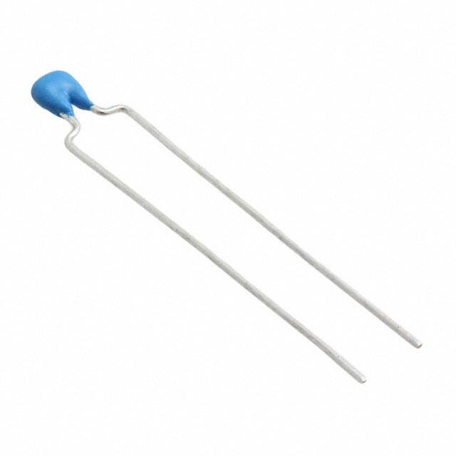


 工商网监
湘ICP备2023018690号
工商网监
湘ICP备2023018690号
