!Note • Please read rating and !CAUTION (for storage, operating, rating, soldering, mounting and handling) in this catalog to prevent smoking and/or burning, etc.
• This catalog has only typical specifications because there is no space for detailed specifications. Therefore, please review our product specifications or consult the approval sheet for product specifications before ordering.
Radial Lead Type
Monolithic Ceramic
Capacitors
Cat.No.C49E-21
C49E.pdf
May.10,2011
�!Note • Please read rating and !CAUTION (for storage, operating, rating, soldering, mounting and handling) in this catalog to prevent smoking and/or burning, etc.
• This catalog has only typical specifications because there is no space for detailed specifications. Therefore, please review our product specifications or consult the approval sheet for product specifications before ordering.
EU RoHS Compliant
•
•
•
All the products in this catalog comply with EU RoHS.
EU RoHS is "the European Directive 2002/95/EC on the Restriction of the Use
of Certain Hazardous Substances in Electrical and Electronic Equipment."
For more details, please refer to our website 'Murata's Approach for EU RoHS'
(http://www.murata.com/info/rohs.html).
C49E.pdf
May.10,2011
�!Note • Please read rating and !CAUTION (for storage, operating, rating, soldering, mounting and handling) in this catalog to prevent smoking and/or burning, etc.
• This catalog has only typical specifications because there is no space for detailed specifications. Therefore, please review our product specifications or consult the approval sheet for product specifications before ordering.
CONTENTS
Part Numbering
1
RPE Series (DC25V-DC100V)
Marking
2
High Dielectric Constant Type, Y5V Characteristics
10
RPE Series Small Size, Large Capacitance (DC50V)
RH Series 150°C max. (for Automotive) (DC50V-DC100V)
Marking
15
16
16
19
20
High Dielectric Constant Type, X8L Characteristics
21
Marking
24
27
28
Temperature Compensating Type, C0G Characteristics
28
High Dielectric Constant Type, X7R/X7S Characteristics
30
High Dielectric Constant Type, F/Y5V Characteristics
33
Specifications and Test Methods
RDE Series Large Capacitance and High Allowable Ripple Current (For Commercial Use Only) (DC250V-DC630V)
Marking
High Dielectric Constant Type, X7T Characteristics
Specifications and Test Methods
Reference Data (Typical Example)
4
17
20
RDE Series (For Commercial Use Only) (DC25V-DC630V)
3
12
Temperature Compensating Type, X8G Characteristics
Specifications and Test Methods
2
5
9
Specifications and Test Methods
5
4
High Dielectric Constant Type, X7R Characteristics
High Dielectric Constant Type, X7R Characteristics
4
2
6
Marking
3
1
Temperature Compensating Type, C0G Characteristics
Specifications and Test Methods
C49E.pdf
May.10,2011
34
37
38
38
40
42
RPE Series
42
RPE Series Small Size, Large Capacitance
43
RH Series
44
RDE Series
45
Packaging
46
!Caution
48
Notice
51
5
�!Note • Please read rating and !CAUTION (for storage, operating, rating, soldering, mounting and handling) in this catalog to prevent smoking and/or burning, etc.
• This catalog has only typical specifications because there is no space for detailed specifications. Therefore, please review our product specifications or consult the approval sheet for product specifications before ordering.
o Part Numbering
Radial Lead Type Monolithic Ceramic Capacitors
(Part Number)
RP
E
R7 1H
q
w
e
104
r
t
2
M1
y u
K
i
A03 A
o
!0
qProduct ID
wSeries/Terminal
Product ID
Series/Terminal
RP
E
RH
E/D
RD
E
Radial Lead Type Monolithic Ceramic Capacitors (DC25V-DC100V)
Radial Lead Type Monolithic Ceramic Capacitors 150°C max. (for Automotive) (DC50V-DC100V)
Radial Lead Type Monolithic Ceramic Capacitors (For Commercial Use Only) (DC25V-DC630V)
eTemperature Characteristics
Code
Temperature
Characteristics
Reference
Temperature
Temperature
Range
Capacitance Change or
Temperature Coefficient
Operating
Temperature Range
5C
C0G*
25°C
25 to 125°C
0±30ppm/°C
-55 to 125°C
5G
X8G*
25°C
25 to 150°C
0±30ppm/°C
-55 to 150°C
C7
X7S
25°C
-55 to 125°C
±22%
-55 to 125°C
D7
X7T
25°C
-55 to 125°C
+22, -33%
-55 to 125°C
F1
F
20°C
-25 to 85°C
+30, -80%
-25 to 85°C
F5
Y5V
25°C
-30 to 85°C
+22, -82%
-30 to 85°C
L8
X8L
25°C
R7
X7R
25°C
-55 to 125°C
±15%
125 to 150°C
+15, -40%
-55 to 125°C
±15%
-55 to 150°C
-55 to 125°C
* Please refer to table for Capacitance change under reference temperature.
• Capacitance change from each temperature
Capacitance Change from 25˚C (%)
Char.
C0G
X8G
Nominal Values (ppm/˚C) *1
0±30
-30˚C
-55˚C
-10˚C
Max.
Min.
Max.
Min.
Max.
Min.
0.58
-0.24
0.40
-0.17
0.25
-0.11
*1: Nominal values denote the temperature coefficient within a range of 25 to 125˚C.
rRated Voltage
yCapacitance Tolerance
Code
Rated Voltage
1E
DC25V
1H
DC50V
C
±0.25pF
2A
DC100V
D
±0.5pF
2E
DC250V
J
±5%
C0G/X8G
U10 : E12 Series
2W
DC450V
2J
DC630V
K
±10%
X7S/X7T/X7R/
X8L
E6 Series
tCapacitance
M
±20%
X7S/X7T/X7R/
X8L
E3 Series
Expressed by three-digit alphanumerics. The unit is pico-farad
(pF). The first and second figures are significant digits, and the
third figure expresses the number of zeros that follow the two
numbers.
If there is a decimal point, it is expressed by the capital letter "R."
In this case, all figures are significant digits.
Z
+80%, -20%
F/Y5V
E3 Series
Code
Capacitance Temperature
Tolerance Characteristics
C0G
Capacitance
Step
V5pF : 1pF Step
6 to 9pF : 1pF Step
Continued on the following page.
2
C49E.pdf
May.10,2011
�!Note • Please read rating and !CAUTION (for storage, operating, rating, soldering, mounting and handling) in this catalog to prevent smoking and/or burning, etc.
• This catalog has only typical specifications because there is no space for detailed specifications. Therefore, please review our product specifications or consult the approval sheet for product specifications before ordering.
C49E.pdf
May.10,2011
Continued from the preceding page.
oIndividual Specification Code
uDimensions (LxW)
Expressed by three-digit alphanumerics
Code
Dimensions (LxW)
0
4.0g3.5mm or 5.0g3.5mm (Depends on Part Number List)
1
4.0g3.5mm or 4.5g3.5mm or 5.0g3.5mm (Depends on Part Number List)
!0Packaging
2
5.0g3.5mm or 5.5g4.0mm or 5.7g4.5mm (Depends on Part Number List)
Code
Packaging
3
5.0g4.5mm or 5.5g5.0mm or 6.0g5.5mm (Depends on Part Number List)
A
Ammo Pack
5
7.5g7.5mm*
B
Bulk
6
10.0g10.0mm
7
12.5g12.5mm
8
7.5g5.5mm
U
7.7g12.5mm*
W
5.5g7.5mm
* DC630V: W+0.5mm
iLead Style
Code
Lead Style
Lead Spacing
A2
Straight Long
2.5mm
B1
Straight Long
5.0mm
C1
Straight Long
10.0mm
DB
Straight Taping
2.5mm
E1/E2
Straight Taping
5.0mm
K1
Inside Crimp
5.0mm
M1/M2
Inside Crimp Taping
5.0mm
P1
Outside Crimp
2.5mm
S1/S2
Outside Crimp Taping
2.5mm
Lead distance between reference and bottom planes.
M1, S1: H0 = 16.0±0.5mm
M2, S2: H0 = 20.0±0.5mm
E1: H = 17.5±0.5mm
E2: H = 20.0±0.5mm
3
�!Note • Please read rating and !CAUTION (for storage, operating, rating, soldering, mounting and handling) in this catalog to prevent smoking and/or burning, etc.
• This catalog has only typical specifications because there is no space for detailed specifications. Therefore, please review our product specifications or consult the approval sheet for product specifications before ordering.
C49E.pdf
May.10,2011
Radial Lead Type Monolithic Ceramic Capacitors
1
RPE Series (DC25V-DC100V)
L max.
25.0 min.
W1 max.
∗
ød : 0.5±0.05
F±0.8
Dimensions code: 2/3
Lead style code: P1
∗ Coating extension does not exceed the end of the lead bend.
· Lead Wire : Solder Coated Copper Wire or
(in mm)
Solder Coated CP Wire
T max.
25.0 min.
∗
W max.
L max.
W1 max.
1. The RPE series capacitors have small dimensions,
large capacitance, and a capacity volume ratio of
10 micro F/cm cubed, close to that of electrolytic
capacitors. They do not have polarity.
2. Excellent frequency characteristics and due to
their small internal inductance are suitable for
high frequencies.
3. Not coated with wax so there is no change in
their exterior appearance due to the outflow of
wax during soldering or solvent during cleansing.
4. They are highly nonflammable, having characteristics
equivalent to the UL94V-0 standard.
W max.
■ Features
T max.
ød : 0.5±0.05
F±0.8
Dimensions code: 2/3/8
Lead style code: K1
∗ Coating extension does not exceed the end of the lead bend.
· Lead Wire : Solder Coated Copper Wire or
(in mm)
Solder Coated CP Wire
■ Dimensions
W
3.5
Dimensions (mm)
W1
T
5.0
F
2.5
d
0.5
2K1/2M1/2M2
5.0
3.5
5.0
5.0
0.5
3P1/3S1/3S2
5.0
4.5
6.3
2.5
0.5
3K1/3M1/3M2
5B1/5E1/5E2
5.0
7.5
4.5
7.5
6.3
-
5.0
5.0
0.5
0.5
6B1/6E1/6E2
10.0
10.0
-
5.0
0.5
7C1
12.5
12.5
-
10.0
0.5
8K1/8M1/8M2
7.5
5.5
8.0
5.0
0.5
See
the individual
product
specifications
W max.
2P1/2S1/2S2
L
5.0
Dimensions and
Lead Style Code
T max.
25.0 min.
1.5 max.
L max.
ød : 0.5±0.05
F±0.8
Dimensions code: 5/6/7
Lead style code: B1/C1
· Lead Wire : Solder Coated Copper Wire or
Solder Coated CP Wire
(in mm)
Continued on the following page.
4
�!Note • Please read rating and !CAUTION (for storage, operating, rating, soldering, mounting and handling) in this catalog to prevent smoking and/or burning, etc.
• This catalog has only typical specifications because there is no space for detailed specifications. Therefore, please review our product specifications or consult the approval sheet for product specifications before ordering.
C49E.pdf
May.10,2011
Continued from the preceding page.
■ Marking
Type
Temperature Compensating Type
Temp. Char.
Dimensions
Code
Individual
Specification
Code
App
Bpp
Zpp
2
Individual
Specification
Code
Except
App
Bpp
Zpp
C0G
102J
5A
1
High Dielectric Constant Type
X7R
Y5V
222K
224Z
Marked on both sides
M
682
J5A
3, 8
—
5, 6, 7
—
M
224
K5C
M 684
K5C
M
474
Z5F
—
M
Temperature Characteristics
Nominal Capacitance
Capacitance Tolerance
225
K5C
—
Marked with code (C0G char.: A, X7R char.: C, Y5V char.: F)
A part is omitted (Please refer to the marking example.)
Under 100pF: Actual value
100pF and over: marked with 3 figures
Marked with code
Rated Voltage
Marked with code (DC25V: 2, DC50V: 5, DC100V: 1)
A part is omitted (Please refer to the marking example.)
Manufacturer's Identification
Marked with M
A part is omitted (Please refer to the marking example.)
5
�!Note • Please read rating and !CAUTION (for storage, operating, rating, soldering, mounting and handling) in this catalog to prevent smoking and/or burning, etc.
• This catalog has only typical specifications because there is no space for detailed specifications. Therefore, please review our product specifications or consult the approval sheet for product specifications before ordering.
1
C49E.pdf
May.10,2011
Temperature Compensating Type, C0G Characteristics
Part Number
Temp.
Char.
Rated
Voltage
(Vdc)
Capacitance
(pF)
Dimensions Dimension
LxW
T
(mm)
(mm)
Lead
Space F
(mm)
Lead Style
Code
Bulk
Lead Style
Code
Taping (1)
Lead Style
Code
Taping (2)
RPE5C1H1R0C2ppB03p
C0G
50
1.0 ±0.25pF
5.0 x 3.5
2.5
2.5
P1
S1
S2
RPE5C1H1R0C2ppB03p
C0G
50
1.0 ±0.25pF
RPE5C1H2R0C2ppB03p
C0G
50
2.0 ±0.25pF
5.0 x 3.5
2.5
5.0
K1
M1
M2
5.0 x 3.5
2.5
2.5
P1
S1
RPE5C1H2R0C2ppB03p
C0G
50
S2
2.0 ±0.25pF
5.0 x 3.5
2.5
5.0
K1
M1
M2
RPE5C1H3R0C2ppB03p
C0G
RPE5C1H3R0C2ppB03p
C0G
50
3.0 ±0.25pF
5.0 x 3.5
2.5
2.5
P1
S1
S2
50
3.0 ±0.25pF
5.0 x 3.5
2.5
5.0
K1
M1
M2
RPE5C1H4R0C2ppB03p
RPE5C1H4R0C2ppB03p
C0G
50
4.0 ±0.25pF
5.0 x 3.5
2.5
2.5
P1
S1
S2
C0G
50
4.0 ±0.25pF
5.0 x 3.5
2.5
5.0
K1
M1
M2
RPE5C1H5R0C2ppB03p
C0G
50
5.0 ±0.25pF
5.0 x 3.5
2.5
2.5
P1
S1
S2
RPE5C1H5R0C2ppB03p
C0G
50
5.0 ±0.25pF
5.0 x 3.5
2.5
5.0
K1
M1
M2
RPE5C1H6R0D2ppB03p
C0G
50
6.0 ±0.5pF
5.0 x 3.5
2.5
2.5
P1
S1
S2
RPE5C1H6R0D2ppB03p
C0G
50
6.0 ±0.5pF
5.0 x 3.5
2.5
5.0
K1
M1
M2
RPE5C1H7R0D2ppZ03p
C0G
50
7.0 ±0.5pF
5.0 x 3.5
2.5
2.5
P1
S1
S2
RPE5C1H7R0D2ppZ03p
C0G
50
7.0 ±0.5pF
5.0 x 3.5
2.5
5.0
K1
M1
M2
RPE5C1H8R0D2ppZ03p
C0G
50
8.0 ±0.5pF
5.0 x 3.5
2.5
2.5
P1
S1
S2
RPE5C1H8R0D2ppZ03p
C0G
50
8.0 ±0.5pF
5.0 x 3.5
2.5
5.0
K1
M1
M2
RPE5C1H9R0D2ppZ03p
C0G
50
9.0 ±0.5pF
5.0 x 3.5
2.5
2.5
P1
S1
S2
RPE5C1H9R0D2ppZ03p
C0G
50
9.0 ±0.5pF
5.0 x 3.5
2.5
5.0
K1
M1
M2
RPE5C1H100J2ppZ03p
C0G
50
10 ±5%
5.0 x 3.5
2.5
2.5
P1
S1
S2
RPE5C1H100J2ppZ03p
C0G
50
10 ±5%
5.0 x 3.5
2.5
5.0
K1
M1
M2
RPE5C1H120J2ppZ03p
C0G
50
12 ±5%
5.0 x 3.5
2.5
2.5
P1
S1
S2
RPE5C1H120J2ppZ03p
C0G
50
12 ±5%
5.0 x 3.5
2.5
5.0
K1
M1
M2
RPE5C1H150J2ppZ03p
C0G
50
15 ±5%
5.0 x 3.5
2.5
2.5
P1
S1
S2
RPE5C1H150J2ppZ03p
C0G
50
15 ±5%
5.0 x 3.5
2.5
5.0
K1
M1
M2
RPE5C1H180J2ppZ03p
C0G
50
18 ±5%
5.0 x 3.5
2.5
2.5
P1
S1
S2
RPE5C1H180J2ppZ03p
C0G
50
18 ±5%
5.0 x 3.5
2.5
5.0
K1
M1
M2
RPE5C1H220J2ppZ03p
C0G
50
22 ±5%
5.0 x 3.5
2.5
2.5
P1
S1
S2
RPE5C1H220J2ppZ03p
C0G
50
22 ±5%
5.0 x 3.5
2.5
5.0
K1
M1
M2
RPE5C1H270J2ppZ03p
C0G
50
27 ±5%
5.0 x 3.5
2.5
2.5
P1
S1
S2
RPE5C1H270J2ppZ03p
C0G
50
27 ±5%
5.0 x 3.5
2.5
5.0
K1
M1
M2
RPE5C1H330J2ppZ03p
C0G
50
33 ±5%
5.0 x 3.5
2.5
2.5
P1
S1
S2
RPE5C1H330J2ppZ03p
C0G
50
33 ±5%
5.0 x 3.5
2.5
5.0
K1
M1
M2
RPE5C1H390J2ppZ03p
C0G
50
39 ±5%
5.0 x 3.5
2.5
2.5
P1
S1
S2
RPE5C1H390J2ppZ03p
C0G
50
39 ±5%
5.0 x 3.5
2.5
5.0
K1
M1
M2
RPE5C1H470J2ppZ03p
C0G
50
47 ±5%
5.0 x 3.5
2.5
2.5
P1
S1
S2
RPE5C1H470J2ppZ03p
C0G
50
47 ±5%
5.0 x 3.5
2.5
5.0
K1
M1
M2
RPE5C1H560J2ppZ03p
C0G
50
56 ±5%
5.0 x 3.5
2.5
2.5
P1
S1
S2
RPE5C1H560J2ppZ03p
C0G
50
56 ±5%
5.0 x 3.5
2.5
5.0
K1
M1
M2
RPE5C1H680J2ppZ03p
C0G
50
68 ±5%
5.0 x 3.5
2.5
2.5
P1
S1
S2
RPE5C1H680J2ppZ03p
C0G
50
68 ±5%
5.0 x 3.5
2.5
5.0
K1
M1
M2
RPE5C1H820J2ppZ03p
C0G
50
82 ±5%
5.0 x 3.5
2.5
2.5
P1
S1
S2
RPE5C1H820J2ppZ03p
C0G
50
82 ±5%
5.0 x 3.5
2.5
5.0
K1
M1
M2
RPE5C1H101J2ppA03p
C0G
50
100 ±5%
5.0 x 3.5
2.5
2.5
P1
S1
S2
RPE5C1H101J2ppA03p
C0G
50
100 ±5%
5.0 x 3.5
2.5
5.0
K1
M1
M2
RPE5C1H121J2ppA03p
C0G
50
120 ±5%
5.0 x 3.5
2.5
2.5
P1
S1
S2
RPE5C1H121J2ppA03p
C0G
50
120 ±5%
5.0 x 3.5
2.5
5.0
K1
M1
M2
RPE5C1H151J2ppA03p
C0G
50
150 ±5%
5.0 x 3.5
2.5
2.5
P1
S1
S2
RPE5C1H151J2ppA03p
C0G
50
150 ±5%
5.0 x 3.5
2.5
5.0
K1
M1
M2
RPE5C1H181J2ppA03p
C0G
50
180 ±5%
5.0 x 3.5
2.5
2.5
P1
S1
S2
RPE5C1H181J2ppA03p
C0G
50
180 ±5%
5.0 x 3.5
2.5
5.0
K1
M1
M2
RPE5C1H221J2ppA03p
C0G
50
220 ±5%
5.0 x 3.5
2.5
2.5
P1
S1
S2
RPE5C1H221J2ppA03p
C0G
50
220 ±5%
5.0 x 3.5
2.5
5.0
K1
M1
M2
RPE5C1H271J2ppA03p
C0G
50
270 ±5%
5.0 x 3.5
2.5
2.5
P1
S1
S2
RPE5C1H271J2ppA03p
C0G
50
270 ±5%
5.0 x 3.5
2.5
5.0
K1
M1
M2
Continued on the following page.
6
�!Note • Please read rating and !CAUTION (for storage, operating, rating, soldering, mounting and handling) in this catalog to prevent smoking and/or burning, etc.
• This catalog has only typical specifications because there is no space for detailed specifications. Therefore, please review our product specifications or consult the approval sheet for product specifications before ordering.
C49E.pdf
May.10,2011
Continued from the preceding page.
Part Number
Temp.
Char.
Rated
Voltage
(Vdc)
Capacitance
(pF)
Dimensions Dimension
LxW
T
(mm)
(mm)
Lead
Space F
(mm)
Lead Style
Code
Bulk
Lead Style
Code
Taping (1)
Lead Style
Code
Taping (2)
RPE5C1H331J2ppA03p
C0G
50
330 ±5%
5.0 x 3.5
2.5
2.5
P1
S1
S2
RPE5C1H331J2ppA03p
C0G
50
330 ±5%
5.0 x 3.5
2.5
5.0
K1
M1
M2
RPE5C1H391J2ppA03p
C0G
50
390 ±5%
5.0 x 3.5
2.5
2.5
P1
S1
S2
RPE5C1H391J2ppA03p
C0G
50
390 ±5%
5.0 x 3.5
2.5
5.0
K1
M1
M2
RPE5C1H471J2ppA03p
C0G
50
470 ±5%
5.0 x 3.5
2.5
2.5
P1
S1
S2
RPE5C1H471J2ppA03p
C0G
50
470 ±5%
5.0 x 3.5
2.5
5.0
K1
M1
M2
RPE5C1H561J2ppA03p
C0G
50
560 ±5%
5.0 x 3.5
2.5
2.5
P1
S1
S2
RPE5C1H561J2ppA03p
C0G
50
560 ±5%
5.0 x 3.5
2.5
5.0
K1
M1
M2
RPE5C1H681J2ppA03p
C0G
50
680 ±5%
5.0 x 3.5
2.5
2.5
P1
S1
S2
RPE5C1H681J2ppA03p
C0G
50
680 ±5%
5.0 x 3.5
2.5
5.0
K1
M1
M2
RPE5C1H821J2ppA03p
C0G
50
820 ±5%
5.0 x 3.5
2.5
2.5
P1
S1
S2
RPE5C1H821J2ppA03p
C0G
50
820 ±5%
5.0 x 3.5
2.5
5.0
K1
M1
M2
RPE5C1H102J2ppA03p
C0G
50
1000 ±5%
5.0 x 3.5
2.5
2.5
P1
S1
S2
RPE5C1H102J2ppA03p
C0G
50
1000 ±5%
5.0 x 3.5
2.5
5.0
K1
M1
M2
RPE5C1H122J2ppA03p
C0G
50
1200 ±5%
5.0 x 3.5
3.15
2.5
P1
S1
S2
RPE5C1H122J2ppA03p
C0G
50
1200 ±5%
5.0 x 3.5
3.15
5.0
K1
M1
M2
RPE5C1H152J2ppA03p
C0G
50
1500 ±5%
5.0 x 3.5
3.15
2.5
P1
S1
S2
RPE5C1H152J2ppA03p
C0G
50
1500 ±5%
5.0 x 3.5
3.15
5.0
K1
M1
M2
RPE5C1H182J2ppC03p
C0G
50
1800 ±5%
5.0 x 3.5
3.15
2.5
P1
S1
S2
RPE5C1H182J2ppA03p
C0G
50
1800 ±5%
5.0 x 3.5
3.15
5.0
K1
M1
M2
RPE5C1H222J2ppC03p
C0G
50
2200 ±5%
5.0 x 3.5
3.15
2.5
P1
S1
S2
RPE5C1H222J2ppA03p
C0G
50
2200 ±5%
5.0 x 3.5
3.15
5.0
K1
M1
M2
RPE5C1H272J2ppC03p
C0G
50
2700 ±5%
5.0 x 3.5
3.15
2.5
P1
S1
S2
RPE5C1H272J2ppA03p
C0G
50
2700 ±5%
5.0 x 3.5
3.15
5.0
K1
M1
M2
RPE5C1H332J2ppC03p
C0G
50
3300 ±5%
5.0 x 3.5
3.15
2.5
P1
S1
S2
RPE5C1H332J2ppA03p
C0G
50
3300 ±5%
5.0 x 3.5
3.15
5.0
K1
M1
M2
RPE5C1H392J2ppC03p
C0G
50
3900 ±5%
5.0 x 3.5
3.15
2.5
P1
S1
S2
RPE5C1H392J2ppA03p
C0G
50
3900 ±5%
5.0 x 3.5
3.15
5.0
K1
M1
M2
RPE5C1H472J2ppC03p
C0G
50
4700 ±5%
5.0 x 3.5
3.15
2.5
P1
S1
S2
RPE5C1H472J2ppA03p
C0G
50
4700 ±5%
5.0 x 3.5
3.15
5.0
K1
M1
M2
RPE5C1H562J2ppC03p
C0G
50
5600 ±5%
5.0 x 3.5
3.15
2.5
P1
S1
S2
RPE5C1H562J2ppA03p
C0G
50
5600 ±5%
5.0 x 3.5
3.15
5.0
K1
M1
M2
RPE5C1H682J2ppC03p
C0G
50
6800 ±5%
5.0 x 3.5
3.15
5.0
K1
M1
M2
RPE5C1H822J2ppC03p
C0G
50
8200 ±5%
5.0 x 3.5
3.15
5.0
K1
M1
M2
RPE5C1H103J2ppC03p
C0G
50
10000 ±5%
5.0 x 3.5
3.15
5.0
K1
M1
M2
RPE5C2A1R0C2ppB03p
C0G
100
1.0 ±0.25pF
5.0 x 3.5
2.5
2.5
P1
S1
S2
RPE5C2A1R0C2ppB03p
C0G
100
1.0 ±0.25pF
5.0 x 3.5
2.5
5.0
K1
M1
M2
RPE5C2A2R0C2ppB03p
C0G
100
2.0 ±0.25pF
5.0 x 3.5
2.5
2.5
P1
S1
S2
RPE5C2A2R0C2ppB03p
C0G
100
2.0 ±0.25pF
5.0 x 3.5
2.5
5.0
K1
M1
M2
RPE5C2A3R0C2ppB03p
C0G
100
3.0 ±0.25pF
5.0 x 3.5
2.5
2.5
P1
S1
S2
RPE5C2A3R0C2ppB03p
C0G
100
3.0 ±0.25pF
5.0 x 3.5
2.5
5.0
K1
M1
M2
RPE5C2A4R0C2ppB03p
C0G
100
4.0 ±0.25pF
5.0 x 3.5
2.5
2.5
P1
S1
S2
RPE5C2A4R0C2ppB03p
C0G
100
4.0 ±0.25pF
5.0 x 3.5
2.5
5.0
K1
M1
M2
RPE5C2A5R0C2ppB03p
C0G
100
5.0 ±0.25pF
5.0 x 3.5
2.5
2.5
P1
S1
S2
RPE5C2A5R0C2ppB03p
C0G
100
5.0 ±0.25pF
5.0 x 3.5
2.5
5.0
K1
M1
M2
RPE5C2A6R0D2ppB03p
C0G
100
6.0 ±0.5pF
5.0 x 3.5
2.5
2.5
P1
S1
S2
RPE5C2A6R0D2ppB03p
C0G
100
6.0 ±0.5pF
5.0 x 3.5
2.5
5.0
K1
M1
M2
RPE5C2A7R0D2ppZ03p
C0G
100
7.0 ±0.5pF
5.0 x 3.5
2.5
2.5
P1
S1
S2
RPE5C2A7R0D2ppZ03p
C0G
100
7.0 ±0.5pF
5.0 x 3.5
2.5
5.0
K1
M1
M2
RPE5C2A8R0D2ppZ03p
C0G
100
8.0 ±0.5pF
5.0 x 3.5
2.5
2.5
P1
S1
S2
RPE5C2A8R0D2ppZ03p
C0G
100
8.0 ±0.5pF
5.0 x 3.5
2.5
5.0
K1
M1
M2
RPE5C2A9R0D2ppZ03p
C0G
100
9.0 ±0.5pF
5.0 x 3.5
2.5
2.5
P1
S1
S2
RPE5C2A9R0D2ppZ03p
C0G
100
9.0 ±0.5pF
5.0 x 3.5
2.5
5.0
K1
M1
M2
RPE5C2A100J2ppZ03p
C0G
100
10 ±5%
5.0 x 3.5
2.5
2.5
P1
S1
S2
RPE5C2A100J2ppZ03p
C0G
100
10 ±5%
5.0 x 3.5
2.5
5.0
K1
M1
M2
RPE5C2A120J2ppZ03p
C0G
100
12 ±5%
5.0 x 3.5
2.5
2.5
P1
S1
S2
RPE5C2A120J2ppZ03p
C0G
100
12 ±5%
5.0 x 3.5
2.5
5.0
K1
M1
M2
1
Continued on the following page.
7
�!Note • Please read rating and !CAUTION (for storage, operating, rating, soldering, mounting and handling) in this catalog to prevent smoking and/or burning, etc.
• This catalog has only typical specifications because there is no space for detailed specifications. Therefore, please review our product specifications or consult the approval sheet for product specifications before ordering.
C49E.pdf
May.10,2011
Continued from the preceding page.
1
Part Number
Temp.
Char.
Rated
Voltage
(Vdc)
Capacitance
(pF)
Dimensions Dimension
LxW
T
(mm)
(mm)
Lead
Space F
(mm)
RPE5C2A150J2ppZ03p
C0G
100
15 ±5%
5.0 x 3.5
2.5
2.5
P1
S1
S2
RPE5C2A150J2ppZ03p
C0G
100
15 ±5%
5.0 x 3.5
2.5
5.0
K1
M1
M2
RPE5C2A180J2ppZ03p
C0G
100
18 ±5%
5.0 x 3.5
2.5
2.5
P1
S1
S2
RPE5C2A180J2ppZ03p
C0G
100
18 ±5%
5.0 x 3.5
2.5
5.0
K1
M1
M2
RPE5C2A220J2ppZ03p
C0G
100
22 ±5%
5.0 x 3.5
2.5
2.5
P1
S1
S2
RPE5C2A220J2ppZ03p
C0G
100
22 ±5%
5.0 x 3.5
2.5
5.0
K1
M1
M2
RPE5C2A270J2ppZ03p
C0G
100
27 ±5%
5.0 x 3.5
2.5
2.5
P1
S1
S2
RPE5C2A270J2ppZ03p
C0G
100
27 ±5%
5.0 x 3.5
2.5
5.0
K1
M1
M2
RPE5C2A330J2ppZ03p
C0G
100
33 ±5%
5.0 x 3.5
2.5
2.5
P1
S1
S2
RPE5C2A330J2ppZ03p
C0G
100
33 ±5%
5.0 x 3.5
2.5
5.0
K1
M1
M2
RPE5C2A390J2ppZ03p
C0G
100
39 ±5%
5.0 x 3.5
2.5
2.5
P1
S1
S2
RPE5C2A390J2ppZ03p
C0G
100
39 ±5%
5.0 x 3.5
2.5
5.0
K1
M1
M2
RPE5C2A470J2ppZ03p
C0G
100
47 ±5%
5.0 x 3.5
2.5
2.5
P1
S1
S2
RPE5C2A470J2ppZ03p
C0G
100
47 ±5%
5.0 x 3.5
2.5
5.0
K1
M1
M2
RPE5C2A560J2ppZ03p
C0G
100
56 ±5%
5.0 x 3.5
2.5
2.5
P1
S1
S2
RPE5C2A560J2ppZ03p
C0G
100
56 ±5%
5.0 x 3.5
2.5
5.0
K1
M1
M2
RPE5C2A680J2ppZ03p
C0G
100
68 ±5%
5.0 x 3.5
2.5
2.5
P1
S1
S2
RPE5C2A680J2ppZ03p
C0G
100
68 ±5%
5.0 x 3.5
2.5
5.0
K1
M1
M2
RPE5C2A820J2ppZ03p
C0G
100
82 ±5%
5.0 x 3.5
2.5
2.5
P1
S1
S2
RPE5C2A820J2ppZ03p
C0G
100
82 ±5%
5.0 x 3.5
2.5
5.0
K1
M1
M2
RPE5C2A101J2ppA03p
C0G
100
100 ±5%
5.0 x 3.5
2.5
2.5
P1
S1
S2
RPE5C2A101J2ppA03p
C0G
100
100 ±5%
5.0 x 3.5
2.5
5.0
K1
M1
M2
RPE5C2A121J2ppA03p
C0G
100
120 ±5%
5.0 x 3.5
2.5
2.5
P1
S1
S2
RPE5C2A121J2ppA03p
C0G
100
120 ±5%
5.0 x 3.5
2.5
5.0
K1
M1
M2
RPE5C2A151J2ppA03p
C0G
100
150 ±5%
5.0 x 3.5
2.5
2.5
P1
S1
S2
RPE5C2A151J2ppA03p
C0G
100
150 ±5%
5.0 x 3.5
2.5
5.0
K1
M1
M2
RPE5C2A181J2ppA03p
C0G
100
180 ±5%
5.0 x 3.5
2.5
2.5
P1
S1
S2
RPE5C2A181J2ppA03p
C0G
100
180 ±5%
5.0 x 3.5
2.5
5.0
K1
M1
M2
RPE5C2A221J2ppA03p
C0G
100
220 ±5%
5.0 x 3.5
2.5
2.5
P1
S1
S2
RPE5C2A221J2ppA03p
C0G
100
220 ±5%
5.0 x 3.5
2.5
5.0
K1
M1
M2
RPE5C2A271J2ppA03p
C0G
100
270 ±5%
5.0 x 3.5
2.5
2.5
P1
S1
S2
RPE5C2A271J2ppA03p
C0G
100
270 ±5%
5.0 x 3.5
2.5
5.0
K1
M1
M2
RPE5C2A331J2ppA03p
C0G
100
330 ±5%
5.0 x 3.5
2.5
2.5
P1
S1
S2
RPE5C2A331J2ppA03p
C0G
100
330 ±5%
5.0 x 3.5
2.5
5.0
K1
M1
M2
RPE5C2A391J2ppA03p
C0G
100
390 ±5%
5.0 x 3.5
2.5
2.5
P1
S1
S2
RPE5C2A391J2ppA03p
C0G
100
390 ±5%
5.0 x 3.5
2.5
5.0
K1
M1
M2
RPE5C2A471J2ppA03p
C0G
100
470 ±5%
5.0 x 3.5
2.5
2.5
P1
S1
S2
RPE5C2A471J2ppA03p
C0G
100
470 ±5%
5.0 x 3.5
2.5
5.0
K1
M1
M2
RPE5C2A561J2ppA03p
C0G
100
560 ±5%
5.0 x 3.5
2.5
2.5
P1
S1
S2
RPE5C2A561J2ppA03p
C0G
100
560 ±5%
5.0 x 3.5
2.5
5.0
K1
M1
M2
RPE5C2A681J2ppA03p
C0G
100
680 ±5%
5.0 x 3.5
2.5
2.5
P1
S1
S2
RPE5C2A681J2ppA03p
C0G
100
680 ±5%
5.0 x 3.5
2.5
5.0
K1
M1
M2
RPE5C2A821J2ppA03p
C0G
100
820 ±5%
5.0 x 3.5
3.15
2.5
P1
S1
S2
RPE5C2A821J2ppA03p
C0G
100
820 ±5%
5.0 x 3.5
3.15
5.0
K1
M1
M2
RPE5C2A102J2ppA03p
C0G
100
1000 ±5%
5.0 x 3.5
3.15
2.5
P1
S1
S2
RPE5C2A102J2ppA03p
C0G
100
1000 ±5%
5.0 x 3.5
3.15
5.0
K1
M1
M2
RPE5C2A122J2ppA03p
C0G
100
1200 ±5%
5.0 x 3.5
3.15
2.5
P1
S1
S2
RPE5C2A122J2ppA03p
C0G
100
1200 ±5%
5.0 x 3.5
3.15
5.0
K1
M1
M2
RPE5C2A152J2ppA03p
C0G
100
1500 ±5%
5.0 x 3.5
3.15
2.5
P1
S1
S2
RPE5C2A152J2ppA03p
C0G
100
1500 ±5%
5.0 x 3.5
3.15
5.0
K1
M1
M2
Two blank columns are filled with the lead style code. Please refer to the 3 columns on the right for the appropriate code.
The last blank column is filled with the packaging code. (B: bulk, A: ammo pack)
8
Lead Style
Code
Bulk
Lead Style
Code
Taping (1)
Lead Style
Code
Taping (2)
�!Note • Please read rating and !CAUTION (for storage, operating, rating, soldering, mounting and handling) in this catalog to prevent smoking and/or burning, etc.
• This catalog has only typical specifications because there is no space for detailed specifications. Therefore, please review our product specifications or consult the approval sheet for product specifications before ordering.
C49E.pdf
May.10,2011
1
High Dielectric Constant Type, X7R Characteristics
Part Number
Temp.
Char.
Rated
Voltage
(Vdc)
Capacitance
Dimensions Dimension
LxW
T
(mm)
(mm)
Lead
Space F
(mm)
Lead Style
Code
Bulk
Lead Style
Code
Taping (1)
Lead Style
Code
Taping (2)
RPER71E474K2ppA03p
X7R
25
0.47µF ±10%
5.0 x 3.5
3.15
5.0
K1
M1
M2
RPER71E684K2ppC03p
X7R
25
0.68µF ±10%
RPER71E105K2ppC03p
X7R
25
1.0µF ±10%
5.0 x 3.5
3.15
5.0
K1
M1
M2
5.0 x 3.5
3.15
5.0
K1
M1
RPER71E155K3ppC07p
X7R
25
M2
1.5µF ±10%
5.0 x 4.5
3.15
5.0
K1
M1
RPER71E225K3ppC07p
X7R
M2
25
2.2µF ±10%
5.0 x 4.5
3.15
5.0
K1
M1
RPER71H221K2ppA03p
M2
X7R
50
220pF ±10%
5.0 x 3.5
2.5
2.5
P1
S1
S2
RPER71H221K2ppA03p
X7R
50
220pF ±10%
5.0 x 3.5
2.5
5.0
K1
M1
M2
RPER71H331K2ppA03p
X7R
50
330pF ±10%
5.0 x 3.5
2.5
2.5
P1
S1
S2
RPER71H331K2ppA03p
X7R
50
330pF ±10%
5.0 x 3.5
2.5
5.0
K1
M1
M2
RPER71H471K2ppA03p
X7R
50
470pF ±10%
5.0 x 3.5
2.5
2.5
P1
S1
S2
RPER71H471K2ppA03p
X7R
50
470pF ±10%
5.0 x 3.5
2.5
5.0
K1
M1
M2
RPER71H681K2ppA03p
X7R
50
680pF ±10%
5.0 x 3.5
2.5
2.5
P1
S1
S2
RPER71H681K2ppA03p
X7R
50
680pF ±10%
5.0 x 3.5
2.5
5.0
K1
M1
M2
RPER71H102K2ppA03p
X7R
50
1000pF ±10%
5.0 x 3.5
2.5
2.5
P1
S1
S2
RPER71H102K2ppA03p
X7R
50
1000pF ±10%
5.0 x 3.5
2.5
5.0
K1
M1
M2
RPER71H152K2ppA03p
X7R
50
1500pF ±10%
5.0 x 3.5
2.5
2.5
P1
S1
S2
RPER71H152K2ppA03p
X7R
50
1500pF ±10%
5.0 x 3.5
2.5
5.0
K1
M1
M2
RPER71H222K2ppA03p
X7R
50
2200pF ±10%
5.0 x 3.5
2.5
2.5
P1
S1
S2
RPER71H222K2ppA03p
X7R
50
2200pF ±10%
5.0 x 3.5
2.5
5.0
K1
M1
M2
RPER71H332K2ppA03p
X7R
50
3300pF ±10%
5.0 x 3.5
2.5
2.5
P1
S1
S2
RPER71H332K2ppA03p
X7R
50
3300pF ±10%
5.0 x 3.5
2.5
5.0
K1
M1
M2
RPER71H472K2ppA03p
X7R
50
4700pF ±10%
5.0 x 3.5
2.5
2.5
P1
S1
S2
RPER71H472K2ppA03p
X7R
50
4700pF ±10%
5.0 x 3.5
2.5
5.0
K1
M1
M2
RPER71H682K2ppA03p
X7R
50
6800pF ±10%
5.0 x 3.5
2.5
2.5
P1
S1
S2
RPER71H682K2ppA03p
X7R
50
6800pF ±10%
5.0 x 3.5
2.5
5.0
K1
M1
M2
RPER71H103K2ppA03p
X7R
50
10000pF ±10%
5.0 x 3.5
2.5
2.5
P1
S1
S2
RPER71H103K2ppA03p
X7R
50
10000pF ±10%
5.0 x 3.5
2.5
5.0
K1
M1
M2
RPER71H153K2ppA03p
X7R
50
15000pF ±10%
5.0 x 3.5
2.5
2.5
P1
S1
S2
RPER71H153K2ppA03p
X7R
50
15000pF ±10%
5.0 x 3.5
2.5
5.0
K1
M1
M2
RPER71H223K2ppA03p
X7R
50
22000pF ±10%
5.0 x 3.5
2.5
2.5
P1
S1
S2
RPER71H223K2ppA03p
X7R
50
22000pF ±10%
5.0 x 3.5
2.5
5.0
K1
M1
M2
RPER71H333K2ppA03p
X7R
50
33000pF ±10%
5.0 x 3.5
3.15
2.5
P1
S1
S2
RPER71H333K2ppA03p
X7R
50
33000pF ±10%
5.0 x 3.5
3.15
5.0
K1
M1
M2
RPER71H473K2ppA03p
X7R
50
47000pF ±10%
5.0 x 3.5
3.15
2.5
P1
S1
S2
RPER71H473K2ppA03p
X7R
50
47000pF ±10%
5.0 x 3.5
3.15
5.0
K1
M1
M2
RPER71H683K2ppA03p
X7R
50
68000pF ±10%
5.0 x 3.5
3.15
2.5
P1
S1
S2
RPER71H683K2ppA03p
X7R
50
68000pF ±10%
5.0 x 3.5
3.15
5.0
K1
M1
M2
RPER71H104K2ppA03p
X7R
50
0.10µF ±10%
5.0 x 3.5
3.15
2.5
P1
S1
S2
RPER71H104K2ppA03p
X7R
50
0.10µF ±10%
5.0 x 3.5
3.15
5.0
K1
M1
M2
RPER71H154K2ppC03p
X7R
50
0.15µF ±10%
5.0 x 3.5
3.15
2.5
P1
S1
S2
RPER71H154K2ppC03p
X7R
50
0.15µF ±10%
5.0 x 3.5
3.15
5.0
K1
M1
M2
RPER71H224K2ppC03p
X7R
50
0.22µF ±10%
5.0 x 3.5
3.15
2.5
P1
S1
S2
RPER71H224K2ppC03p
X7R
50
0.22µF ±10%
5.0 x 3.5
3.15
5.0
K1
M1
M2
RPER71H334K2ppC03p
X7R
50
0.33µF ±10%
5.0 x 3.5
2.5
2.5
P1
S1
S2
RPER71H334K2ppC03p
X7R
50
0.33µF ±10%
5.0 x 3.5
2.5
5.0
K1
M1
M2
RPER71H474K2ppC03p
X7R
50
0.47µF ±10%
5.0 x 3.5
3.15
2.5
P1
S1
S2
RPER71H474K2ppC03p
X7R
50
0.47µF ±10%
5.0 x 3.5
3.15
5.0
K1
M1
M2
RPER71H684K3ppC03p
X7R
50
0.68µF ±10%
5.0 x 4.5
3.15
2.5
P1
S1
S2
RPER71H684K3ppC03p
X7R
50
0.68µF ±10%
5.0 x 4.5
3.15
5.0
K1
M1
M2
RPER71H105K3ppC07p
X7R
50
1.0µF ±10%
5.0 x 4.5
3.15
2.5
P1
S1
S2
RPER71H105K3ppC07p
X7R
50
1.0µF ±10%
5.0 x 4.5
3.15
5.0
K1
M1
M2
RPER71H155K8ppC03p
X7R
50
1.5µF ±10%
7.5 x 5.5
4.0
5.0
K1
M1
M2
RPER71H225K8ppC03p
X7R
50
2.2µF ±10%
7.5 x 5.5
4.0
5.0
K1
M1
M2
RPER71H335K5ppC03p
X7R
50
3.3µF ±10%
7.5 x 7.5
5.0
5.0
B1
E1
E2
Continued on the following page.
9
�!Note • Please read rating and !CAUTION (for storage, operating, rating, soldering, mounting and handling) in this catalog to prevent smoking and/or burning, etc.
• This catalog has only typical specifications because there is no space for detailed specifications. Therefore, please review our product specifications or consult the approval sheet for product specifications before ordering.
C49E.pdf
May.10,2011
Continued from the preceding page.
Rated
Voltage
(Vdc)
Dimensions Dimension
LxW
T
(mm)
(mm)
Lead
Space F
(mm)
Lead Style
Code
Bulk
4.0
5.0
B1
E1
E2
2.5
2.5
P1
S1
S2
5.0 x 3.5
2.5
5.0
K1
M1
M2
5.0 x 3.5
2.5
2.5
P1
S1
S2
330pF ±10%
5.0 x 3.5
2.5
5.0
K1
M1
M2
470pF ±10%
5.0 x 3.5
2.5
2.5
P1
S1
S2
100
470pF ±10%
5.0 x 3.5
2.5
5.0
K1
M1
M2
X7R
100
680pF ±10%
5.0 x 3.5
2.5
2.5
P1
S1
S2
X7R
100
680pF ±10%
5.0 x 3.5
2.5
5.0
K1
M1
M2
RPER72A102K2ppA03p
X7R
100
1000pF ±10%
5.0 x 3.5
2.5
2.5
P1
S1
S2
RPER72A102K2ppA03p
X7R
100
1000pF ±10%
5.0 x 3.5
2.5
5.0
K1
M1
M2
RPER72A152K2ppA03p
X7R
100
1500pF ±10%
5.0 x 3.5
2.5
2.5
P1
S1
S2
RPER72A152K2ppA03p
X7R
100
1500pF ±10%
5.0 x 3.5
2.5
5.0
K1
M1
M2
RPER72A222K2ppA03p
X7R
100
2200pF ±10%
5.0 x 3.5
2.5
2.5
P1
S1
S2
RPER72A222K2ppA03p
X7R
100
2200pF ±10%
5.0 x 3.5
2.5
5.0
K1
M1
M2
RPER72A332K2ppA03p
X7R
100
3300pF ±10%
5.0 x 3.5
2.5
2.5
P1
S1
S2
RPER72A332K2ppA03p
X7R
100
3300pF ±10%
5.0 x 3.5
2.5
5.0
K1
M1
M2
RPER72A472K2ppA03p
X7R
100
4700pF ±10%
5.0 x 3.5
2.5
2.5
P1
S1
S2
RPER72A472K2ppA03p
X7R
100
4700pF ±10%
5.0 x 3.5
2.5
5.0
K1
M1
M2
RPER72A682K2ppA03p
X7R
100
6800pF ±10%
5.0 x 3.5
2.5
2.5
P1
S1
S2
RPER72A682K2ppA03p
X7R
100
6800pF ±10%
5.0 x 3.5
2.5
5.0
K1
M1
M2
RPER72A103K2ppA03p
X7R
100
10000pF ±10%
5.0 x 3.5
3.15
2.5
P1
S1
S2
RPER72A103K2ppA03p
X7R
100
10000pF ±10%
5.0 x 3.5
3.15
5.0
K1
M1
M2
RPER72A153K2ppA03p
X7R
100
15000pF ±10%
5.0 x 3.5
3.15
2.5
P1
S1
S2
RPER72A153K2ppA03p
X7R
100
15000pF ±10%
5.0 x 3.5
3.15
5.0
K1
M1
M2
RPER72A223K2ppA03p
X7R
100
22000pF ±10%
5.0 x 3.5
3.15
2.5
P1
S1
S2
RPER72A223K2ppA03p
X7R
100
22000pF ±10%
5.0 x 3.5
3.15
5.0
K1
M1
M2
RPER72A333K2ppC03p
X7R
100
33000pF ±10%
5.0 x 3.5
3.15
2.5
P1
S1
S2
RPER72A333K2ppC03p
X7R
100
33000pF ±10%
5.0 x 3.5
3.15
5.0
K1
M1
M2
RPER72A473K2ppC03p
X7R
100
47000pF ±10%
5.0 x 3.5
3.15
2.5
P1
S1
S2
RPER72A473K2ppC03p
X7R
100
47000pF ±10%
5.0 x 3.5
3.15
5.0
K1
M1
M2
RPER72A683K3ppC07p
X7R
100
68000pF ±10%
5.0 x 4.5
3.15
2.5
P1
S1
S2
RPER72A683K3ppC07p
X7R
100
68000pF ±10%
5.0 x 4.5
3.15
5.0
K1
M1
M2
RPER72A104K3ppC07p
X7R
100
0.10µF ±10%
5.0 x 4.5
3.15
2.5
P1
S1
S2
RPER72A104K3ppC07p
X7R
100
0.10µF ±10%
5.0 x 4.5
3.15
5.0
K1
M1
M2
RPER72A154K8ppC03p
X7R
100
0.15µF ±10%
7.5 x 5.5
4.0
5.0
K1
M1
M2
RPER72A224K8ppC03p
X7R
100
0.22µF ±10%
7.5 x 5.5
4.0
5.0
K1
M1
M2
RPER72A334K5ppC03p
X7R
100
0.33µF ±10%
7.5 x 7.5
4.0
5.0
B1
E1
E2
RPER72A474K8ppC03p
X7R
100
0.47µF ±10%
7.5 x 5.5
4.0
5.0
K1
M1
M2
RPER72A684K6ppF14p
X7R
100
0.68µF ±10%
10.0 x 10.0
4.0
5.0
B1
E1
E2
RPER72A105K5ppC03p
X7R
100
1.0µF ±10%
7.5 x 7.5
4.0
5.0
B1
E1
E2
RPER72A155K7ppF03p
X7R
100
1.5µF ±10%
12.5 x 12.5
5.0
10.0
C1
-
-
RPER72A225K7ppF03p
X7R
100
2.2µF ±10%
12.5 x 12.5
5.0
10.0
C1
-
-
Lead Style
Code
Bulk
Lead Style
Code
Taping (1)
Lead Style
Code
Taping (2)
Part Number
Temp.
Char.
RPER71H475K5ppC03p
X7R
50
4.7µF ±10%
7.5 x 7.5
RPER72A221K2ppB03p
X7R
100
220pF ±10%
5.0 x 3.5
RPER72A221K2ppB03p
X7R
100
220pF ±10%
RPER72A331K2ppB03p
X7R
100
330pF ±10%
RPER72A331K2ppB03p
X7R
100
RPER72A471K2ppB03p
X7R
100
RPER72A471K2ppB03p
X7R
RPER72A681K2ppB03p
RPER72A681K2ppB03p
1
Capacitance
Lead Style
Code
Taping (1)
Lead Style
Code
Taping (2)
Two blank columns are filled with the lead style code. Please refer to the 3 columns on the right for the appropriate code.
The last blank column is filled with the packaging code. (B: bulk, A: ammo pack)
High Dielectric Constant Type, Y5V Characteristics
Part Number
Temp.
Char.
Rated
Voltage
(Vdc)
Capacitance
Dimensions Dimension
LxW
T
(mm)
(mm)
Lead
Space F
(mm)
RPEF51H102Z2ppA03p
Y5V
50
1000pF +80/-20%
5.0 x 3.5
2.5
2.5
P1
S1
S2
RPEF51H102Z2ppA03p
Y5V
50
1000pF +80/-20%
5.0 x 3.5
2.5
5.0
K1
M1
M2
RPEF51H222Z2ppA03p
Y5V
50
2200pF +80/-20%
5.0 x 3.5
2.5
2.5
P1
S1
S2
RPEF51H222Z2ppA03p
Y5V
50
2200pF +80/-20%
5.0 x 3.5
2.5
5.0
K1
M1
M2
RPEF51H472Z2ppA03p
Y5V
50
4700pF +80/-20%
5.0 x 3.5
2.5
2.5
P1
S1
S2
RPEF51H472Z2ppA03p
Y5V
50
4700pF +80/-20%
5.0 x 3.5
2.5
5.0
K1
M1
M2
Continued on the following page.
10
�!Note • Please read rating and !CAUTION (for storage, operating, rating, soldering, mounting and handling) in this catalog to prevent smoking and/or burning, etc.
• This catalog has only typical specifications because there is no space for detailed specifications. Therefore, please review our product specifications or consult the approval sheet for product specifications before ordering.
C49E.pdf
May.10,2011
Continued from the preceding page.
Part Number
Temp.
Char.
Rated
Voltage
(Vdc)
Capacitance
Dimensions Dimension
LxW
T
(mm)
(mm)
Lead
Space F
(mm)
Lead Style
Code
Bulk
Lead Style
Code
Taping (1)
Lead Style
Code
Taping (2)
RPEF51H103Z2ppA03p
Y5V
50
10000pF +80/-20%
5.0 x 3.5
2.5
2.5
P1
S1
S2
RPEF51H103Z2ppA03p
Y5V
50
10000pF +80/-20%
5.0 x 3.5
2.5
5.0
K1
M1
M2
RPEF51H223Z2ppA03p
Y5V
50
22000pF +80/-20%
5.0 x 3.5
2.5
2.5
P1
S1
S2
RPEF51H223Z2ppA03p
Y5V
50
22000pF +80/-20%
5.0 x 3.5
2.5
5.0
K1
M1
M2
RPEF51H473Z2ppA03p
Y5V
50
47000pF +80/-20%
5.0 x 3.5
2.5
2.5
P1
S1
S2
RPEF51H473Z2ppA03p
Y5V
50
47000pF +80/-20%
5.0 x 3.5
2.5
5.0
K1
M1
M2
RPEF51H104Z2ppA03p
Y5V
50
0.10µF +80/-20%
5.0 x 3.5
2.5
2.5
P1
S1
S2
RPEF51H104Z2ppA03p
Y5V
50
0.10µF +80/-20%
5.0 x 3.5
2.5
5.0
K1
M1
M2
RPEF51H224Z2ppA03p
Y5V
50
0.22µF +80/-20%
5.0 x 3.5
3.15
2.5
P1
S1
S2
RPEF51H224Z2ppA03p
Y5V
50
0.22µF +80/-20%
5.0 x 3.5
3.15
5.0
K1
M1
M2
RPEF51H474Z2ppC03p
Y5V
50
0.47µF +80/-20%
5.0 x 3.5
3.15
2.5
P1
S1
S2
RPEF51H474Z2ppC03p
Y5V
50
0.47µF +80/-20%
5.0 x 3.5
3.15
5.0
K1
M1
M2
Two blank columns are filled with the lead style code. Please refer to the 3 columns on the right for the appropriate code.
The last blank column is filled with the packaging code. (B: bulk, A: ammo pack)
11
1
�C49E.pdf
!Note • Please read rating and !CAUTION (for storage, operating, rating, soldering, mounting and handling) in this catalog to prevent smoking and/or burning, etc.
• This catalog has only typical specifications because there is no space for detailed specifications. Therefore, please review our product specifications or consult the approval sheet for product specifications before ordering.
1
May.10,2011
Specifications and Test Methods
Specifications
No.
Item
Test Method
Temperature Compensating Type High Dielectric Constant Type
1
Operating Temperature
Range
-55 to +125˚C
Char. X7R : -55 to +125˚C
Char. Y5V : -30 to +85˚C
–
2
Rated Voltage
See previous pages
The rated voltage is defined as the maximum voltage
that may be applied continuously to the capacitor.
When AC voltage is superimposed on DC voltage, VP-P
or V0-P, whichever is larger, should be maintained
within the rated voltage range.
3
Appearance
No defects or abnormalities
Visual inspection
4
Dimension and Marking
See previous pages
Visual inspection, Vernier Caliper
No defects or abnormalities
The capacitors should not be damaged when DC
voltages of 300%* of the rated voltage are applied
between the terminals for 1 to 5 sec.
(Charge/Discharge current V 50mA)
*250% for char. X7R, Y5V
No defects or abnormalities
The capacitor is placed in a
container with metal balls of 1mm
diameter so that each terminal,
short-circuited, is kept
approximately 2mm from the balls
as shown in the figure, and 250%
of the rated DC voltage is
impressed for 1 to 5 sec. between
capacitor terminals and metal
balls. (Charge/Discharge current
V 50mA)
Between
Terminals
5
Dielectric
Strength
Body
Insulation
The insulation resistance should be measured with a
DC voltage not exceeding the rated voltage at normal
temperature and humidity and within 2 min. of charging.
(Charge/Discharge current V 50mA)
The capacitance, Q/D.F. should be measured at 25˚C
at the frequency and voltage shown in the table.
6
7
Capacitance
Within the specified tolerance
Q/Dissipation Factor (D.F.)
30pF min. : Q U 1,000
30pF max. : Q U 400+20C
C : Nominal capacitance (pF)
Capacitance
Char. X7R : 0.025 max.
Char. Y5V : 0.05 max.
Item
Frequency
Voltage
Capacitance
Change
9
Within the specified tolerance
(Table A on last column)
Capacitance
Temperature Temperature Within the specified tolerance
Characteristics Coefficient
(Table A on last column)
Within the specified tolerance
(Table B on last column)
Within ±0.2% or ±0.05pF,
whichever is larger
1000pF and
below
more than
1000pF
1±0.1MHz
AC0.5 to 5V
(r.m.s.)
1±0.1kHz
AC1±0.2V
(r.m.s.)
The capacitance change should be measured after 5
min. at each specified temperature stage.
(1) Temperature Compensating Type
The temperature coefficient is determined using the
capacitance measured in step 3 as a reference. When
cycling the temperature sequentially from step 1
through 5 (-55 to +125˚C) the capacitance should be
within the specified tolerance for the temperature
coefficient and capacitance change as shown in Table
A. The capacitance drift is calculated by dividing the
differences between the maximum and minimum
measured values in step 1, 3 and 5 by the cap. value in
step 3.
Step
1
2
3
4
5
Capacitance
Drift
Metal balls
C V 0.047µF : 10,000MΩ min.
C G 0.047µF : 500MΩ • µF min.
C : Nominal capacitance
Insulation
Resistance
8
Between
Terminals
Approx. 2mm
Temperature (°C)
25±2
-55±3
25±2
125±3
25±2
(2) High Dielectric Constant Type
The ranges of capacitance change compared with the
25˚C value over the temperature ranges as shown in
Table B should be within the specified ranges.
Continued on the following page.
12
�C49E.pdf
!Note • Please read rating and !CAUTION (for storage, operating, rating, soldering, mounting and handling) in this catalog to prevent smoking and/or burning, etc.
• This catalog has only typical specifications because there is no space for detailed specifications. Therefore, please review our product specifications or consult the approval sheet for product specifications before ordering.
May.10,2011
Specifications and Test Methods
Continued from the preceding page.
Specifications
No.
Item
Test Method
Temperature Compensating Type High Dielectric Constant Type
As in the figure, fix the capacitor body, apply the force
gradually to each lead in the radial direction of the
capacitor until reaching 10N and then keep the force
applied for 10±1 sec.
Tensile
Strength
10
Termination not to be broken or loosened
Terminal
Strength
F
Bending
Strength
Termination not to be broken or loosened
Appearance No defects or abnormalities
Vibration
11
Resistance
Capacitance
Within the specified tolerance
Q/D.F.
30pF min. : Q U 1,000
30pF max. : Q U 400+20C
C : Nominal capacitance (pF)
12 Solderability of Leads
Char. X7R : 0.025 max.
Char. Y5V : 0.05 max.
Lead wire should be soldered with uniform coating on the axial
direction over 3/4 of the circumferential direction.
Appearance No defects or abnormalities
13
Resistance
to
Soldering
Heat
Capacitance
Change
Within ±2.5% or ±0.25pF
(whichever is larger)
Dielectric
Strength
(Between
Terminals)
No defects
Char. X7R : Within ±7.5%
Char. Y5V : Within ±20%
Temperature
and
Immersion
Cycle
The capacitor is soldered securely to a supporting
terminal and a 10 to 55Hz vibration of 1.5mm peakpeak amplitude is applied for 6 hrs. total, 2 hrs. in each
mutually perpendicular direction. Allow 1 min. to cycle
the frequency from 10Hz to 55Hz and the converse.
The terminal of a capacitor is dipped into a 25% ethanol
(JIS-K-8101) solution of rosin (JIS-K-5902) and
then into molten solder for 2±0.5 sec. In both cases the
depth of dipping is up to about 1.5mm to 2mm from the
terminal body.
Temp. of solder: 245±5˚C Lead Free Solder (Sn-3.0Ag-0.5Cu)
235±5˚C H60A or H63A Eutectic Solder
The lead wire is immersed in the melted solder 1.5mm
to 2mm from the main body at 350±10˚C for 3.5±0.5
sec. The specified items are measured after 24±2 hrs.
(temperature compensating type) or 48±4 hrs. (high
dielectric type).
• Initial measurement for high dielectric constant type
0
The capacitors are heat treated for 1 hr. at 150+
–10 ˚C,
allowed to set at room temperature for 48±4 hrs., and
given an initial measurement.
Appearance No defects or abnormalities
14
Each lead wire should be subjected to a force of 2.5N
and then bent 90˚ at the point of egress in one
direction. Each wire is then returned to the original
position and bent 90˚ in the opposite direction at the
rate of one bend per 2 to 3 sec.
Capacitance
Change
Within ±5% or ±0.5pF
(whichever is larger)
Char. X7R : Within ±12.5%
Char. Y5V : Within ±30%
Q/D.F.
30pF min. : Q U 350
10pF to 30pF : Q U 275+5C/2
10pF max. : Q U 200+10C
C : Nominal capacitance (pF)
Char. X7R : 0.05 max.
Char. Y5V : 0.075 max.
Insulation
Resistance
1,000MΩ or 50MΩ • µF min.
(whichever is smaller)
Dielectric
Strength
(Between
Terminals)
No defects or abnormalities
First, repeat the following temperature/time cycle 5
times:
lowest operating temperature ±3˚C/30±3 min.
ordinary temperature/3 min. max.
highest operating temperature ±3˚C/30±3 min.
ordinary temperature/3 min. max.
Next, repeat twice the successive cycles of immersion,
each cycle consisting of immersion in a fresh water at
65+5
–0˚C for 15 min. and immersion in a saturated
aqueous solution of salt at 0±3˚C for 15 min.
The capacitor is then promptly washed in running
water, dried with a drying cloth, and allowed to sit at
room temperature for 24±2 hrs. (temperature
compensating type) or 48±4 hrs. (high dielectric type).
• Initial measurement for high dielectric constant type
The capacitors are heat treated for 1 hr. at
0
150+–10
˚C, allowed to sit at room temperature for 48
±4 hrs., and given an initial measurement.
Continued on the following page.
13
1
�C49E.pdf
!Note • Please read rating and !CAUTION (for storage, operating, rating, soldering, mounting and handling) in this catalog to prevent smoking and/or burning, etc.
• This catalog has only typical specifications because there is no space for detailed specifications. Therefore, please review our product specifications or consult the approval sheet for product specifications before ordering.
1
May.10,2011
Specifications and Test Methods
Continued from the preceding page.
Specifications
No.
Item
Test Method
Temperature Compensating Type High Dielectric Constant Type
Appearance No defects or abnormalities
Humidity
15 (Steady
State)
Capacitance
Change
Within ±5% or ±0.5pF
(whichever is larger)
Char. X7R : Within ±12.5%
Char. Y5V : Within ±30%
Q/D.F.
30pF min. : Q U 350
10pF to 30pF : Q U 275+5C/2
10pF max. : Q U 200+10C
C : Nominal capacitance (pF)
Char. X7R : 0.05 max.
Char. Y5V : 0.075 max.
Insulation
Resistance
1,000MΩ or 50MΩ • µF min.
(whichever is smaller)
+24
Set the capacitor for 500 –
0 hrs. at 40±2˚C in 90 to
95% humidity. Remove and set for 24±2 hrs.
(temperature compensating type) and 48±4 hrs. (high
dielectric constant type) at room temperature, then
measure.
Appearance No defects or abnormalities
16
Humidity
Load
Capacitance
Change
Within ±7.5% or ±0.75pF
(whichever is larger)
Char. X7R : Within ±12.5%
Char. Y5V : Within ±30%
Q/D.F.
30pF min. : Q U 200
30pF max. : Q U 100+10C/3
C : Nominal capacitance (pF)
Char. X7R : 0.05 max.
Char. Y5V : 0.075 max.
Insulation
Resistance
500MΩ or 25MΩ • µF min.
(whichever is smaller)
Appearance No defects or abnormalities
High
17 Temperature
Load
Capacitance
Change
Within ±3% or ±0.3pF
(whichever is larger)
Char. X7R : Within ±12.5%
Char. Y5V : Within ±30%
Q/D.F.
30pF min. : Q U 350
10pF to 30pF : Q U 275+5C/2
10pF max. : Q U 200+10C
C : Nominal capacitance (pF)
Char. X7R : 0.04 max.
Char. Y5V : 0.075 max.
Insulation
Resistance
Solvent
Resistance
Marking
1,000MΩ or 50MΩ • µF min.
(whichever is smaller)
Table B
Char.
Nominal Values
(ppm/˚C) *1
C0G
0±30
Capacitance Change from 25˚C (%)
-55˚C
-30˚C
-10˚C
Max.
Min.
Max.
Min.
Max.
Min.
0.58
-0.24
0.40
-0.17
0.25
-0.11
*1: Nominal values denote the temperature coefficient within a range of
25 to 125˚C
14
The capacitor should be fully immersed, unagitated, in
reagent at 20 to 25˚C for 30±5 sec. and then removed
gently. Marking on the surface of the capacitor should
immediately be visually examined.
Reagent:
• Isopropyl alcohol
Legible
Table A
+48
Apply 200% of the rated voltage for 1000 –
0 hrs. at
the maximum operating temperature. Remove and set
for 24±2 hrs. (temperature compensating type) and 48
±4 hrs. (high dielectric constant type) at room
temperature, then measure.
(Charge/Discharge current V 50mA)
• Initial measurement for high dielectric constant type
A voltage treatment should be given to the capacitor in
which a DC voltage of 200% of the rated voltage is
applied for 1 hr. at the maximum operating temperature
±3˚C. Then set for 48±4 hrs. at room temperature and
conduct initial measurement.
Appearance No defects or abnormalities
18
Apply the rated voltage for 500 +24
– 0 hrs. at 40±2˚C and
in 90 to 95% humidity. Remove and set for 24±2 hrs.
(temperature compensating type) and 48±4 hrs. (high
dielectric constant type) at room temperature, then
measure.
(Charge/Discharge current V 50mA)
Char.
X7R
Y5V
Temp. Range
-55 to +125˚C
-30 to + 85˚C
Reference Temp.
25˚C
Cap. Change Rate
Within ± 15%
Within +22
–82%
�!Note • Please read rating and !CAUTION (for storage, operating, rating, soldering, mounting and handling) in this catalog to prevent smoking and/or burning, etc.
• This catalog has only typical specifications because there is no space for detailed specifications. Therefore, please review our product specifications or consult the approval sheet for product specifications before ordering.
C49E.pdf
May.10,2011
Radial Lead Type Monolithic Ceramic Capacitors
RPE Series Small Size, Large Capacitance (DC50V)
T max.
25.0 min.
∗
2
ød : 0.5±0.05
F±0.8
Dimensions code: 2/3
Lead style code: K1
∗ Coating extension does not exceed the end of the lead bend.
· Lead Wire : Solder Coated Copper Wire or
(in mm)
Solder Coated CP Wire
W max.
T max.
W1 max.
L max.
25.0 min.
∗
1. The RPE series capacitors have small dimensions,
large capacitance, and a capacity volume ratio of
10 micro F/cm cubed, close to that of electrolytic
capacitors. They do not have polarity.
2. Excellent frequency characteristics and due to
their small internal inductance are suitable for
high frequencies.
3. They are not coated with wax so there is no change
in their exterior appearance due to the outflow of
wax during soldering or solvent during cleansing.
4. They are highly nonflammable, having characteristics
equivalent to the UL94V-0 standard.
5. We design capacitors in much more compact size than
current RPE Series, having reduced the diameter
by 70% max.
W max.
■ Features
W1 max.
L max.
Dimensions code: W
Lead style code: K1
ød : 0.5±0.05
F±0.8
∗ Coating extension does not exceed the end of the lead bend.
· Lead Wire : Solder Coated Copper Wire or
(in mm)
Solder Coated CP Wire
■ Dimensions
Dimensions and
Lead Style Code
Dimensions (mm)
L
W
W1
2K1/2M1
5.5
4.0
6.0
3K1/3M1
5.5
5.0
7.5
WK1/WM1
5.5
7.5
10.0
T
Depends on
Part Number
List
F
d
5.0
0.5
5.0
0.5
5.0
0.5
Continued on the following page.
15
�!Note • Please read rating and !CAUTION (for storage, operating, rating, soldering, mounting and handling) in this catalog to prevent smoking and/or burning, etc.
• This catalog has only typical specifications because there is no space for detailed specifications. Therefore, please review our product specifications or consult the approval sheet for product specifications before ordering.
C49E.pdf
May.10,2011
Continued from the preceding page.
■ Marking
Rated Voltage
Dimensions
Code
DC50V
Temp. Char.
X7R
M
2
225
K5C
2
M 475
3
K5C
M 106
W
M5C
Temperature Characteristics
Marked with code (X7R char.: C)
Marked with 3 figures
Nominal Capacitance
Marked with code
Capacitance Tolerance
Marked with code (DC50V: 5)
Rated Voltage
Marked with
Manufacturer's Identification
M
High Dielectric Constant Type, X7R Characteristics
Part Number
Temp.
Char.
Rated
Voltage
(Vdc)
Capacitance
(µF)
Dimensions Dimension
LxW
T
(mm)
(mm)
Lead
Space F
(mm)
Lead Style
Code
Bulk
Lead Style
Code
Taping (1)
Lead Style
Code
Taping (2)
RPER71H105K2ppC60p
X7R
50
1.0 ±10%
5.5 x 4.0
3.15
5.0
K1
M1
-
RPER71H155K2ppC60p
X7R
50
1.5 ±10%
RPER71H225K2ppC60p
X7R
50
2.2 ±10%
5.5 x 4.0
3.15
5.0
K1
M1
-
5.5 x 4.0
3.15
5.0
K1
M1
RPER71H335K3ppC60p
X7R
50
-
3.3 ±10%
5.5 x 5.0
4.0
5.0
K1
M1
RPER71H475K3ppC60p
X7R
-
50
4.7 ±10%
5.5 x 5.0
4.0
5.0
K1
M1
RPER71H106MWppC60p
X7R
-
50
10 ±20%
5.5 x 7.5
4.0
5.0
K1
M1
-
Two blank columns are filled with the lead style code. Please refer to the 3 columns on the right for the appropriate code.
The last blank column is filled with the packaging code. (B: bulk, A: ammo pack)
16
�C49E.pdf
!Note • Please read rating and !CAUTION (for storage, operating, rating, soldering, mounting and handling) in this catalog to prevent smoking and/or burning, etc.
• This catalog has only typical specifications because there is no space for detailed specifications. Therefore, please review our product specifications or consult the approval sheet for product specifications before ordering.
May.10,2011
RPE Series Small Size, Large Capacitance Specifications
and Test
Specifications
andMethods
Test Methods
No.
Item
Specifications
Test Method
1
Operating Temperature
Range
-55 to +125˚C
2
Appearance
No defects or abnormalities
Visual inspection
3
Dimension and Marking
See previous pages
Visual inspection, Vernier Caliper
No defects or abnormalities
The capacitor should not be damaged when DC
voltage of 250% of the rated voltage is applied
between the terminations for 1 to 5 sec.
(Charge/Discharge current V 50mA)
No defects or abnormalities
The capacitor is placed in a
container with metal balls of 1mm
diameter so that each terminal,
short-circuit, is kept approximately
2mm from the balls as shown in
the figure, and 250% of the rated
DC voltage is impressed for 1 to 5
sec. between capacitor terminals
and metal balls.
(Charge/Discharge current
V 50mA)
Between
Terminals
4
Dielectric
Strength
Body
Insulation
5
Insulation
Resistance
Between
Terminals
6
Capacitance
Within the specified tolerance
7
Dissipation Factor (D.F.)
0.025 max.
500MΩ · µF min.
–
2
Approx. 2mm
Metal balls
The insulation resistance should be measured with a
DC voltage not exceeding the rated voltage at normal
temperature and humidity and within 2 min. of
charging.
(Charge/Discharge current V 50mA)
The capacitance/D.F. should be measured at the
frequency of 1T0.1kHz and a voltage of
AC1T0.2V(r.m.s.)
The capacitance change should be measured after
5 min. at each specified temperature stage.
8
Capacitance
Temperature
Characteristics
Within T15%
Step
1
2
3
4
5
Temperature (˚C)
25T2
-55T3
25T2
125T3
25T2
As in the figure, fix the capacitor body, apply the force
gradually to each lead in the radial direction of the
capacitor until reaching 10N and then keep the force
applied for 10T1 sec.
Tensile
Strength
9
Termination not to be broken or loosened
Terminal
Strength
F
Bending
Strength
Termination not to be broken or loosened
Appearance No defects or abnormalities
10
Vibration
Resistance
Capacitance Within the specified tolerance
D.F.
0.025 max.
Each lead wire should be subjected to a force of 2.5N
and then bent 90˚ at the point of egress in one
direction. Each wire is then returned to the original
position and bent 90˚ in the opposite direction at the
rate of one bend per 2 to 3 sec.
The capacitor should be firmly soldered to the
supporting lead wire and vibrated at a frequency range
of 10 to 55Hz, 1.5mm in total amplitude, with about a 1
minute rate of vibration change from 10Hz to 55Hz and
back to 10Hz. Apply for a total of 6 hrs., 2 hrs. each in 3
mutually perpendicular directions.
Continued on the following page.
17
�!Note • Please read rating and !CAUTION (for storage, operating, rating, soldering, mounting and handling) in this catalog to prevent smoking and/or burning, etc.
• This catalog has only typical specifications because there is no space for detailed specifications. Therefore, please review our product specifications or consult the approval sheet for product specifications before ordering.
C49E.pdf
May.10,2011
RPE Series Small
Capacitance Specifications and Test Methods
Specifications
andSize,
TestLarge
Methods
Continued from the preceding page.
No.
2
Item
11 Solderability of Leads
Specifications
Lead wire should be soldered with uniform coating on the axial
direction over 3/4 of the circumferential direction.
Appearance No defects or abnormalities
Resistance
to
12
Soldering
Heat
Capacitance
Within T7.5%
Change
Dielectric
Strength
(Between
Terminals)
No defects
Test Method
The terminal of a capacitor is dipped into a solution of
ethanol (JIS-K-8101) and rosin (JIS-K-5902) (25% rosin
in weight proportion) and then into molten solder (JISZ-3282) for 2T0.5 sec. In both cases the depth of
dipping is up to about 1.5 to 2mm from the terminal
body.
Temp. of solder: 245T5˚C Lead Free Solder (Sn-3.0Ag-0.5Cu)
235T5˚C H60A or H63A Eutectic Solder
The lead wire is immersed in the melted solder 1.5 to
2mm from the main body at 350T10˚C for 3.5T0.5 sec.
The specified items are measured after 48T4 hrs.
• Pretreatment
Perform a heat treatment at 150+0/-10˚C for 1 hr., and
then let sit at room temperature for 48T4 hrs.
Appearance No defects or abnormalities
Capacitance
Within T12.5%
Change
Temperature
13
Cycle
D.F.
0.05 max.
Insulation
Resistance
50MΩ · µF min.
Dielectric
Strength
(Between
Terminals)
No defects or abnormalities
The capacitor should be subjected to 200 temperature
cycles. (5 temperature cycles for dimensions code W)
Step
1
2
3
4
Temperature (˚C)
-55T3
Room Temp.
125T3
Room Temp.
Time (min)
30T3
3 max.
30T3
3 max.
Appearance No defects or abnormalities
Humidity
14 (Steady
State)
Capacitance
Within T12.5%
Change
D.F.
0.05 max.
Insulation
Resistance
50MΩ · µF min.
Set the capacitor at 40T2˚C and relative humidity of 90
24
to 95% for 500 W
Y 0 hrs. Remove and set for 48T4 hrs.
at room temperature, then measure.
Appearance No defects or abnormalities
Humidity
15
Load
Capacitance
Within T12.5%
Change
D.F.
0.05 max.
Insulation
Resistance
50MΩ · µF min.
Appearance No defects or abnormalities
High
16 Temperature
Load
Capacitance
Within T12.5%
Change
D.F.
0.04 max.
Insulation
Resistance
50MΩ · µF min.
Appearance No defects or abnormalities
17
18
Solvent
Resistance
Marking
Legible
Apply the rated voltage at 40T2˚C and relative humidity
24
of 90 to 95% for 500 W
Y 0 hrs. Remove and set for
48T4 hrs. at room temperature, then measure.
(Charge/Discharge current V 50mA)
Apply a DC voltage of 150% of the rated voltage for
48
1000 W
Y 0 hrs. at the maximum operating temperature.
Remove and set for 48T4 hrs. at room temperature,
then measure.
(Charge/Discharge current V 50mA)
• Pretreatment
Apply test voltage for 1 hr., at test temperature. Remove
and set for 48T4 hrs. at room temperature.
The capacitor should be fully immersed, unagitated, in
reagent at 20 to 25 ˚C for 30T5 sec. and then removed
gently. Marking on the surface of the capacitor should
immediately be visually examined.
Reagent :
• Isopropyl alcohol
�!Note • Please read rating and !CAUTION (for storage, operating, rating, soldering, mounting and handling) in this catalog to prevent smoking and/or burning, etc.
• This catalog has only typical specifications because there is no space for detailed specifications. Therefore, please review our product specifications or consult the approval sheet for product specifications before ordering.
C49E.pdf
May.10,2011
Radial Lead Type Monolithic Ceramic Capacitors
RH Series 150°C max. (for Automotive) (DC50V-DC100V)
L max.
W max.
1.5 max.
■ Features
25.0 min.
1. Small size and large capacitance
2. Low ESR and ESL suitable for high frequency
3. Applied maximum temperature up to 150 deg. C
Note: Maximum accumulative time to 150 deg. C
is within 2000 hours.
4. Coated with epoxy (LxW=4.0x3.5mm) or
silicone (LxW=4.0x3.5mm over) resin which is
suitable for heat cycle.
5. The RH series meet AEC-Q200 requirements.
T max.
ød : 0.5±0.05
3
F±0.8
Dimensions code: 1
Lead style code: A2
· Lead Wire : Solder Coated Copper Wire or
Solder Coated CP Wire
(in mm)
L max.
1.5 max.
ød : 0.5±0.05
F±0.8
Dimensions code: 2
Lead style code: A2
T max.
25.0 min.
25.0 min.
1.5 max.
W max.
T max.
W max.
L max.
ød : 0.5±0.05
F±0.8
Dimensions code: 3
Lead style code: A2
· Lead Wire : Solder Coated Copper Wire or
Solder Coated CP Wire
· Lead Wire : Solder Coated Copper Wire or
Solder Coated CP Wire
(in mm)
W max.
∗
W1 max.
ød : 0.5±0.05
F±0.8
ød : 0.5±0.05
F±0.8
∗ Coating extension does not exceed the end of the lead bend.
· Lead Wire : Solder Coated Copper Wire or
(in mm)
Solder Coated CP Wire
∗ Coating extension does not exceed the end of the lead bend.
· Lead Wire : Solder Coated Copper Wire or
(in mm)
Solder Coated CP Wire
T max.
T max.
W max.
L max.
25.0 min.
25.0 min.
∗
W1 max.
∗
W max.
L max.
Dimensions code: 2
Lead style code: K1
W1 max.
Dimensions code: 1
Lead style code: K1
T max.
25.0 min.
25.0 min.
∗
L max.
W1 max.
T max.
W max.
L max.
(in mm)
ød : 0.5±0.05
ød : 0.5±0.05
F±0.8
Dimensions code: 3
Lead style code: K1
∗ Coating extension does not exceed the end of the lead bend.
· Lead Wire : Solder Coated Copper Wire or
(in mm)
Solder Coated CP Wire
Dimensions code: W
Lead style code: K1
F±0.8
∗ Coating extension does not exceed the end of the lead bend.
· Lead Wire : Solder Coated Copper Wire or
(in mm)
Solder Coated CP Wire
Continued on the following page.
19
�!Note • Please read rating and !CAUTION (for storage, operating, rating, soldering, mounting and handling) in this catalog to prevent smoking and/or burning, etc.
• This catalog has only typical specifications because there is no space for detailed specifications. Therefore, please review our product specifications or consult the approval sheet for product specifications before ordering.
C49E.pdf
May.10,2011
Continued from the preceding page.
■ Dimensions
Dimensions and
Lead Style Code
Dimensions (mm)
L
W
W1
1A2/1DB
4.0
3.5
-
1K1/1M1
4.0
3.5
5.0
2A2/2DB
5.7
4.5
-
2K1/2M1
5.7
4.5
7.0
3A2/3DB
6.0
5.5
-
3K1/3M1
6.0
5.5
WK1/WM1
6.0
8.0
T
F
d
2.5
0.5
5.0
0.5
2.5
0.5
5.0
0.5
2.5
0.5
7.5
5.0
0.5
10.0
5.0
0.5
See
the individual
product
specifications
3
■ Marking
Type
Temperature Compensating Type
Rated Voltage
Dimensions
Code
Temp. Char.
8
102J
2
—
3, W
—
DC100V
DC50V
X8G
1
Temperature Characteristics
High Dielectric Constant Type
DC50V, DC100V
X8L
8
104K
M
8
103K
105
K58
M
335
K58
M
104
K18
—
Marked with code (X8G, X8L char.: 8)
Marked with 3 figures
Nominal Capacitance
Marked with code
Capacitance Tolerance
Rated Voltage
Marked with code (DC50V: 5, DC100V: 1)
A part is omitted (Please refer to the marking example.)
Manufacturer's Identification
Marked with M
A part is omitted (Please refer to the marking example.)
Temperature Compensating Type, X8G Characteristics
Part Number
Temp.
Char.
Rated
Voltage
(Vdc)
Capacitance
(pF)
Dimensions Dimension
LxW
T
(mm)
(mm)
Lead
Space F
(mm)
RHE5G1H101J1ppA03p
X8G
50
100 ±5%
4.0 x 3.5
2.5
2.5
RHE5G1H101J1ppA03p
X8G
50
100 ±5%
4.0 x 3.5
2.5
5.0
RHE5G1H121J1ppA03p
X8G
50
120 ±5%
4.0 x 3.5
2.5
2.5
RHE5G1H121J1ppA03p
X8G
50
120 ±5%
4.0 x 3.5
2.5
5.0
RHE5G1H151J1ppA03p
X8G
50
150 ±5%
4.0 x 3.5
2.5
2.5
RHE5G1H151J1ppA03p
X8G
50
150 ±5%
4.0 x 3.5
2.5
5.0
RHE5G1H181J1ppA03p
X8G
50
180 ±5%
4.0 x 3.5
2.5
2.5
RHE5G1H181J1ppA03p
X8G
50
180 ±5%
4.0 x 3.5
2.5
RHE5G1H221J1ppA03p
X8G
50
220 ±5%
4.0 x 3.5
RHE5G1H221J1ppA03p
X8G
50
220 ±5%
RHE5G1H271J1ppA03p
X8G
50
270 ±5%
RHE5G1H271J1ppA03p
X8G
50
RHE5G1H331J1ppA03p
X8G
RHE5G1H331J1ppA03p
Lead Style
Code
Bulk
Lead Style
Code
Taping (1)
Lead Style
Code
Taping (2)
A2
DB
-
K1
M1
-
A2
DB
-
K1
M1
-
A2
DB
-
K1
M1
-
A2
DB
-
5.0
K1
M1
-
2.5
2.5
A2
DB
-
4.0 x 3.5
2.5
5.0
K1
M1
-
4.0 x 3.5
2.5
2.5
A2
DB
-
270 ±5%
4.0 x 3.5
2.5
5.0
K1
M1
-
50
330 ±5%
4.0 x 3.5
2.5
2.5
A2
DB
-
X8G
50
330 ±5%
4.0 x 3.5
2.5
5.0
K1
M1
-
RHE5G1H391J1ppA03p
X8G
50
390 ±5%
4.0 x 3.5
2.5
2.5
A2
DB
-
RHE5G1H391J1ppA03p
X8G
50
390 ±5%
4.0 x 3.5
2.5
5.0
K1
M1
-
Continued on the following page.
20
�!Note • Please read rating and !CAUTION (for storage, operating, rating, soldering, mounting and handling) in this catalog to prevent smoking and/or burning, etc.
• This catalog has only typical specifications because there is no space for detailed specifications. Therefore, please review our product specifications or consult the approval sheet for product specifications before ordering.
C49E.pdf
May.10,2011
Continued from the preceding page.
Part Number
Temp.
Char.
Rated
Voltage
(Vdc)
Capacitance
(pF)
Dimensions Dimension
LxW
T
(mm)
(mm)
Lead
Space F
(mm)
RHE5G1H471J1ppA03p
X8G
50
470 ±5%
4.0 x 3.5
2.5
2.5
RHE5G1H471J1ppA03p
X8G
50
470 ±5%
4.0 x 3.5
2.5
5.0
RHE5G1H561J1ppA03p
X8G
50
560 ±5%
4.0 x 3.5
2.5
2.5
RHE5G1H561J1ppA03p
X8G
50
560 ±5%
4.0 x 3.5
2.5
5.0
RHE5G1H681J1ppA03p
X8G
50
680 ±5%
4.0 x 3.5
2.5
2.5
RHE5G1H681J1ppA03p
X8G
50
680 ±5%
4.0 x 3.5
2.5
5.0
RHE5G1H821J1ppA03p
X8G
50
820 ±5%
4.0 x 3.5
2.5
2.5
RHE5G1H821J1ppA03p
X8G
50
820 ±5%
4.0 x 3.5
2.5
RHE5G1H102J1ppA03p
X8G
50
1000 ±5%
4.0 x 3.5
RHE5G1H102J1ppA03p
X8G
50
1000 ±5%
RHE5G1H122J1ppA03p
X8G
50
1200 ±5%
RHE5G1H122J1ppA03p
X8G
50
RHE5G1H152J1ppA03p
X8G
RHE5G1H152J1ppA03p
RHE5G2A101J1ppA03p
Lead Style
Code
Bulk
Lead Style
Code
Taping (1)
Lead Style
Code
Taping (2)
A2
DB
-
K1
M1
-
A2
DB
-
K1
M1
-
A2
DB
-
K1
M1
-
A2
DB
-
5.0
K1
M1
-
2.5
2.5
A2
DB
-
4.0 x 3.5
2.5
5.0
K1
M1
-
4.0 x 3.5
2.5
2.5
A2
DB
-
1200 ±5%
4.0 x 3.5
2.5
5.0
K1
M1
-
50
1500 ±5%
4.0 x 3.5
2.5
2.5
A2
DB
-
X8G
50
1500 ±5%
4.0 x 3.5
2.5
5.0
K1
M1
-
X8G
100
100 ±5%
4.0 x 3.5
2.5
2.5
A2
DB
-
RHE5G2A101J1ppA03p
X8G
100
100 ±5%
4.0 x 3.5
2.5
5.0
K1
M1
-
RHE5G2A121J1ppA03p
X8G
100
120 ±5%
4.0 x 3.5
2.5
2.5
A2
DB
-
RHE5G2A121J1ppA03p
X8G
100
120 ±5%
4.0 x 3.5
2.5
5.0
K1
M1
-
RHE5G2A151J1ppA03p
X8G
100
150 ±5%
4.0 x 3.5
2.5
2.5
A2
DB
-
RHE5G2A151J1ppA03p
X8G
100
150 ±5%
4.0 x 3.5
2.5
5.0
K1
M1
-
RHE5G2A181J1ppA03p
X8G
100
180 ±5%
4.0 x 3.5
2.5
2.5
A2
DB
-
RHE5G2A181J1ppA03p
X8G
100
180 ±5%
4.0 x 3.5
2.5
5.0
K1
M1
-
RHE5G2A221J1ppA03p
X8G
100
220 ±5%
4.0 x 3.5
2.5
2.5
A2
DB
-
RHE5G2A221J1ppA03p
X8G
100
220 ±5%
4.0 x 3.5
2.5
5.0
K1
M1
-
RHE5G2A271J1ppA03p
X8G
100
270 ±5%
4.0 x 3.5
2.5
2.5
A2
DB
-
RHE5G2A271J1ppA03p
X8G
100
270 ±5%
4.0 x 3.5
2.5
5.0
K1
M1
-
RHE5G2A331J1ppA03p
X8G
100
330 ±5%
4.0 x 3.5
2.5
2.5
A2
DB
-
RHE5G2A331J1ppA03p
X8G
100
330 ±5%
4.0 x 3.5
2.5
5.0
K1
M1
-
RHE5G2A391J1ppA03p
X8G
100
390 ±5%
4.0 x 3.5
2.5
2.5
A2
DB
-
RHE5G2A391J1ppA03p
X8G
100
390 ±5%
4.0 x 3.5
2.5
5.0
K1
M1
-
RHE5G2A471J1ppA03p
X8G
100
470 ±5%
4.0 x 3.5
2.5
2.5
A2
DB
-
RHE5G2A471J1ppA03p
X8G
100
470 ±5%
4.0 x 3.5
2.5
5.0
K1
M1
-
RHE5G2A561J1ppA03p
X8G
100
560 ±5%
4.0 x 3.5
2.5
2.5
A2
DB
-
RHE5G2A561J1ppA03p
X8G
100
560 ±5%
4.0 x 3.5
2.5
5.0
K1
M1
-
RHE5G2A681J1ppA03p
X8G
100
680 ±5%
4.0 x 3.5
2.5
2.5
A2
DB
-
RHE5G2A681J1ppA03p
X8G
100
680 ±5%
4.0 x 3.5
2.5
5.0
K1
M1
-
RHE5G2A821J1ppA03p
X8G
100
820 ±5%
4.0 x 3.5
2.5
2.5
A2
DB
-
RHE5G2A821J1ppA03p
X8G
100
820 ±5%
4.0 x 3.5
2.5
5.0
K1
M1
-
RHE5G2A102J1ppA03p
X8G
100
1000 ±5%
4.0 x 3.5
2.5
2.5
A2
DB
-
RHE5G2A102J1ppA03p
X8G
100
1000 ±5%
4.0 x 3.5
2.5
5.0
K1
M1
-
Lead Style
Code
Bulk
Lead Style
Code
Taping (1)
Lead Style
Code
Taping (2)
3
Two blank columns are filled with the lead style code. Please refer to the 3 columns on the right for the appropriate code.
The last blank column is filled with the packaging code. (B: bulk, A: ammo pack)
High Dielectric Constant Type, X8L Characteristics
Part Number
Temp.
Char.
Rated
Voltage
(Vdc)
Capacitance
Dimensions Dimension
LxW
T
(mm)
(mm)
Lead
Space F
(mm)
RHEL81H102K1ppA03p
X8L
50
1000pF ±10%
4.0 x 3.5
2.5
2.5
A2
DB
-
RHEL81H102K1ppA03p
X8L
50
1000pF ±10%
4.0 x 3.5
2.5
5.0
K1
M1
-
RHEL81H152K1ppA03p
X8L
50
1500pF ±10%
4.0 x 3.5
2.5
2.5
A2
DB
-
RHEL81H152K1ppA03p
X8L
50
1500pF ±10%
4.0 x 3.5
2.5
5.0
K1
M1
-
RHEL81H222K1ppA03p
X8L
50
2200pF ±10%
4.0 x 3.5
2.5
2.5
A2
DB
-
RHEL81H222K1ppA03p
X8L
50
2200pF ±10%
4.0 x 3.5
2.5
5.0
K1
M1
-
RHEL81H332K1ppA03p
X8L
50
3300pF ±10%
4.0 x 3.5
2.5
2.5
A2
DB
-
RHEL81H332K1ppA03p
X8L
50
3300pF ±10%
4.0 x 3.5
2.5
5.0
K1
M1
-
RHEL81H472K1ppA03p
X8L
50
4700pF ±10%
4.0 x 3.5
2.5
2.5
A2
DB
-
Continued on the following page.
21
�!Note • Please read rating and !CAUTION (for storage, operating, rating, soldering, mounting and handling) in this catalog to prevent smoking and/or burning, etc.
• This catalog has only typical specifications because there is no space for detailed specifications. Therefore, please review our product specifications or consult the approval sheet for product specifications before ordering.
C49E.pdf
May.10,2011
Continued from the preceding page.
3
Part Number
Temp.
Char.
Rated
Voltage
(Vdc)
Capacitance
Dimensions Dimension
LxW
T
(mm)
(mm)
Lead
Space F
(mm)
Lead Style
Code
Bulk
Lead Style
Code
Taping (1)
Lead Style
Code
Taping (2)
RHEL81H472K1ppA03p
X8L
50
4700pF ±10%
4.0 x 3.5
RHEL81H682K1ppA03p
X8L
50
6800pF ±10%
4.0 x 3.5
2.5
5.0
K1
M1
-
2.5
2.5
A2
DB
RHEL81H682K1ppA03p
X8L
50
6800pF ±10%
-
4.0 x 3.5
2.5
5.0
K1
M1
RHEL81H103K1ppA03p
X8L
50
-
10000pF ±10%
4.0 x 3.5
2.5
2.5
A2
DB
-
RHEL81H103K1ppA03p
X8L
RHEL81H153K1ppA03p
X8L
50
10000pF ±10%
4.0 x 3.5
2.5
5.0
K1
M1
-
50
15000pF ±10%
4.0 x 3.5
2.5
2.5
A2
DB
RHEL81H153K1ppA03p
-
X8L
50
15000pF ±10%
4.0 x 3.5
2.5
5.0
K1
M1
-
RHEL81H223K1ppA03p
X8L
50
22000pF ±10%
4.0 x 3.5
2.5
2.5
A2
DB
-
RHEL81H223K1ppA03p
X8L
50
22000pF ±10%
4.0 x 3.5
2.5
5.0
K1
M1
-
RHEL81H333K1ppA03p
X8L
50
33000pF ±10%
4.0 x 3.5
3.15
2.5
A2
DB
-
RHEL81H333K1ppA03p
X8L
50
33000pF ±10%
4.0 x 3.5
3.15
5.0
K1
M1
-
RHEL81H473K1ppA03p
X8L
50
47000pF ±10%
4.0 x 3.5
3.15
2.5
A2
DB
-
RHEL81H473K1ppA03p
X8L
50
47000pF ±10%
4.0 x 3.5
3.15
5.0
K1
M1
-
RHEL81H683K1ppA03p
X8L
50
68000pF ±10%
4.0 x 3.5
3.15
2.5
A2
DB
-
RHEL81H683K1ppA03p
X8L
50
68000pF ±10%
4.0 x 3.5
3.15
5.0
K1
M1
-
RHEL81H104K1ppA03p
X8L
50
0.10µF ±10%
4.0 x 3.5
3.15
2.5
A2
DB
-
RHEL81H104K1ppA03p
X8L
50
0.10µF ±10%
4.0 x 3.5
3.15
5.0
K1
M1
-
RHDL81H154K2ppC03p
X8L
50
0.15µF ±10%
5.7 x 4.5
4.5
2.5
A2
DB
-
RHDL81H154K2ppC03p
X8L
50
0.15µF ±10%
5.7 x 4.5
4.5
5.0
K1
M1
-
RHDL81H224K2ppC03p
X8L
50
0.22µF ±10%
5.7 x 4.5
4.5
2.5
A2
DB
-
RHDL81H224K2ppC03p
X8L
50
0.22µF ±10%
5.7 x 4.5
4.5
5.0
K1
M1
-
RHDL81H334K2ppC03p
X8L
50
0.33µF ±10%
5.7 x 4.5
4.5
2.5
A2
DB
-
RHDL81H334K2ppC03p
X8L
50
0.33µF ±10%
5.7 x 4.5
4.5
5.0
K1
M1
-
RHDL81H474K2ppC03p
X8L
50
0.47µF ±10%
5.7 x 4.5
4.5
2.5
A2
DB
-
RHDL81H474K2ppC03p
X8L
50
0.47µF ±10%
5.7 x 4.5
4.5
5.0
K1
M1
-
RHDL81H684K2ppC03p
X8L
50
0.68µF ±10%
5.7 x 4.5
4.5
2.5
A2
DB
-
RHDL81H684K2ppC03p
X8L
50
0.68µF ±10%
5.7 x 4.5
4.5
5.0
K1
M1
-
RHDL81H105K2ppC03p
X8L
50
1.0µF ±10%
5.7 x 4.5
4.5
2.5
A2
DB
-
RHDL81H105K2ppC03p
X8L
50
1.0µF ±10%
5.7 x 4.5
4.5
5.0
K1
M1
-
RHDL81H155K2ppC03p
X8L
50
1.5µF ±10%
5.7 x 4.5
4.5
2.5
A2
DB
-
RHDL81H155K2ppC03p
X8L
50
1.5µF ±10%
5.7 x 4.5
4.5
5.0
K1
M1
-
RHDL81H225K3ppC03p
X8L
50
2.2µF ±10%
6.0 x 5.5
5.0
2.5
A2
DB
-
RHDL81H225K3ppC03p
X8L
50
2.2µF ±10%
6.0 x 5.5
5.0
5.0
K1
M1
-
RHDL81H335K3ppC03p
X8L
50
3.3µF ±10%
6.0 x 5.5
5.0
2.5
A2
DB
-
RHDL81H335K3ppC03p
X8L
50
3.3µF ±10%
6.0 x 5.5
5.0
5.0
K1
M1
-
RHDL81H475K3ppC03p
X8L
50
4.7µF ±10%
6.0 x 5.5
5.0
2.5
A2
DB
-
RHDL81H475K3ppC03p
X8L
50
4.7µF ±10%
6.0 x 5.5
5.0
5.0
K1
M1
-
RHDL81H106MWppC03p
X8L
50
10µF ±20%
6.0 x 8.0
5.0
5.0
K1
M1
-
RHEL82A102K1ppA03p
X8L
100
1000pF ±10%
4.0 x 3.5
2.5
2.5
A2
DB
-
RHEL82A102K1ppA03p
X8L
100
1000pF ±10%
4.0 x 3.5
2.5
5.0
K1
M1
-
RHEL82A152K1ppA03p
X8L
100
1500pF ±10%
4.0 x 3.5
2.5
2.5
A2
DB
-
RHEL82A152K1ppA03p
X8L
100
1500pF ±10%
4.0 x 3.5
2.5
5.0
K1
M1
-
RHEL82A222K1ppA03p
X8L
100
2200pF ±10%
4.0 x 3.5
2.5
2.5
A2
DB
-
RHEL82A222K1ppA03p
X8L
100
2200pF ±10%
4.0 x 3.5
2.5
5.0
K1
M1
-
RHEL82A332K1ppA03p
X8L
100
3300pF ±10%
4.0 x 3.5
2.5
2.5
A2
DB
-
RHEL82A332K1ppA03p
X8L
100
3300pF ±10%
4.0 x 3.5
2.5
5.0
K1
M1
-
RHEL82A472K1ppA03p
X8L
100
4700pF ±10%
4.0 x 3.5
2.5
2.5
A2
DB
-
RHEL82A472K1ppA03p
X8L
100
4700pF ±10%
4.0 x 3.5
2.5
5.0
K1
M1
-
RHEL82A682K1ppA03p
X8L
100
6800pF ±10%
4.0 x 3.5
2.5
2.5
A2
DB
-
RHEL82A682K1ppA03p
X8L
100
6800pF ±10%
4.0 x 3.5
2.5
5.0
K1
M1
-
RHEL82A103K1ppA03p
X8L
100
10000pF ±10%
4.0 x 3.5
3.15
2.5
A2
DB
-
RHEL82A103K1ppA03p
X8L
100
10000pF ±10%
4.0 x 3.5
3.15
5.0
K1
M1
-
RHEL82A153K1ppA03p
X8L
100
15000pF ±10%
4.0 x 3.5
3.15
2.5
A2
DB
-
RHEL82A153K1ppA03p
X8L
100
15000pF ±10%
4.0 x 3.5
3.15
5.0
K1
M1
-
RHEL82A223K1ppA03p
X8L
100
22000pF ±10%
4.0 x 3.5
3.15
2.5
A2
DB
-
RHEL82A223K1ppA03p
X8L
100
22000pF ±10%
4.0 x 3.5
3.15
5.0
K1
M1
-
RHDL82A333K2ppC03p
X8L
100
33000pF ±10%
5.7 x 4.5
4.5
2.5
A2
DB
-
Continued on the following page.
22
�!Note • Please read rating and !CAUTION (for storage, operating, rating, soldering, mounting and handling) in this catalog to prevent smoking and/or burning, etc.
• This catalog has only typical specifications because there is no space for detailed specifications. Therefore, please review our product specifications or consult the approval sheet for product specifications before ordering.
C49E.pdf
May.10,2011
Continued from the preceding page.
Part Number
Temp.
Char.
Rated
Voltage
(Vdc)
Capacitance
Dimensions Dimension
LxW
T
(mm)
(mm)
Lead
Space F
(mm)
Lead Style
Code
Bulk
Lead Style
Code
Taping (1)
Lead Style
Code
Taping (2)
RHDL82A333K2ppC03p
X8L
100
33000pF ±10%
5.7 x 4.5
RHDL82A473K2ppC03p
X8L
100
47000pF ±10%
5.7 x 4.5
4.5
5.0
K1
M1
-
4.5
2.5
A2
DB
RHDL82A473K2ppC03p
X8L
100
47000pF ±10%
-
5.7 x 4.5
4.5
5.0
K1
M1
RHDL82A683K2ppC03p
X8L
100
-
68000pF ±10%
5.7 x 4.5
4.5
2.5
A2
DB
-
RHDL82A683K2ppC03p
X8L
RHDL82A104K2ppC03p
X8L
100
68000pF ±10%
5.7 x 4.5
4.5
5.0
K1
M1
-
100
0.10µF ±10%
5.7 x 4.5
4.5
2.5
A2
DB
RHDL82A104K2ppC03p
X8L
-
100
0.10µF ±10%
5.7 x 4.5
4.5
5.0
K1
M1
-
Two blank columns are filled with the lead style code. Please refer to the 3 columns on the right for the appropriate code.
The last blank column is filled with the packaging code. (B: bulk, A: ammo pack)
3
23
�C49E.pdf
!Note • Please read rating and !CAUTION (for storage, operating, rating, soldering, mounting and handling) in this catalog to prevent smoking and/or burning, etc.
• This catalog has only typical specifications because there is no space for detailed specifications. Therefore, please review our product specifications or consult the approval sheet for product specifications before ordering.
May.10,2011
RH Series 150°C
max.
(for
Automotive) Specifications and Test Methods
Specifications
and
Test
Methods
Specifications
No.
Item
Test Method
Temperature Compensating Type High Dielectric Constant Type
(Char. X8G)
(Char. X8L)
1
Operating Temperature
Range
-55 to +150˚C
2
Appearance
No defects or abnormalities
Visual inspection
3
Dimension and Marking
See previous pages
Visual inspection, Vernier Caliper
No defects or abnormalities
The capacitor should not be damaged when DC
voltage of 300% of the rated voltage (Temperature
Compensating Type) or 250% of the rated voltage
(High Dielectric Constant Type) is applied between
the terminations for 1 to 5 sec.
(Charge/Discharge current V 50mA)
No defects or abnormalities
The capacitor is placed in a
container with metal balls of 1mm
diameter so that each terminal,
short-circuit, is kept approximately
2mm from the balls as shown in
the figure, and 250% of the rated
DC voltage is impressed for 1 to 5
sec. between capacitor terminals
and metal balls.
(Charge/Discharge current
V 50mA)
Between
Terminals
–
3
4
Dielectric
Strength
Body
Insulation
Room
Temperature
5
10,000MΩ or 500MΩ· µF min. (whichever is smaller)
100MΩ or 5MΩ· µF min. (whichever is smaller)
The insulation resistance should be measured at
150±3°C with a DC voltage not exceeding the rated
voltage at normal temperature and humidity and within
2 min. of charging.
(Charge/Discharge current V 50mA)
6
Capacitance
Within the specified tolerance
7
Q/Dissipation Factor (D.F.)
QU1,000
The capacitance, Q/D.F. should be measured at 25˚C
at the frequency and voltage shown in the table.
Char.
0.025 max.
Item
Frequency
Voltage
Capacitance
Change
8
Capacitance
Temperature
Characteristics
Metal balls
The insulation resistance should be measured at
25±3°C with a DC voltage not exceeding the rated
voltage at normal temperature and humidity and within
2 min. of charging.
(Charge/Discharge current V 50mA)
Insulation
Resistance
High
Temperature
Approx. 2mm
Within the specified tolerance
(Table A on last column)
Temperature
Coefficient
Within the specified tolerance
(Table A on last column)
Capacitance
Drift
Within T0.2% or T0.05pF
(whichever is larger)
Within T15%
(Temp. Range: -55 to +125°C)
Within +15/-40%
(Temp. Range: +125 to +150°C)
X8G (1000pF
and below)
X8G (more than
1000pF ), X8L
1±0.1MHz
AC0.5 to 5V
(r.m.s.)
1±0.1kHz
AC1±0.2V
(r.m.s.)
The capacitance change should be measured after
5 min. at each specified temperature stage.
Step
1
2
3
4
5
Temperature (˚C)
25T2
-55T3
25T2
150T3
25T2
• Pretreatment for high dielectric constant type
Perform a heat treatment at 150+0/-10°C for 1 hr., and
then let sit at room temperature for 24±2 hrs.
Continued on the following page.
24
�C49E.pdf
!Note • Please read rating and !CAUTION (for storage, operating, rating, soldering, mounting and handling) in this catalog to prevent smoking and/or burning, etc.
• This catalog has only typical specifications because there is no space for detailed specifications. Therefore, please review our product specifications or consult the approval sheet for product specifications before ordering.
May.10,2011
RH Series 150°C max. (for Automotive) Specifications
and Test and
Methods
Specifications
Test Methods
Continued from the preceding page.
Specifications
No.
Item
Test Method
Temperature Compensating Type High Dielectric Constant Type
(Char. X8G)
(Char. X8L)
As in the figure, fix the capacitor body, apply the force
gradually to each lead in the radial direction of the
capacitor until reaching 10N and then keep the force
applied for 10T1 sec.
Tensile
Strength
9
Termination not to be broken or loosened
Terminal
Strength
3
F
Bending
Strength
Termination not to be broken or loosened
Appearance No defects or abnormalities
10
Vibration
Resistance
Capacitance Within the specified tolerance
Q/D.F.
11 Solderability of Leads
QU1,000
0.025 max.
Lead wire should be soldered with uniform coating on the axial
direction over 3/4 of the circumferential direction.
Appearance No defects or abnormalities
12
Resistance
to
Soldering
Heat
Capacitance Within T2.5% or T0.25pF
Change
(whichever is larger)
Dielectric
Strength
(Between
Terminals)
Within T7.5%
Appearance No defects or abnormalities except color change of outer coating
Temperature
13
Cycle
The capacitor should be firmly soldered to the
supporting lead wire and vibrated at a frequency range
of 10 to 2000Hz, 1.5mm in total amplitude, with about
a 20 min. rate of vibration change from 10Hz to
2000Hz and back to 10Hz. Apply for a total of 6 hrs.,
2 hrs. each in 3 mutually perpendicular directions.
The terminal of a capacitor is dipped into a solution of
ethanol (JIS-K-8101) and rosin (JIS-K-5902) (25% rosin
in weight proportion) and then into molten solder (JISZ-3282) for 2T0.5 sec. In both cases the depth of
dipping is up to about 1.5 to 2mm from the terminal
body.
Temp. of solder: 245T5˚C Lead Free Solder (Sn-3.0Ag-0.5Cu)
235T5˚C H60A or H63A Eutectic Solder
The lead wire is immersed in the melted solder 1.5 to
2mm from the main body at 270T5˚C for 3T0.5 sec.
The specified items are measured after 24T2 hrs.
• Pretreatment for high dielectric constant type
Perform a heat treatment at 150+0/-10˚C for 1 hr., and
then let sit at room temperature for 24T2 hrs.
No defects
Capacitance Within T5% or T0.5pF
Change
(whichever is larger)
Each lead wire should be subjected to a force of 2.5N
and then bent 90˚ at the point of egress in one
direction. Each wire is then returned to the original
position and bent 90˚ in the opposite direction at the
rate of one bend per 2 to 3 sec.
Within T12.5%
Q/D.F.
QU350
0.05 max.
Insulation
Resistance
1,000MΩ or 50MΩ · µF min. (whichever is smaller)
Dielectric
Strength
(Between
Terminals)
No defects or abnormalities
Repeat 1000 cycles according to 4 heat treatments
listed in the following table. Remove and set for
24±2 hrs. at room temperature, then measure.
Step
1
2
3
4
Temperature (˚C)
-55T3
Room Temp.
150T3
Room Temp.
Time (min)
30T3
3 max.
30T3
3 max.
• Pretreatment for high dielectric constant type
Perform a heat treatment at 150+0/-10°C for 1 hr., and
then let sit at room temperature for 24±2 hrs.
Appearance No defects or abnormalities
Humidity
14 (Steady
State)
Capacitance Within T5% or T0.5pF
Change
(whichever is larger)
Within T12.5%
Q/D.F.
QU350
Insulation
Resistance
0.05 max.
1,000MΩ or 50MΩ · µF min. (whichever is smaller)
Appearance No defects or abnormalities
15
Humidity
Load
Capacitance Within T5% or T0.5pF
Change
(whichever is larger)
Within T12.5%
Q/D.F.
QU200
Insulation
Resistance
0.05 max.
500MΩ or 25MΩ · µF min. (whichever is smaller)
Set the capacitor at 85T2˚C and relative humidity of 85
24
±2% for 500 W
Y 0 hrs. Remove and set for 24T2 hrs. at
room temperature, then measure.
• Pretreatment for high dielectric constant type
Perform a heat treatment at 150+0/-10°C for 1 hr., and
then let sit at room temperature for 24±2 hrs.
Apply the rated voltage at 85T2˚C and relative humidity
24
of 85±2% for 500 W
Y 0 hrs. Remove and set for 24T2
hrs. at room temperature, then measure.
(Charge/Discharge current V 50mA)
• Pretreatment for high dielectric constant type
Perform a heat treatment at 150+0/-10°C for 1 hr., and
then let sit at room temperature for 24±2 hrs.
Continued on the following page.
25
�!Note • Please read rating and !CAUTION (for storage, operating, rating, soldering, mounting and handling) in this catalog to prevent smoking and/or burning, etc.
• This catalog has only typical specifications because there is no space for detailed specifications. Therefore, please review our product specifications or consult the approval sheet for product specifications before ordering.
C49E.pdf
May.10,2011
RH Series 150°C
max.
(for
Automotive) Specifications and Test Methods
Specifications
and
Test
Methods
Continued from the preceding page.
Specifications
No.
Item
Temperature Compensating Type High Dielectric Constant Type
(Char. X8G)
(Char. X8L)
Appearance No defects or abnormalities except color change of outer coating
High
16 Temperature
Load
Capacitance Within T3% or T0.3pF
Change
(whichever is larger)
Within T12.5%
Q/D.F.
QU350
0.04 max.
Insulation
Resistance
1,000MΩ or 50MΩ · µF min. (whichever is smaller)
Appearance No defects or abnormalities
3
17
Solvent
Resistance
Marking
Legible
Table A
Char.
Nominal Values
(ppm/°C) *1
X8G
0±30
Capacitance Change from 25°C (%)
–55°C
–30°C
–10°C
Max.
Min.
Max.
Min.
Max.
Min.
0.58 –0.24 0.40 –0.17 0.25 –0.11
*1: Nominal values denote the temperature coefficient within a range of
25 to 150°C
26
Test Method
Apply a DC voltage of 150% of the rated voltage for
48
1000 W
Y 0 hrs. at the maximum operating temperature.
Remove and set for 24T2 hrs. at room temperature,
then measure.
(Charge/Discharge current V 50mA)
• Pretreatment for high dielectric constant type
Apply test voltage for 1 hr., at test temperature. Remove
and set for 24T2 hrs. at room temperature.
The capacitor should be fully immersed, unagitated, in
reagent at 20 to 25 ˚C for 30T5 sec. and then removed
gently. Marking on the surface of the capacitor should
immediately be visually examined.
Reagent :
• Isopropyl alcohol
�!Note • Please read rating and !CAUTION (for storage, operating, rating, soldering, mounting and handling) in this catalog to prevent smoking and/or burning, etc.
• This catalog has only typical specifications because there is no space for detailed specifications. Therefore, please review our product specifications or consult the approval sheet for product specifications before ordering.
C49E.pdf
May.10,2011
Radial Lead Type Monolithic Ceramic Capacitors
RDE Series (For Commercial Use Only) (DC25V-DC630V)
L max.
W max.
■ Features
25.0 min.
∗
1. Small size and large capacitance
2. Low ESR characteristics for high frequency
3. Coated with epoxy resin whose flammability is
equivalent to UL94V-0
■ Applications
General electronic equipment
(Do not use for automotive-related power train and
safety equipment.)
∗ Coating extension does not exceed the end of the lead bend.
· Lead Wire : Solder Coated Copper Wire or
(in mm)
Solder Coated CP Wire
T max.
∗
ød : 0.5±0.05
4
W1 max.
W max.
L max.
25.0 min.
25.0 min.
∗
W max.
T max.
F±0.8
ød : 0.5±0.05
F±0.8
∗ Coating extension does not exceed the end of the lead bend.
· Lead Wire : Solder Coated Copper Wire or
(in mm)
Solder Coated CP Wire
L max.
Dimensions code: 2/3/8
Lead style code: K1
∗ Coating extension does not exceed the end of the lead bend.
· Lead Wire : Solder Coated Copper Wire or
(in mm)
Solder Coated CP Wire
T max.
W max.
25.0 min.
25.0 min.
2.0 max.
1.5 max.
T max.
L max.
W max.
Dimensions code: 0/1
Lead style code: K1
ød : 0.5±0.05
F±0.8
Dimensions code: 0/1/2/3
Lead style code: P1
W1 max.
L max.
W1 max.
T max.
ød : 0.5±0.05
ød : 0.5±0.05
F±0.8
F±0.8
Dimensions code: 5
Lead style code: B1
Dimensions code: U
Lead style code: B1
· Lead Wire : Solder Coated Copper Wire or
Solder Coated CP Wire
· Lead Wire : Solder Coated Copper Wire or
Solder Coated CP Wire
(in mm)
(in mm)
W1 max.
T max.
25.0 min.
■ Dimensions
Dimensions and
Lead Style Code
0P1/0S1
0K1/0M1
1P1/1S1
1K1/1M1
2P1/2S1
∗
W max.
L max.
ød : 0.5±0.05
2K1/2M1
3P1/3S1
Dimensions code: W
Lead style code: K1
F±0.8
∗ Coating extension does not exceed the end of the lead bend.
· Lead Wire : Solder Coated Copper Wire or
(in mm)
Solder Coated CP Wire
3K1/3M1
5B1/5E1
8K1/8M1
UB1/UE1
WK1/WM1
DC Rated
Voltage
25V/50V/100V
25V/50V/100V
25V/50V/100V
25V/50V/100V
25V/50V/100V
25V/50V/100V
250V/630V
25V/50V/100V
25V/50V/100V
250V/630V
250V/630V
250V/630V
250V/630V
25V/100V
Dimensions (mm)
L W W1
T
5.0 3.5 6.0
4.0 3.5 6.0
5.0 3.5 5.0
4.5 3.5 5.0
5.5 4.0 6.0
See
5.5 4.0 6.0
5.0 3.5 5.0 the individual
product
5.5 5.0 7.5
5.5 5.0 7.5 specifications
5.0 4.5 6.3
7.5 7.5* 7.5 5.5 8.0
7.7 12.5* 5.5 7.5 10.0
F
2.5
5.0
2.5
5.0
2.5
5.0
5.0
2.5
5.0
5.0
5.0
5.0
5.0
5.0
d
0.5
0.5
0.5
0.5
0.5
0.5
0.5
0.5
0.5
0.5
0.5
0.5
0.5
0.5
*DC630V: W+0.5mm
Continued on the following page.
27
�C49E.pdf
!Note • Please read rating and !CAUTION (for storage, operating, rating, soldering, mounting and handling) in this catalog to prevent smoking and/or burning, etc.
• This catalog has only typical specifications because there is no space for detailed specifications. Therefore, please review our product specifications or consult the approval sheet for product specifications before ordering.
May.10,2011
Continued from the preceding page.
■ Marking
Temperature
Compensating
Type
Type
Rated Voltage
Dimensions
Code
High Dielectric Constant Type
DC50V,
DC100V
Temp. Char.
C0G
DC25V
X7S
A
102J
0
DC50V
X7R
X7S
104K
–
224K
–
1
2
Individual
Specification
Code
App
–
Individual
Specification
Code
Cpp
Y5V
X7S
473
103Z
–
475
M
K5C
–
DC250V DC630V
X7R
X7R
–
–
–
–
103K
–
224K
–
–
105
M
K5C
–
–
–
–
105
M
K1C
–
M
M 226
4
F
224K
–
475
M
K2C
X7R
DC100V
M 335
M 225
3, 8, W
–
K2C
–
–
K5C
–
–
K1C
–
5, U
–
–
–
–
–
–
–
–
–
153
K4C
M
M 104
M 104
K4C
K7C
M
Temperature Characteristics
474
K4C
M
474
M7C
Marked with code (C0G char.: A, X7S/X7R char.: C, F/Y5V char.: F)
A part is omitted (Please refer to the marking example.)
Under 100pF: Actual value
Nominal Capacitance
153
K7C
100pF and over: Marked with 3 figures
Marked with code
A part is omitted (Please refer to the marking example.)
Capacitance Tolerance
Marked with code (DC25V: 2, DC50V: 5, DC100V: 1, DC250V: 4, DC630V: 7)
Lower horizontal line for F char.
A part is omitted (Please refer to the marking example.)
Rated Voltage
Manufacturer's Identification
Marked with M
A part is omitted (Please refer to the marking example.)
Temperature Compensating Type, C0G Characteristics
Part Number
Temp.
Char.
Rated
Voltage
(Vdc)
Capacitance
(pF)
Dimensions Dimension
LxW
T
(mm)
(mm)
Lead
Space F
(mm)
Lead Style
Code
Bulk
Lead Style
Code
Taping (1)
Lead Style
Code
Taping (2)
RDE5C1H100J0ppC03p
C0G
50
10 ±5%
4.0 x 3.5
RDE5C1H100J0ppC03p
C0G
50
10 ±5%
5.0 x 3.5
2.5
5.0
K1
M1
-
2.5
2.5
P1
S1
RDE5C1H120J0ppC03p
C0G
50
12 ±5%
-
4.0 x 3.5
2.5
5.0
K1
M1
-
RDE5C1H120J0ppC03p
C0G
50
RDE5C1H150J0ppC03p
C0G
50
12 ±5%
5.0 x 3.5
2.5
2.5
P1
S1
-
15 ±5%
4.0 x 3.5
2.5
5.0
K1
M1
RDE5C1H150J0ppC03p
C0G
-
50
15 ±5%
5.0 x 3.5
2.5
2.5
P1
S1
RDE5C1H180J0ppC03p
-
C0G
50
18 ±5%
4.0 x 3.5
2.5
5.0
K1
M1
-
RDE5C1H180J0ppC03p
C0G
50
18 ±5%
5.0 x 3.5
2.5
2.5
P1
S1
-
RDE5C1H220J0ppC03p
C0G
50
22 ±5%
4.0 x 3.5
2.5
5.0
K1
M1
-
RDE5C1H220J0ppC03p
C0G
50
22 ±5%
5.0 x 3.5
2.5
2.5
P1
S1
-
RDE5C1H270J0ppC03p
C0G
50
27 ±5%
4.0 x 3.5
2.5
5.0
K1
M1
-
RDE5C1H270J0ppC03p
C0G
50
27 ±5%
5.0 x 3.5
2.5
2.5
P1
S1
-
RDE5C1H330J0ppC03p
C0G
50
33 ±5%
4.0 x 3.5
2.5
5.0
K1
M1
-
RDE5C1H330J0ppC03p
C0G
50
33 ±5%
5.0 x 3.5
2.5
2.5
P1
S1
-
RDE5C1H390J0ppC03p
C0G
50
39 ±5%
4.0 x 3.5
2.5
5.0
K1
M1
-
RDE5C1H390J0ppC03p
C0G
50
39 ±5%
5.0 x 3.5
2.5
2.5
P1
S1
-
RDE5C1H470J0ppC03p
C0G
50
47 ±5%
4.0 x 3.5
2.5
5.0
K1
M1
-
RDE5C1H470J0ppC03p
C0G
50
47 ±5%
5.0 x 3.5
2.5
2.5
P1
S1
-
RDE5C1H560J0ppC03p
C0G
50
56 ±5%
4.0 x 3.5
2.5
5.0
K1
M1
-
RDE5C1H560J0ppC03p
C0G
50
56 ±5%
5.0 x 3.5
2.5
2.5
P1
S1
-
Continued on the following page.
28
�!Note • Please read rating and !CAUTION (for storage, operating, rating, soldering, mounting and handling) in this catalog to prevent smoking and/or burning, etc.
• This catalog has only typical specifications because there is no space for detailed specifications. Therefore, please review our product specifications or consult the approval sheet for product specifications before ordering.
C49E.pdf
May.10,2011
Continued from the preceding page.
Part Number
Temp.
Char.
Rated
Voltage
(Vdc)
Capacitance
(pF)
Dimensions Dimension
LxW
T
(mm)
(mm)
Lead
Space F
(mm)
Lead Style
Code
Bulk
Lead Style
Code
Taping (1)
Lead Style
Code
Taping (2)
RDE5C1H680J0ppC03p
C0G
50
68 ±5%
4.0 x 3.5
RDE5C1H680J0ppC03p
C0G
50
68 ±5%
5.0 x 3.5
2.5
5.0
K1
M1
-
2.5
2.5
P1
S1
RDE5C1H820J0ppC03p
C0G
50
82 ±5%
-
4.0 x 3.5
2.5
5.0
K1
M1
RDE5C1H820J0ppC03p
C0G
50
-
82 ±5%
5.0 x 3.5
2.5
2.5
P1
S1
-
RDE5C1H101J0ppC03p
C0G
RDE5C1H101J0ppC03p
C0G
50
100 ±5%
4.0 x 3.5
2.5
5.0
K1
M1
-
50
100 ±5%
5.0 x 3.5
2.5
2.5
P1
S1
RDE5C1H121J0ppC03p
-
C0G
50
120 ±5%
4.0 x 3.5
2.5
5.0
K1
M1
-
RDE5C1H121J0ppC03p
C0G
50
120 ±5%
5.0 x 3.5
2.5
2.5
P1
S1
-
RDE5C1H151J0ppC03p
C0G
50
150 ±5%
4.0 x 3.5
2.5
5.0
K1
M1
-
RDE5C1H151J0ppC03p
C0G
50
150 ±5%
5.0 x 3.5
2.5
2.5
P1
S1
-
RDE5C1H181J0ppC03p
C0G
50
180 ±5%
4.0 x 3.5
2.5
5.0
K1
M1
-
RDE5C1H181J0ppC03p
C0G
50
180 ±5%
5.0 x 3.5
2.5
2.5
P1
S1
-
RDE5C1H221J0ppC03p
C0G
50
220 ±5%
4.0 x 3.5
2.5
5.0
K1
M1
-
RDE5C1H221J0ppC03p
C0G
50
220 ±5%
5.0 x 3.5
2.5
2.5
P1
S1
-
RDE5C1H271J0ppC03p
C0G
50
270 ±5%
4.0 x 3.5
2.5
5.0
K1
M1
-
RDE5C1H271J0ppC03p
C0G
50
270 ±5%
5.0 x 3.5
2.5
2.5
P1
S1
-
RDE5C1H331J0ppC03p
C0G
50
330 ±5%
4.0 x 3.5
2.5
5.0
K1
M1
-
RDE5C1H331J0ppC03p
C0G
50
330 ±5%
5.0 x 3.5
2.5
2.5
P1
S1
-
RDE5C1H391J0ppC03p
C0G
50
390 ±5%
4.0 x 3.5
2.5
5.0
K1
M1
-
RDE5C1H391J0ppC03p
C0G
50
390 ±5%
5.0 x 3.5
2.5
2.5
P1
S1
-
RDE5C1H471J0ppC03p
C0G
50
470 ±5%
4.0 x 3.5
2.5
5.0
K1
M1
-
RDE5C1H471J0ppC03p
C0G
50
470 ±5%
5.0 x 3.5
2.5
2.5
P1
S1
-
RDE5C1H561J0ppC03p
C0G
50
560 ±5%
4.0 x 3.5
2.5
5.0
K1
M1
-
RDE5C1H561J0ppC03p
C0G
50
560 ±5%
5.0 x 3.5
2.5
2.5
P1
S1
-
RDE5C1H681J0ppC03p
C0G
50
680 ±5%
4.0 x 3.5
2.5
5.0
K1
M1
-
RDE5C1H681J0ppC03p
C0G
50
680 ±5%
5.0 x 3.5
2.5
2.5
P1
S1
-
RDE5C1H821J0ppC03p
C0G
50
820 ±5%
4.0 x 3.5
2.5
5.0
K1
M1
-
RDE5C1H821J0ppC03p
C0G
50
820 ±5%
5.0 x 3.5
2.5
2.5
P1
S1
-
RDE5C1H102J0ppC03p
C0G
50
1000 ±5%
4.0 x 3.5
2.5
5.0
K1
M1
-
RDE5C1H102J0ppC03p
C0G
50
1000 ±5%
5.0 x 3.5
2.5
2.5
P1
S1
-
RDE5C2A100J0ppC03p
C0G
100
10 ±5%
4.0 x 3.5
2.5
5.0
K1
M1
-
RDE5C2A100J0ppC03p
C0G
100
10 ±5%
5.0 x 3.5
2.5
2.5
P1
S1
-
RDE5C2A120J0ppC03p
C0G
100
12 ±5%
4.0 x 3.5
2.5
5.0
K1
M1
-
RDE5C2A120J0ppC03p
C0G
100
12 ±5%
5.0 x 3.5
2.5
2.5
P1
S1
-
RDE5C2A150J0ppC03p
C0G
100
15 ±5%
4.0 x 3.5
2.5
5.0
K1
M1
-
RDE5C2A150J0ppC03p
C0G
100
15 ±5%
5.0 x 3.5
2.5
2.5
P1
S1
-
RDE5C2A180J0ppC03p
C0G
100
18 ±5%
4.0 x 3.5
2.5
5.0
K1
M1
-
RDE5C2A180J0ppC03p
C0G
100
18 ±5%
5.0 x 3.5
2.5
2.5
P1
S1
-
RDE5C2A220J0ppC03p
C0G
100
22 ±5%
4.0 x 3.5
2.5
5.0
K1
M1
-
RDE5C2A220J0ppC03p
C0G
100
22 ±5%
5.0 x 3.5
2.5
2.5
P1
S1
-
RDE5C2A270J0ppC03p
C0G
100
27 ±5%
4.0 x 3.5
2.5
5.0
K1
M1
-
RDE5C2A270J0ppC03p
C0G
100
27 ±5%
5.0 x 3.5
2.5
2.5
P1
S1
-
RDE5C2A330J0ppC03p
C0G
100
33 ±5%
4.0 x 3.5
2.5
5.0
K1
M1
-
RDE5C2A330J0ppC03p
C0G
100
33 ±5%
5.0 x 3.5
2.5
2.5
P1
S1
-
RDE5C2A390J0ppC03p
C0G
100
39 ±5%
4.0 x 3.5
2.5
5.0
K1
M1
-
RDE5C2A390J0ppC03p
C0G
100
39 ±5%
5.0 x 3.5
2.5
2.5
P1
S1
-
RDE5C2A470J0ppC03p
C0G
100
47 ±5%
4.0 x 3.5
2.5
5.0
K1
M1
-
RDE5C2A470J0ppC03p
C0G
100
47 ±5%
5.0 x 3.5
2.5
2.5
P1
S1
-
RDE5C2A560J0ppC03p
C0G
100
56 ±5%
4.0 x 3.5
2.5
5.0
K1
M1
-
RDE5C2A560J0ppC03p
C0G
100
56 ±5%
5.0 x 3.5
2.5
2.5
P1
S1
-
RDE5C2A680J0ppC03p
C0G
100
68 ±5%
4.0 x 3.5
2.5
5.0
K1
M1
-
RDE5C2A680J0ppC03p
C0G
100
68 ±5%
5.0 x 3.5
2.5
2.5
P1
S1
-
RDE5C2A820J0ppC03p
C0G
100
82 ±5%
4.0 x 3.5
2.5
5.0
K1
M1
-
RDE5C2A820J0ppC03p
C0G
100
82 ±5%
5.0 x 3.5
2.5
2.5
P1
S1
-
RDE5C2A101J0ppC03p
C0G
100
100 ±5%
4.0 x 3.5
2.5
5.0
K1
M1
-
RDE5C2A101J0ppC03p
C0G
100
100 ±5%
5.0 x 3.5
2.5
2.5
P1
S1
-
RDE5C2A121J0ppC03p
C0G
100
120 ±5%
4.0 x 3.5
2.5
5.0
K1
M1
-
4
Continued on the following page.
29
�!Note • Please read rating and !CAUTION (for storage, operating, rating, soldering, mounting and handling) in this catalog to prevent smoking and/or burning, etc.
• This catalog has only typical specifications because there is no space for detailed specifications. Therefore, please review our product specifications or consult the approval sheet for product specifications before ordering.
C49E.pdf
May.10,2011
Continued from the preceding page.
4
Part Number
Temp.
Char.
Rated
Voltage
(Vdc)
Capacitance
(pF)
Dimensions Dimension
LxW
T
(mm)
(mm)
Lead
Space F
(mm)
RDE5C2A121J0ppC03p
C0G
100
120 ±5%
5.0 x 3.5
2.5
2.5
RDE5C2A151J0ppC03p
C0G
100
150 ±5%
4.0 x 3.5
2.5
5.0
RDE5C2A151J0ppC03p
C0G
100
150 ±5%
5.0 x 3.5
2.5
2.5
RDE5C2A181J0ppC03p
C0G
100
180 ±5%
4.0 x 3.5
2.5
5.0
RDE5C2A181J0ppC03p
C0G
100
180 ±5%
5.0 x 3.5
2.5
2.5
RDE5C2A221J0ppC03p
C0G
100
220 ±5%
4.0 x 3.5
2.5
5.0
RDE5C2A221J0ppC03p
C0G
100
220 ±5%
5.0 x 3.5
2.5
2.5
RDE5C2A271J0ppC03p
C0G
100
270 ±5%
4.0 x 3.5
2.5
RDE5C2A271J0ppC03p
C0G
100
270 ±5%
5.0 x 3.5
RDE5C2A331J0ppC03p
C0G
100
330 ±5%
RDE5C2A331J0ppC03p
C0G
100
330 ±5%
RDE5C2A391J0ppC03p
C0G
100
RDE5C2A391J0ppC03p
C0G
RDE5C2A471J0ppC03p
Lead Style
Code
Bulk
Lead Style
Code
Taping (1)
Lead Style
Code
Taping (2)
P1
S1
-
K1
M1
-
P1
S1
-
K1
M1
-
P1
S1
-
K1
M1
-
P1
S1
-
5.0
K1
M1
-
2.5
2.5
P1
S1
-
4.0 x 3.5
2.5
5.0
K1
M1
-
5.0 x 3.5
2.5
2.5
P1
S1
-
390 ±5%
4.0 x 3.5
2.5
5.0
K1
M1
-
100
390 ±5%
5.0 x 3.5
2.5
2.5
P1
S1
-
C0G
100
470 ±5%
4.0 x 3.5
2.5
5.0
K1
M1
-
RDE5C2A471J0ppC03p
C0G
100
470 ±5%
5.0 x 3.5
2.5
2.5
P1
S1
-
RDE5C2A561J0ppC03p
C0G
100
560 ±5%
4.0 x 3.5
2.5
5.0
K1
M1
-
RDE5C2A561J0ppC03p
C0G
100
560 ±5%
5.0 x 3.5
2.5
2.5
P1
S1
-
RDE5C2A681J0ppC03p
C0G
100
680 ±5%
4.0 x 3.5
2.5
5.0
K1
M1
-
RDE5C2A681J0ppC03p
C0G
100
680 ±5%
5.0 x 3.5
2.5
2.5
P1
S1
-
RDE5C2A821J0ppC03p
C0G
100
820 ±5%
4.0 x 3.5
2.5
5.0
K1
M1
-
RDE5C2A821J0ppC03p
C0G
100
820 ±5%
5.0 x 3.5
2.5
2.5
P1
S1
-
RDE5C2A102J0ppC03p
C0G
100
1000 ±5%
4.0 x 3.5
2.5
5.0
K1
M1
-
RDE5C2A102J0ppC03p
C0G
100
1000 ±5%
5.0 x 3.5
2.5
2.5
P1
S1
-
Lead
Space F
(mm)
Lead Style
Code
Bulk
Lead Style
Code
Taping (1)
Lead Style
Code
Taping (2)
Two blank columns are filled with the lead style code. Please refer to the 3 columns on the right for the appropriate code.
The last blank column is filled with the packaging code. (B: bulk, A: ammo pack)
High Dielectric Constant Type, X7R/X7S Characteristics
Part Number
Temp.
Char.
Rated
Voltage
(Vdc)
Capacitance
Dimensions Dimension
LxW
T
(mm)
(mm)
RDER71E104K0ppC03p
X7R
25
0.10µF ±10%
4.0 x 3.5
2.5
5.0
K1
M1
-
RDER71E104K0ppC03p
X7R
25
0.10µF ±10%
5.0 x 3.5
2.5
2.5
P1
S1
-
RDEC71E224K0ppC03p
X7S
25
0.22µF ±10%
4.0 x 3.5
2.5
5.0
K1
M1
-
RDEC71E224K0ppC03p
X7S
25
0.22µF ±10%
5.0 x 3.5
2.5
2.5
P1
S1
-
RDEC71E474K0ppC03p
X7S
25
0.47µF ±10%
4.0 x 3.5
2.5
5.0
K1
M1
-
RDEC71E474K0ppC03p
X7S
25
0.47µF ±10%
5.0 x 3.5
2.5
2.5
P1
S1
-
RDEC71E105K0ppC03p
X7S
25
1.0µF ±10%
4.0 x 3.5
2.5
5.0
K1
M1
-
RDEC71E105K0ppC03p
X7S
25
1.0µF ±10%
5.0 x 3.5
2.5
2.5
P1
S1
-
RDEC71E225K1ppC03p
X7S
25
2.2µF ±10%
4.5 x 3.5
3.15
5.0
K1
M1
-
RDEC71E225K1ppC03p
X7S
25
2.2µF ±10%
5.0 x 3.5
3.15
2.5
P1
S1
-
RDEC71E475K2ppC03p
X7S
25
4.7µF ±10%
5.5 x 4.0
3.15
2.5
P1
S1
-
RDEC71E475K2ppC03p
X7S
25
4.7µF ±10%
5.5 x 4.0
3.15
5.0
K1
M1
-
RDEC71E106K2ppC03p
X7S
25
10.0µF ±10%
5.5 x 4.0
3.15
2.5
P1
S1
-
RDEC71E106K2ppC03p
X7S
25
10.0µF ±10%
5.5 x 4.0
3.15
5.0
K1
M1
-
RDEC71E226K3ppC03p
X7S
25
22.0µF ±10%
5.5 x 5.0
4.0
2.5
P1
S1
-
RDEC71E226K3ppC03p
X7S
25
22.0µF ±10%
5.5 x 5.0
4.0
5.0
K1
M1
-
RDEC71E476MWppC03p
X7S
25
47.0µF ±20%
5.5 x 7.5
4.0
5.0
K1
M1
-
RDER71H221K0ppC03p
X7R
50
220pF ±10%
4.0 x 3.5
2.5
5.0
K1
M1
-
RDER71H221K0ppC03p
X7R
50
220pF ±10%
5.0 x 3.5
2.5
2.5
P1
S1
-
RDER71H331K0ppC03p
X7R
50
330pF ±10%
4.0 x 3.5
2.5
5.0
K1
M1
-
RDER71H331K0ppC03p
X7R
50
330pF ±10%
5.0 x 3.5
2.5
2.5
P1
S1
-
RDER71H471K0ppC03p
X7R
50
470pF ±10%
4.0 x 3.5
2.5
5.0
K1
M1
-
RDER71H471K0ppC03p
X7R
50
470pF ±10%
5.0 x 3.5
2.5
2.5
P1
S1
-
RDER71H681K0ppC03p
X7R
50
680pF ±10%
4.0 x 3.5
2.5
5.0
K1
M1
-
RDER71H681K0ppC03p
X7R
50
680pF ±10%
5.0 x 3.5
2.5
2.5
P1
S1
-
RDER71H102K0ppC03p
X7R
50
1000pF ±10%
4.0 x 3.5
2.5
5.0
K1
M1
-
Continued on the following page.
30
�!Note • Please read rating and !CAUTION (for storage, operating, rating, soldering, mounting and handling) in this catalog to prevent smoking and/or burning, etc.
• This catalog has only typical specifications because there is no space for detailed specifications. Therefore, please review our product specifications or consult the approval sheet for product specifications before ordering.
C49E.pdf
May.10,2011
Continued from the preceding page.
Part Number
Temp.
Char.
Rated
Voltage
(Vdc)
Capacitance
Dimensions Dimension
LxW
T
(mm)
(mm)
Lead
Space F
(mm)
RDER71H102K0ppC03p
X7R
50
1000pF ±10%
5.0 x 3.5
2.5
2.5
RDER71H152K0ppC03p
X7R
50
1500pF ±10%
4.0 x 3.5
2.5
5.0
RDER71H152K0ppC03p
X7R
50
1500pF ±10%
5.0 x 3.5
2.5
2.5
RDER71H222K0ppC03p
X7R
50
2200pF ±10%
4.0 x 3.5
2.5
5.0
RDER71H222K0ppC03p
X7R
50
2200pF ±10%
5.0 x 3.5
2.5
2.5
RDER71H332K0ppC03p
X7R
50
3300pF ±10%
4.0 x 3.5
2.5
5.0
RDER71H332K0ppC03p
X7R
50
3300pF ±10%
5.0 x 3.5
2.5
2.5
RDER71H472K0ppC03p
X7R
50
4700pF ±10%
4.0 x 3.5
2.5
RDER71H472K0ppC03p
X7R
50
4700pF ±10%
5.0 x 3.5
RDER71H682K0ppC03p
X7R
50
6800pF ±10%
RDER71H682K0ppC03p
X7R
50
6800pF ±10%
RDER71H103K0ppC03p
X7R
50
RDER71H103K0ppC03p
X7R
RDER71H153K0ppC03p
Lead Style
Code
Bulk
Lead Style
Code
Taping (1)
Lead Style
Code
Taping (2)
P1
S1
-
K1
M1
-
P1
S1
-
K1
M1
-
P1
S1
-
K1
M1
-
P1
S1
-
5.0
K1
M1
-
2.5
2.5
P1
S1
-
4.0 x 3.5
2.5
5.0
K1
M1
-
5.0 x 3.5
2.5
2.5
P1
S1
-
10000pF ±10%
4.0 x 3.5
2.5
5.0
K1
M1
-
50
10000pF ±10%
5.0 x 3.5
2.5
2.5
P1
S1
-
X7R
50
15000pF ±10%
4.0 x 3.5
2.5
5.0
K1
M1
-
RDER71H153K0ppC03p
X7R
50
15000pF ±10%
5.0 x 3.5
2.5
2.5
P1
S1
-
RDER71H223K0ppC03p
X7R
50
22000pF ±10%
4.0 x 3.5
2.5
5.0
K1
M1
-
RDER71H223K0ppC03p
X7R
50
22000pF ±10%
5.0 x 3.5
2.5
2.5
P1
S1
-
RDER71H333K0ppC03p
X7R
50
33000pF ±10%
4.0 x 3.5
2.5
5.0
K1
M1
-
RDER71H333K0ppC03p
X7R
50
33000pF ±10%
5.0 x 3.5
2.5
2.5
P1
S1
-
RDER71H473K0ppC03p
X7R
50
47000pF ±10%
4.0 x 3.5
2.5
5.0
K1
M1
-
RDER71H473K0ppC03p
X7R
50
47000pF ±10%
5.0 x 3.5
2.5
2.5
P1
S1
-
RDER71H683K0ppC03p
X7R
50
68000pF ±10%
4.0 x 3.5
2.5
5.0
K1
M1
-
RDER71H683K0ppC03p
X7R
50
68000pF ±10%
5.0 x 3.5
2.5
2.5
P1
S1
-
RDER71H104K0ppC03p
X7R
50
0.10µF ±10%
4.0 x 3.5
2.5
5.0
K1
M1
-
RDER71H104K0ppC03p
X7R
50
0.10µF ±10%
5.0 x 3.5
2.5
2.5
P1
S1
-
RDER71H154K1ppC03p
X7R
50
0.15µF ±10%
4.5 x 3.5
3.15
5.0
K1
M1
-
RDER71H154K1ppC03p
X7R
50
0.15µF ±10%
5.0 x 3.5
3.15
2.5
P1
S1
-
RDER71H224K1ppC03p
X7R
50
0.22µF ±10%
4.5 x 3.5
3.15
5.0
K1
M1
-
RDER71H224K1ppC03p
X7R
50
0.22µF ±10%
5.0 x 3.5
3.15
2.5
P1
S1
-
RDER71H334K1ppC03p
X7R
50
0.33µF ±10%
4.5 x 3.5
3.15
5.0
K1
M1
-
RDER71H334K1ppC03p
X7R
50
0.33µF ±10%
5.0 x 3.5
3.15
2.5
P1
S1
-
RDER71H474K1ppC03p
X7R
50
0.47µF ±10%
4.5 x 3.5
3.15
5.0
K1
M1
-
RDER71H474K1ppC03p
X7R
50
0.47µF ±10%
5.0 x 3.5
3.15
2.5
P1
S1
-
RDER71H684K2ppC03p
X7R
50
0.68µF ±10%
5.5 x 4.0
3.15
2.5
P1
S1
-
RDER71H684K2ppC03p
X7R
50
0.68µF ±10%
5.5 x 4.0
3.15
5.0
K1
M1
-
RDER71H105K2ppC03p
X7R
50
1.0µF ±10%
5.5 x 4.0
3.15
2.5
P1
S1
-
RDER71H105K2ppC03p
X7R
50
1.0µF ±10%
5.5 x 4.0
3.15
5.0
K1
M1
-
RDER71H155K2ppC03p
X7R
50
1.5µF ±10%
5.5 x 4.0
3.15
2.5
P1
S1
-
RDER71H155K2ppC03p
X7R
50
1.5µF ±10%
5.5 x 4.0
3.15
5.0
K1
M1
-
RDER71H225K2ppC03p
X7R
50
2.2µF ±10%
5.5 x 4.0
3.15
2.5
P1
S1
-
RDER71H225K2ppC03p
X7R
50
2.2µF ±10%
5.5 x 4.0
3.15
5.0
K1
M1
-
RDER71H335K3ppC03p
X7R
50
3.3µF ±10%
5.5 x 5.0
4.0
2.5
P1
S1
-
RDER71H335K3ppC03p
X7R
50
3.3µF ±10%
5.5 x 5.0
4.0
5.0
K1
M1
-
RDEC71H475K2ppC03p
X7S
50
4.7µF ±10%
5.5 x 4.0
3.15
2.5
P1
S1
-
RDEC71H475K2ppC03p
X7S
50
4.7µF ±10%
5.5 x 4.0
3.15
5.0
K1
M1
-
RDER72A102K0ppC03p
X7R
100
1000pF ±10%
4.0 x 3.5
2.5
5.0
K1
M1
-
RDER72A102K0ppC03p
X7R
100
1000pF ±10%
5.0 x 3.5
2.5
2.5
P1
S1
-
RDER72A152K0ppC03p
X7R
100
1500pF ±10%
4.0 x 3.5
2.5
5.0
K1
M1
-
RDER72A152K0ppC03p
X7R
100
1500pF ±10%
5.0 x 3.5
2.5
2.5
P1
S1
-
RDER72A222K0ppC03p
X7R
100
2200pF ±10%
4.0 x 3.5
2.5
5.0
K1
M1
-
RDER72A222K0ppC03p
X7R
100
2200pF ±10%
5.0 x 3.5
2.5
2.5
P1
S1
-
RDER72A332K0ppC03p
X7R
100
3300pF ±10%
4.0 x 3.5
2.5
5.0
K1
M1
-
RDER72A332K0ppC03p
X7R
100
3300pF ±10%
5.0 x 3.5
2.5
2.5
P1
S1
-
RDER72A472K0ppC03p
X7R
100
4700pF ±10%
4.0 x 3.5
2.5
5.0
K1
M1
-
RDER72A472K0ppC03p
X7R
100
4700pF ±10%
5.0 x 3.5
2.5
2.5
P1
S1
-
RDER72A682K0ppC03p
X7R
100
6800pF ±10%
4.0 x 3.5
2.5
5.0
K1
M1
-
RDER72A682K0ppC03p
X7R
100
6800pF ±10%
5.0 x 3.5
2.5
2.5
P1
S1
-
4
Continued on the following page.
31
�!Note • Please read rating and !CAUTION (for storage, operating, rating, soldering, mounting and handling) in this catalog to prevent smoking and/or burning, etc.
• This catalog has only typical specifications because there is no space for detailed specifications. Therefore, please review our product specifications or consult the approval sheet for product specifications before ordering.
C49E.pdf
May.10,2011
Continued from the preceding page.
4
Part Number
Temp.
Char.
Rated
Voltage
(Vdc)
Capacitance
Dimensions Dimension
LxW
T
(mm)
(mm)
Lead
Space F
(mm)
Lead Style
Code
Bulk
Lead Style
Code
Taping (1)
Lead Style
Code
Taping (2)
RDER72A103K0ppC03p
X7R
100
10000pF ±10%
4.0 x 3.5
RDER72A103K0ppC03p
X7R
100
10000pF ±10%
5.0 x 3.5
2.5
5.0
K1
M1
-
2.5
2.5
P1
S1
RDER72A153K0ppC03p
X7R
100
15000pF ±10%
-
4.0 x 3.5
2.5
5.0
K1
M1
RDER72A153K0ppC03p
X7R
100
-
15000pF ±10%
5.0 x 3.5
2.5
2.5
P1
S1
-
RDER72A223K0ppC03p
X7R
RDER72A223K0ppC03p
X7R
100
22000pF ±10%
4.0 x 3.5
2.5
5.0
K1
M1
-
100
22000pF ±10%
5.0 x 3.5
2.5
2.5
P1
S1
RDER72A333K1ppC03p
-
X7R
100
33000pF ±10%
4.5 x 3.5
3.15
5.0
K1
M1
-
RDER72A333K1ppC03p
X7R
100
33000pF ±10%
5.0 x 3.5
3.15
2.5
P1
S1
-
RDER72A473K1ppC03p
X7R
100
47000pF ±10%
4.5 x 3.5
3.15
5.0
K1
M1
-
RDER72A473K1ppC03p
X7R
100
47000pF ±10%
5.0 x 3.5
3.15
2.5
P1
S1
-
RDER72A683K1ppC03p
X7R
100
68000pF ±10%
4.5 x 3.5
3.15
5.0
K1
M1
-
RDER72A683K1ppC03p
X7R
100
68000pF ±10%
5.0 x 3.5
3.15
2.5
P1
S1
-
RDER72A104K1ppC03p
X7R
100
0.10µF ±10%
4.5 x 3.5
3.15
5.0
K1
M1
-
RDER72A104K1ppC03p
X7R
100
0.10µF ±10%
5.0 x 3.5
3.15
2.5
P1
S1
-
RDER72A154K2ppC03p
X7R
100
0.15µF ±10%
5.5 x 4.0
3.15
2.5
P1
S1
-
RDER72A154K2ppC03p
X7R
100
0.15µF ±10%
5.5 x 4.0
3.15
5.0
K1
M1
-
RDER72A224K1ppC03p
X7R
100
0.22µF ±10%
4.5 x 3.5
3.15
5.0
K1
M1
-
RDER72A224K1ppC03p
X7R
100
0.22µF ±10%
5.0 x 3.5
3.15
2.5
P1
S1
-
RDER72A334K1ppC03p
X7R
100
0.33µF ±10%
4.5 x 3.5
3.15
5.0
K1
M1
-
RDER72A334K1ppC03p
X7R
100
0.33µF ±10%
5.0 x 3.5
3.15
2.5
P1
S1
-
RDER72A474K1ppC03p
X7R
100
0.47µF ±10%
4.5 x 3.5
3.15
5.0
K1
M1
-
RDER72A474K1ppC03p
X7R
100
0.47µF ±10%
5.0 x 3.5
3.15
2.5
P1
S1
-
RDER72A684K2ppC03p
X7R
100
0.68µF ±10%
5.5 x 4.0
3.15
2.5
P1
S1
-
RDER72A684K2ppC03p
X7R
100
0.68µF ±10%
5.5 x 4.0
3.15
5.0
K1
M1
-
RDER72A105K2ppC03p
X7R
100
1.0µF ±10%
5.5 x 4.0
3.15
2.5
P1
S1
-
RDER72A105K2ppC03p
X7R
100
1.0µF ±10%
5.5 x 4.0
3.15
5.0
K1
M1
-
RDEC72A155K3ppC03p
X7S
100
1.5µF ±10%
5.5 x 5.0
4.0
2.5
P1
S1
-
RDEC72A155K3ppC03p
X7S
100
1.5µF ±10%
5.5 x 5.0
4.0
5.0
K1
M1
-
RDEC72A225K3ppC03p
X7S
100
2.2µF ±10%
5.5 x 5.0
4.0
2.5
P1
S1
-
RDEC72A225K3ppC03p
X7S
100
2.2µF ±10%
5.5 x 5.0
4.0
5.0
K1
M1
-
RDEC72A475MWppC03p
X7S
100
4.7µF ±20%
5.5 x 7.5
4.0
5.0
K1
M1
-
RDER72E102K2ppA11p
X7R
250
1000pF ±10%
5.0 x 3.5
3.15
5.0
K1
M1
-
RDER72E152K2ppA11p
X7R
250
1500pF ±10%
5.0 x 3.5
3.15
5.0
K1
M1
-
RDER72E222K2ppA11p
X7R
250
2200pF ±10%
5.0 x 3.5
3.15
5.0
K1
M1
-
RDER72E332K2ppA11p
X7R
250
3300pF ±10%
5.0 x 3.5
3.15
5.0
K1
M1
-
RDER72E472K2ppA11p
X7R
250
4700pF ±10%
5.0 x 3.5
3.15
5.0
K1
M1
-
RDER72E682K2ppA11p
X7R
250
6800pF ±10%
5.0 x 3.5
3.15
5.0
K1
M1
-
RDER72E103K2ppA11p
X7R
250
10000pF ±10%
5.0 x 3.5
3.15
5.0
K1
M1
-
RDER72E153K2ppC11p
X7R
250
15000pF ±10%
5.0 x 3.5
3.15
5.0
K1
M1
-
RDER72E223K2ppC11p
X7R
250
22000pF ±10%
5.0 x 3.5
3.15
5.0
K1
M1
-
RDER72E333K2ppC11p
X7R
250
33000pF ±10%
5.0 x 3.5
3.15
5.0
K1
M1
-
RDER72E473K2ppC11p
X7R
250
47000pF ±10%
5.0 x 3.5
3.15
5.0
K1
M1
-
RDER72E683K3ppC11p
X7R
250
68000pF ±10%
5.0 x 4.5
3.15
5.0
K1
M1
-
RDER72E104K3ppC11p
X7R
250
0.10µF ±10%
5.0 x 4.5
3.15
5.0
K1
B1
-
RDER72E154K8ppC11p
X7R
250
0.15µF ±10%
7.5 x 5.5
3.15
5.0
K1
M1
-
RDER72E224K8ppC11p
X7R
250
0.22µF ±10%
7.5 x 5.5
3.15
5.0
K1
M1
-
RDER72E334K5ppC13p
X7R
250
0.33µF ±10%
7.5 x 7.5
4.0
5.0
B1
E1
-
RDER72E474K5ppC13p
X7R
250
0.47µF ±10%
7.5 x 7.5
4.0
5.0
B1
E1
-
RDER72E105MUppC13p
X7R
250
1.0µF ±20%
7.7 x 12.5
4.0
5.0
B1
E1
-
RDER72J102K2ppC11p
X7R
630
1000pF ±10%
5.0 x 3.5
3.15
5.0
K1
M1
-
RDER72J152K2ppC11p
X7R
630
1500pF ±10%
5.0 x 3.5
3.15
5.0
K1
M1
-
RDER72J222K2ppC11p
X7R
630
2200pF ±10%
5.0 x 3.5
3.15
5.0
K1
M1
-
RDER72J332K2ppC11p
X7R
630
3300pF ±10%
5.0 x 3.5
3.15
5.0
K1
M1
-
RDER72J472K2ppC11p
X7R
630
4700pF ±10%
5.0 x 3.5
3.15
5.0
K1
M1
-
RDER72J682K2ppC11p
X7R
630
6800pF ±10%
5.0 x 3.5
3.15
5.0
K1
M1
-
RDER72J103K2ppC11p
X7R
630
10000pF ±10%
5.0 x 3.5
3.15
5.0
K1
M1
-
RDER72J153K2ppC11p
X7R
630
15000pF ±10%
5.0 x 3.5
3.15
5.0
K1
M1
-
Continued on the following page.
32
�!Note • Please read rating and !CAUTION (for storage, operating, rating, soldering, mounting and handling) in this catalog to prevent smoking and/or burning, etc.
• This catalog has only typical specifications because there is no space for detailed specifications. Therefore, please review our product specifications or consult the approval sheet for product specifications before ordering.
C49E.pdf
May.10,2011
Continued from the preceding page.
Part Number
Temp.
Char.
Rated
Voltage
(Vdc)
Capacitance
Dimensions Dimension
LxW
T
(mm)
(mm)
Lead
Space F
(mm)
Lead Style
Code
Bulk
Lead Style
Code
Taping (1)
Lead Style
Code
Taping (2)
RDER72J223K3ppC11p
X7R
630
22000pF ±10%
5.0 x 4.5
RDER72J333K3ppC11p
X7R
630
33000pF ±10%
5.0 x 4.5
3.15
5.0
K1
M1
-
3.15
5.0
K1
M1
RDER72J473K3ppC11p
X7R
630
47000pF ±10%
-
5.0 x 4.5
3.15
5.0
K1
M1
RDER72J683K8ppC11p
X7R
630
-
68000pF ±10%
7.5 x 5.5
3.15
5.0
K1
M1
-
RDER72J104K8ppC11p
X7R
RDER72J154K5ppC13p
X7R
630
0.10µF ±10%
7.5 x 5.5
3.15
5.0
K1
M1
-
630
0.15µF ±10%
7.5 x 8.0
4.0
5.0
B1
E1
RDER72J224K5ppC13p
-
X7R
630
0.22µF ±10%
7.5 x 8.0
4.0
5.0
B1
E1
RDER72J474MUppC13p
-
X7R
630
0.47µF ±20%
7.7 x 13.0
4.0
5.0
B1
E1
-
Lead
Space F
(mm)
Lead Style
Code
Bulk
Lead Style
Code
Taping (1)
Lead Style
Code
Taping (2)
Two blank columns are filled with the lead style code. Please refer to the 3 columns on the right for the appropriate code.
The last blank column is filled with the packaging code. (B: bulk, A: ammo pack)
High Dielectric Constant Type, F/Y5V Characteristics
Part Number
Temp.
Char.
Rated
Voltage
(Vdc)
Capacitance
Dimensions Dimension
LxW
T
(mm)
(mm)
RDEF11H103Z0ppC01p
F
50
10000pF +80/-20%
4.0 x 3.5
2.5
5.0
K1
M1
-
RDEF11H103Z0ppC01p
F
50
10000pF +80/-20%
5.0 x 3.5
2.5
2.5
P1
S1
-
RDEF51H103Z0ppC03p
Y5V
50
10000pF +80/-20%
4.0 x 3.5
2.5
5.0
K1
M1
-
RDEF51H103Z0ppC03p
Y5V
50
10000pF +80/-20%
5.0 x 3.5
2.5
2.5
P1
S1
-
RDEF11H223Z0ppC01p
F
50
22000pF +80/-20%
4.0 x 3.5
2.5
5.0
K1
M1
-
RDEF11H223Z0ppC01p
F
50
22000pF +80/-20%
5.0 x 3.5
2.5
2.5
P1
S1
-
RDEF51H223Z0ppC03p
Y5V
50
22000pF +80/-20%
4.0 x 3.5
2.5
5.0
K1
M1
-
RDEF51H223Z0ppC03p
Y5V
50
22000pF +80/-20%
5.0 x 3.5
2.5
2.5
P1
S1
-
RDEF11H473Z0ppC01p
F
50
47000pF +80/-20%
4.0 x 3.5
2.5
5.0
K1
M1
-
RDEF11H473Z0ppC01p
F
50
47000pF +80/-20%
5.0 x 3.5
2.5
2.5
P1
S1
-
RDEF51H473Z0ppC03p
Y5V
50
47000pF +80/-20%
4.0 x 3.5
2.5
5.0
K1
M1
-
RDEF51H473Z0ppC03p
Y5V
50
47000pF +80/-20%
5.0 x 3.5
2.5
2.5
P1
S1
-
RDEF11H104Z0ppC01p
F
50
0.10µF +80/-20%
4.0 x 3.5
2.5
5.0
K1
M1
-
RDEF11H104Z0ppC01p
F
50
0.10µF +80/-20%
5.0 x 3.5
2.5
2.5
P1
S1
-
RDEF51H104Z0ppC03p
Y5V
50
0.10µF +80/-20%
4.0 x 3.5
2.5
5.0
K1
M1
-
RDEF51H104Z0ppC03p
Y5V
50
0.10µF +80/-20%
5.0 x 3.5
2.5
2.5
P1
S1
-
4
Two blank columns are filled with the lead style code. Please refer to the 3 columns on the right for the appropriate code.
The last blank column is filled with the packaging code. (B: bulk, A: ammo pack)
33
�C49E.pdf
!Note • Please read rating and !CAUTION (for storage, operating, rating, soldering, mounting and handling) in this catalog to prevent smoking and/or burning, etc.
• This catalog has only typical specifications because there is no space for detailed specifications. Therefore, please review our product specifications or consult the approval sheet for product specifications before ordering.
May.10,2011
RDE Series (Only
Commercial)
Specifications
andfor
Test
Methods Specifications and Test Methods
Specifications
No.
Item
Test Method
Temperature Compensating Type High Dielectric Constant Type
Char. X7R, X7S: -55 to +125˚C
Char. F: -25 to +85˚C
Char. Y5V: -30 to +85˚C
1
Operating Temperature
Range
-55 to +125˚C
2
Appearance
No defects or abnormalities
Visual inspection
3
Dimension and Marking
See previous pages
Visual inspection, Vernier Caliper
–
The capacitors should not be damaged when test
voltages of Table are applied between the terminals
for 1 to 5 sec. (Charge/Discharge current V 50mA)
Between
Terminals
4
4
Temperature Compensating Type
Rated Voltage
Test Voltage
DC50V, DC100V
300% of the rated voltage
No defects or abnormalities
High Dielectric Constant Type
Rated Voltage
Test Voltage
DC25V, DC50V
250% of the rated voltage
DC100V, DC250V
200% of the rated voltage
DC630V
150% of the rated voltage
Dielectric
Strength
Body
Insulation
5
Insulation
Resistance
6
Capacitance
Between
Terminals
The capacitor is placed in a
container with metal balls of 1mm
diameter so that each terminal,
short-circuited, is kept
approximately 2mm from the balls
as shown in the figure, and 250%
of the rated voltage (200% of the
rated voltage in case of rated
voltage: DC100V, DC250V,
DC630V) is impressed for 1 to 5
sec. between capacitor terminals
and metal balls. (Charge/Discharge
current V 50mA)
No defects or abnormalities
Rated Voltage: DC25V, DC50V, DC100V
10,000MΩ min. or 500MΩ • µF min. whichever is smaller
Rated Voltage: DC250V, DC630V
10,000MΩ min. or 100MΩ • µF min. whichever is smaller
Within the specified tolerance
Approx. 2mm
Metal balls
The insulation resistance should be measured with a
DC voltage not exceeding the rated voltage
(DC500±50V in case of rated vlotage: DC630V) at
normal temperature and humidity and within 2 min. of
charging. (Charge/Discharge current V 50mA)
The capacitance, Q/D.F. should be measured at 25˚C
at the frequency and voltage shown in the table.
Temperature Compensating Type
Capacitance
CV1000pF
CG1000pF
1±0.1MHz
AC0.5 to 5V
(r.m.s.)
1±0.1kHz
AC1±0.2V
(r.m.s.)
Item
Frequency
7
Q/Dissipation Factor (D.F.)
30pF min.: QU1,000
30pF max.: QU400+20C
C: Nominal capacitance (pF)
Char. X7R: 0.025 max.
Char. F, Y5V: 0.05 max.
Char. X7S: 0.125 max.
Voltage
High Dielectric Constant Type
Capacitance
CV10µF
CG10µF
1±0.1kHz
AC1±0.2V
(r.m.s.)
120±24Hz
AC0.5±0.1V
(r.m.s.)
Item
Frequency
Voltage
Continued on the following page.
34
�C49E.pdf
!Note • Please read rating and !CAUTION (for storage, operating, rating, soldering, mounting and handling) in this catalog to prevent smoking and/or burning, etc.
• This catalog has only typical specifications because there is no space for detailed specifications. Therefore, please review our product specifications or consult the approval sheet for product specifications before ordering.
May.10,2011
RDE Series (Only for Commercial) SpecificationsSpecifications
and Test Methods
and Test Methods
Continued from the preceding page.
Specifications
No.
Item
Test Method
Temperature Compensating Type High Dielectric Constant Type
Capacitance
Change
8
Capacitance
Temperature
Characteristics
Within the specified tolerance
(Table A on last column)
Within the specified tolerance
(Table B on last column)
Temperature Within the specified tolerance
Coefficient (Table A on last column)
The capacitance change should be measured after 5
min. at each specified temperature stage.
(1) Temperature Compensating Type
The temperature coefficient is determined using the
capacitance measured in step 3 as a reference. When
cycling the temperature sequentially from step 1
through 5 (-55 to +125˚C) the capacitance should be
within the specified tolerance for the temperature
coefficient and capacitance change as shown in Table
A. The capacitance drift is calculated by dividing the
differences between the maximum and minimum
measured values in step 1, 3 and 5 by the cap. value in
step 3.
Step
1
2
3
4
5
Capacitance
Drift
Temperature (˚C)
25±2
-55±3
25±2
125±3
25±2
(2) High Dielectric Constant Type
The ranges of capacitance change compared with the
25˚C (Char. F: 20˚C) value over the temperature
ranges as shown in Table B should be within the
specified ranges.
• Pretreatment (for high dielectric constant type)
Perform a heat treatment at 150+0/-10°C for 1 hr., and
then let sit at room temperature for 24±2 hrs.
Within ±0.2% or ±0.05pF,
whichever is larger
As in the figure, fix the capacitor body, apply the force
gradually to each lead in the radial direction of the
capacitor until reaching 10N and then keep the force
applied for 10±1 sec.
Tensile
Strength
9
Termination not to be broken or loosened
Terminal
Strength
F
Bending
Strength
Termination not to be broken or loosened
Appearance No defects or abnormalities
Vibration
10
Resistance
Capacitance
Within the specified tolerance
Q/D.F.
30pF min.: QU1,000
30pF max.: QU400+20C
C: Nominal capacitance (pF)
11 Solderability of Leads
Char. X7R: 0.025 max.
Char. F, Y5V: 0.05 max.
Char. X7S: 0.125 max.
Lead wire should be soldered with uniform coating on the axial
direction over 3/4 of the circumferential direction.
Appearance No defects or abnormalities
12
Resistance
to
Soldering
Heat
Capacitance
Change
Within ±2.5% or ±0.25pF
(whichever is larger)
Dielectric
Strength
(Between
Terminals)
No defects
Char. X7R, X7S: Within ±10%
Char. F, Y5V: Within ±20%
Each lead wire should be subjected to a force of 2.5N
and then bent 90° at the point of egress in one
direction. Each wire is then returned to the original
position and bent 90° in the opposite direction at the
rate of one bend per 2 to 3 sec.
The capacitor is soldered securely to a supporting
terminal and a 10 to 55Hz vibration of 1.5mm peakpeak amplitude is applied for 6 hrs. total, 2 hrs. in each
mutually perpendicular direction. Allow 1 min. to cycle
the frequency from 10Hz to 55Hz and the converse.
The terminal of a capacitor is dipped into a 25% ethanol
(JIS-K-8101) solution of rosin (JIS-K-5902) and
then into molten solder for 2±0.5 sec. In both cases the
depth of dipping is up to about 1.5mm to 2mm from the
terminal body.
Temp. of solder: 245±5˚C Lead Free Solder (Sn-3.0Ag-0.5Cu)
235±5˚C H60A or H63A Eutectic Solder
The lead wire is immersed in the melted solder 1.5mm
to 2mm from the main body at 350±10°C for 3.5±0.5
sec.
The specified items are measured after 24±2 hrs.
• Pretreatment (for high dielectric constant type)
Perform a heat treatment at 150+0/-10°C for 1 hr., and
then let sit at room temperature for 24±2 hrs.
Continued on the following page.
35
4
�!Note • Please read rating and !CAUTION (for storage, operating, rating, soldering, mounting and handling) in this catalog to prevent smoking and/or burning, etc.
• This catalog has only typical specifications because there is no space for detailed specifications. Therefore, please review our product specifications or consult the approval sheet for product specifications before ordering.
C49E.pdf
May.10,2011
RDE Series (Only
Commercial)
Specifications
andfor
Test
Methods Specifications and Test Methods
Continued from the preceding page.
Specifications
No.
Item
Test Method
Temperature Compensating Type High Dielectric Constant Type
Appearance No defects or abnormalities
13
Capacitance
Change
Within ±5% or ±0.5pF
(whichever is larger)
Char. X7R, X7S: Within ±12.5%
Char. F, Y5V: Within ±30%
Q/D.F.
30pF min.: QU350
10pF to 30pF: QU275+5C/2
10pF max.: QU200+10C
C: Nominal capacitance (pF)
Char. X7R: 0.05 max.
Char. F, Y5V: 0.075 max.
Char. X7S: 0.2 max.
Temperature
Cycle
Insulation
Resistance
Dielectric
Strength
(Between
Terminals)
Rated Voltage: DC25V, DC50V, DC100V
1,000MΩ, 50MΩ • µF min. (whichever is smaller)
Rated Voltage: DC250V, DC630V
1,000MΩ, 10MΩ • µF min. (whichever is smaller)
The capacitor should be subjected to 5 temperature
cycles.
Remove and set for 24±2 hrs. at room temperature,
then measure.
Step
1
2
3
4
Temperature (˚C)
Min. Operating Temp. ±3
Room Temp.
Max. Operating Temp. ±3
Room Temp.
Time (min)
30±3
3 max.
30±3
3 max.
• Pretreatment (for high dielectric constant type)
Perform a heat treatment at 150+0/-10°C for 1 hr., and
then let sit at room temperature for 24±2 hrs.
No defects or abnormalities
Appearance No defects or abnormalities
4
Humidity
14 (Steady
State)
Capacitance
Change
Within ±5% or ±0.5pF
(whichever is larger)
Char. X7R, X7S: Within ±15%
Char. F, Y5V: Within ±30%
Q/D.F.
30pF min.: QU350
10pF to 30pF: QU275+5C/2
10pF max.: QU200+10C
C: Nominal capacitance (pF)
Char. X7R: 0.05 max.
Char. F, Y5V: 0.075 max.
Char. X7S: 0.2 max.
Insulation
Resistance
Rated Voltage: DC25V, DC50V, DC100V
1,000MΩ, 50MΩ • µF min. (whichever is smaller)
Rated Voltage: DC250V, DC630V
1,000MΩ, 10MΩ • µF min. (whichever is smaller)
Set the capacitor at 40±2°C and relative humidity of
+24
90 to 95% for 500–
0 hrs.
Remove and set for 24±2 hrs. at room temperature,
then measure.
• Pretreatment (for high dielectric constant type)
Perform a heat treatment at 150+0/-10°C for 1 hr., and
then let sit at room temperature for 24±2 hrs.
Appearance No defects or abnormalities
15
Humidity
Load
Capacitance
Change
Within ±7.5% or ±0.75pF
(whichever is larger)
Char. X7R, X7S: Within ±15%
Char. F, Y5V: Within ±30%
Q/D.F.
30pF min.: QU200
30pF max.: QU100+10C/3
C: Nominal capacitance (pF)
Char. X7R: 0.05 max.
Char. F, Y5V: 0.075 max.
Char. X7S: 0.2 max.
Insulation
Resistance
Rated Voltage: DC25V, DC50V, DC100V
500MΩ or 25MΩ • µF min. (whichever is smaller)
Rated Voltage: DC250V, DC630V
1,000MΩ or 10MΩ • µF min. (whichever is smaller)
Apply the rated voltage for 500+24
– 0 hrs. at 40±2°C and
in 90 to 95% humidity.
Remove and set for 24±2 hrs. at room temperature,
then measure.
(Charge/Discharge current V50mA)
• Pretreatment (for high dielectric constant type)
Perform a heat treatment at 150+0/-10°C for 1 hr., and
then let sit at room temperature for 24±2 hrs.
Appearance No defects or abnormalities
High
16 Temperature
Load
Capacitance
Change
Within ±3% or ±0.3pF
(whichever is larger)
Char. X7R, X7S: Within ±15%
Char. F, Y5V: Within ±30%
Q/D.F.
30pF min.: QU350
10pF to 30pF: QU275+5C/2
10pF max.: QU200+10C
C: Nominal capacitance (pF)
Char. X7R: 0.05 max.
Char. F, Y5V: 0.075 max.
Char. X7S: 0.2 max.
Insulation
Resistance
Rated Voltage: DC25V, DC50V, DC100V
1,000MΩ, 50MΩ • µF min. (whichever is smaller)
Rated Voltage: DC250V, DC630V
1,000MΩ, 10MΩ • µF min. (whichever is smaller)
Solvent
Resistance
Marking
150% of the rated voltage
120% of the rated voltage
Table B
Char.
Nominal Values
(ppm/°C) *1
C0G
0±30
Capacitance Change from 25°C (%)
–55°C
–30°C
–10°C
Max.
Min.
Max.
Min.
Max.
Min.
0.58 –0.24 0.40 –0.17 0.25 –0.11
*1: Nominal values denote the temperature coefficient within a range of
25 to 125°C
36
Test Voltage
The capacitor should be fully immersed, unagitated, in
reagent at 20 to 25°C for 30±5 sec. and then removed
gently. Marking on the surface of the capacitor should
immediately be visually examined.
Reagent:
• Isopropyl alcohol
Legible
Table A
Rated Voltage
DC25V, DC50V
DC100V, DC250V
DC630V
• Pretreatment (for high dielectric constant type)
Appy test voltage for 1 hr., at test temperature.
Remove and set for 24±2 hrs. at room temperature.
Appearance No defects or abnormalities
17
Apply voltage in Table for 1000+48
– 0 hrs. at the
maximum operating temperature±3°C.
Remove and set for 24±2 hrs. at room temperature,
then measure. (Charge/Discharge current V50mA)
Char.
X7R
X7S
Y5V
F
Temp. Range
–55 to +125°C
–30 to + 85°C
–25 to + 85°C
Reference Temp.
25°C
20°C
Cap. Change Rate
Within ±15%
Within ±22%
+22
Within –82
%
+30
Within –80
%
�!Note • Please read rating and !CAUTION (for storage, operating, rating, soldering, mounting and handling) in this catalog to prevent smoking and/or burning, etc.
• This catalog has only typical specifications because there is no space for detailed specifications. Therefore, please review our product specifications or consult the approval sheet for product specifications before ordering.
C49E.pdf
May.10,2011
Radial Lead Type Monolithic Ceramic Capacitors
RDE Series Large Capacitance and High Allowable Ripple Current (For Commercial Use Only) (DC250V-DC630V)
T max.
W max.
■ Features
25.0 min.
∗
1. Higher capacitance with DC-Bias; approximately 40%
higher than X7R under loaded rated voltage.
2. Applicable for use as a DC smoothing capacitor in
LED Bulb Lighting circuits after the bridge
rectifier circuit
AC100V input: 250V rating type
maximum capacitance of X7T, 250V is 2.2 micro F
though X7R, 630V is 0.47 micro F.
AC200V input: 450V rating type
maximum capacitance of X7T, 450V is 1.2 micro F
though X7R, 630V is 0.47 micro F.
3. Allowable higher ripple current
4. Reduces acoustic noise
Approximately 15dB reduction in comparison to
leaded X7R characteristics parts.
Approximately 30dB reduction in comparison to
SMD X7T characteristics part because the contact
area is smaller than a SMD.
5. Maximum capacitance is doubled by the dual chip
structure in the leaded component construction.
∗ Coating extension does not exceed the end of the lead bend.
· Lead Wire : Solder Coated Copper Wire or
(in mm)
Solder Coated CP Wire
L max.
25.0 min.
1.5 max.
W max.
T max.
ød : 0.5±0.05
5
F±0.8
Dimensions code: 5
Lead style code: B1
· Lead Wire : Solder Coated Copper Wire or
Solder Coated CP Wire
(in mm)
1. DC smoothing capacitor for LED bulb
2. PFC capacitor for general use SMPS
3. Replace Al-E capacitor for long-life equipment
T max.
2.0 max.
W max.
L max.
■ Dimensions
Dimensions (mm)
L
W
W1
2K1/2M1
250V/450V/630V 5.5 4.0 6.0
3K1/3M1
250V/450V/630V 5.5 5.0 7.5
5B1/5E1
250V/450V/630V 7.5 7.5*
T
F
d
25.0 min.
DC Rated
Voltage
ød : 0.5±0.05
F±0.8
Dimensions code: 2/3/8
Lead style code: K1
■ Applications
Dimensions and
Lead Style Code
W1 max.
L max.
5.0 0.5
8K1/8M1
5.0 0.5
See
the individual
5.0 0.5
product
250V/450V/630V 7.5 5.5 8.0 specifications 5.0 0.5
UB1/UE1
250V/450V/630V 7.7 12.5* -
-
5.0 0.5
ød : 0.5±0.05
F±0.8
Dimensions code: U
Lead style code: B1
· Lead Wire : Solder Coated Copper Wire or
Solder Coated CP Wire
(in mm)
*DC630V: W+0.5mm
Continued on the following page.
37
�!Note • Please read rating and !CAUTION (for storage, operating, rating, soldering, mounting and handling) in this catalog to prevent smoking and/or burning, etc.
• This catalog has only typical specifications because there is no space for detailed specifications. Therefore, please review our product specifications or consult the approval sheet for product specifications before ordering.
C49E.pdf
May.10,2011
Continued from the preceding page.
■ Marking
Rated Voltage
Dimensions
Code
DC450V
DC250V
Temp. Char.
DC630V
X7T
M
2
683
K47
M
334
K47
M
104
K97
M
3, 8
153
K97
223
K77
M
M
M
M
5, U
225
M47
Temperature Characteristics
Marked with code (X7T char.: 7)
153
K77
M
474
K97
474
M77
Marked with 3 figures
Nominal Capacitance
Marked with code
Capacitance Tolerance
Marked with code (DC250V: 4, DC450V: 9, DC630V: 7)
Rated Voltage
Marked with
Manufacturer's Identification
M
High Dielectric Constant Type, X7T Characteristics
5
Part Number
Temp.
Char.
Rated
Voltage
(Vdc)
Capacitance
Dimensions Dimension
LxW
T
(mm)
(mm)
Lead
Space F
(mm)
Lead Style
Code
Bulk
Lead Style
Code
Taping (1)
Lead Style
Code
Taping (2)
RDED72E333K2ppC11p
X7T
250
33000pF ±10%
5.5 x 4.0
3.15
5.0
K1
M1
-
RDED72E473K2ppC11p
X7T
250
47000pF ±10%
RDED72E683K2ppC11p
X7T
250
68000pF ±10%
5.5 x 4.0
3.15
5.0
K1
M1
-
5.5 x 4.0
3.15
5.0
K1
M1
RDED72E104K3ppC11p
X7T
250
-
0.10µF ±10%
5.5 x 5.0
4.0
5.0
K1
M1
RDED72E154K3ppC11p
X7T
-
250
0.15µF ±10%
5.5 x 5.0
4.0
5.0
K1
M1
RDED72E224K8ppC11p
-
X7T
250
0.22µF ±10%
7.5 x 5.5
4.0
5.0
K1
M1
-
RDED72E334K8ppC11p
X7T
250
0.33µF ±10%
7.5 x 5.5
4.0
5.0
K1
M1
-
RDED72E474K5ppC13p
X7T
250
0.47µF ±10%
7.5 x 7.5
4.5
5.0
B1
E1
-
RDED72E684K5ppC13p
X7T
250
0.68µF ±10%
7.5 x 7.5
4.5
5.0
B1
E1
-
RDED72E105K5ppC13p
X7T
250
1.0µF ±10%
7.5 x 7.5
4.5
5.0
B1
E1
-
RDED72E225MUppC13p
X7T
250
2.2µF ±20%
7.7 x 12.5
4.5
5.0
B1
E1
-
RDED72W103K2ppC11p
X7T
450
10000pF ±10%
5.5 x 4.0
3.15
5.0
K1
M1
-
RDED72W153K2ppC11p
X7T
450
15000pF ±10%
5.5 x 4.0
3.15
5.0
K1
M1
-
RDED72W223K2ppC11p
X7T
450
22000pF ±10%
5.5 x 4.0
3.15
5.0
K1
M1
-
RDED72W333K2ppC11p
X7T
450
33000pF ±10%
5.5 x 4.0
3.15
5.0
K1
M1
-
RDED72W473K2ppC11p
X7T
450
47000pF ±10%
5.5 x 4.0
3.15
5.0
K1
M1
-
RDED72W683K3ppC11p
X7T
450
68000pF ±10%
5.5 x 5.0
4.0
5.0
K1
M1
-
RDED72W104K3ppC11p
X7T
450
0.10µF ±10%
5.5 x 5.0
4.0
5.0
K1
M1
-
RDED72W154K8ppC11p
X7T
450
0.15µF ±10%
7.5 x 5.5
4.0
5.0
K1
M1
-
RDED72W224K5ppC13p
X7T
450
0.22µF ±10%
7.5 x 7.5
4.5
5.0
B1
E1
-
RDED72W334K5ppC13p
X7T
450
0.33µF ±10%
7.5 x 7.5
4.5
5.0
B1
E1
-
RDED72W474K5ppC13p
X7T
450
0.47µF ±10%
7.5 x 7.5
4.5
5.0
B1
E1
-
RDED72W564K5ppC13p
X7T
450
0.56µF ±10%
7.5 x 7.5
4.5
5.0
B1
E1
-
RDED72W105MUppC13p
X7T
450
1.0µF ±20%
7.7 x 12.5
4.5
5.0
B1
E1
-
RDED72W125MUppC13p
X7T
450
1.2µF ±20%
7.7 x 12.5
4.5
5.0
B1
E1
-
RDED72J103K2ppC11p
X7T
630
10000pF ±10%
5.5 x 4.0
3.15
5.0
K1
M1
-
RDED72J153K2ppC11p
X7T
630
15000pF ±10%
5.5 x 4.0
3.15
5.0
K1
M1
-
RDED72J223K3ppC11p
X7T
630
22000pF ±10%
5.5 x 5.0
4.0
5.0
K1
M1
-
RDED72J333K3ppC11p
X7T
630
33000pF ±10%
5.5 x 5.0
4.0
5.0
K1
M1
-
RDED72J473K3ppC11p
X7T
630
47000pF ±10%
5.5 x 5.0
4.0
5.0
K1
M1
-
RDED72J683K8ppC11p
X7T
630
68000pF ±10%
7.5 x 5.5
4.0
5.0
K1
M1
-
RDED72J104K5ppC13p
X7T
630
0.10µF ±10%
7.5 x 8.0
4.5
5.0
B1
E1
-
RDED72J154K5ppC13p
X7T
630
0.15µF ±10%
7.5 x 8.0
4.5
5.0
B1
E1
-
RDED72J224K5ppC13p
X7T
630
0.22µF ±10%
7.5 x 8.0
4.5
5.0
B1
E1
-
Continued on the following page.
38
�!Note • Please read rating and !CAUTION (for storage, operating, rating, soldering, mounting and handling) in this catalog to prevent smoking and/or burning, etc.
• This catalog has only typical specifications because there is no space for detailed specifications. Therefore, please review our product specifications or consult the approval sheet for product specifications before ordering.
C49E.pdf
May.10,2011
Continued from the preceding page.
Part Number
Temp.
Char.
Rated
Voltage
(Vdc)
Capacitance
Dimensions Dimension
LxW
T
(mm)
(mm)
RDED72J274K5ppC13p
X7T
630
0.27µF ±10%
7.5 x 8.0
RDED72J474MUppC13p
X7T
630
0.47µF ±20%
7.7 x 13.0
RDED72J564MUppC13p
X7T
630
0.56µF ±20%
7.7 x 13.0
Lead
Space F
(mm)
Lead Style
Code
Bulk
Lead Style
Code
Taping (1)
Lead Style
Code
Taping (2)
4.5
5.0
B1
E1
-
4.5
5.0
B1
E1
-
4.5
5.0
B1
E1
-
Two blank columns are filled with the lead style code. Please refer to the 3 columns on the right for the appropriate code.
The last blank column is filled with the packaging code. (B: bulk, A: ammo pack)
5
39
�C49E.pdf
!Note • Please read rating and !CAUTION (for storage, operating, rating, soldering, mounting and handling) in this catalog to prevent smoking and/or burning, etc.
• This catalog has only typical specifications because there is no space for detailed specifications. Therefore, please review our product specifications or consult the approval sheet for product specifications before ordering.
May.10,2011
RDE Series Large Capacitance
and High
Allowable Ripple Current (Only for Commercial Use) Specifications and Test Methods
Specifications
and Test
Methods
No.
Item
Specifications
Test Method
1
Operating Temperature
Range
-55 to +125˚C
2
Appearance
No defects or abnormalities
Visual inspection
3
Dimension and Marking
See previous pages
Visual inspection, Vernier Caliper
Between
Terminals
4
No defects or abnormalities
Dielectric
Strength
Body
Insulation
Between
Terminals
No defects or abnormalities
5
Insulation
Resistance
6
Capacitance
Within the specified tolerance
7
Dissipation Factor (D.F.)
0.01 max.
More than 10,000MΩ or 100MΩ · µF, Whichever is smaller
5
–
The capacitor should not be damaged when voltage
in Table is applied between the terminations
for 1 to 5 sec.
(Charge/Discharge current V 50mA)
Rated Voltage
DC250V
DC450V
DC630V
Test Voltage
200% of the rated voltage
150% of the rated voltage
120% of the rated voltage
The capacitor is placed in a
container with metal balls of 1mm
diameter so that each terminal,
short-circuit, is kept approximately
2mm from the balls as shown in
the figure, and 200% of the rated
DC voltage is impressed for 1 to 5
sec. between capacitor terminals
and metal balls.
(Charge/Discharge current
V 50mA)
Approx. 2mm
Metal balls
The insulation resistance should be measured with
DC500±50V (DC250±25V in case of rated voltage:
DC250V,DC450V) at normal temperature and humidity
and within 2 min. of charging.
(Charge/Discharge current V 50mA)
The capacitance/D.F. should be measured at the
frequency of 1T0.1kHz and a voltage of
AC1T0.2V(r.m.s.).
The capacitance change should be measured after
5 min. at each specified temperature stage.
8
Capacitance
Temperature
Characteristics
Within +22/-33%
Step
1
2
3
4
5
Temperature (˚C)
25T2
-55T3
25T2
125T3
25T2
As in the figure, fix the capacitor body, apply the force
gradually to each lead in the radial direction of the
capacitor until reaching 10N and then keep the force
applied for 10T1 sec.
Tensile
Strength
9
Termination not to be broken or loosened
Terminal
Strength
F
Bending
Strength
Termination not to be broken or loosened
Appearance No defects or abnormalities
10
Vibration
Resistance
Capacitance Within the specified tolerance
D.F.
0.01 max.
Each lead wire should be subjected to a force of 2.5N
and then bent 90˚ at the point of egress in one
direction. Each wire is then returned to the original
position and bent 90˚ in the opposite direction at the
rate of one bend per 2 to 3 sec.
The capacitor should be firmly soldered to the
supporting lead wire and vibrated at a frequency range
of 10 to 55Hz, 1.5mm in total amplitude, with about a 1
minute rate of vibration change from 10Hz to 55Hz and
back to 10Hz. Apply for a total of 6 hrs., 2 hrs. each in 3
mutually perpendicular directions.
Continued on the following page.
40
�C49E.pdf
!Note • Please read rating and !CAUTION (for storage, operating, rating, soldering, mounting and handling) in this catalog to prevent smoking and/or burning, etc.
• This catalog has only typical specifications because there is no space for detailed specifications. Therefore, please review our product specifications or consult the approval sheet for product specifications before ordering.
May.10,2011
RDE Series Large Capacitance and High Allowable Ripple Current (Only for Specifications
Commercial Use) Specifications
and Test
Methods
and Test
Methods
Continued from the preceding page.
No.
Item
11 Solderability of Leads
Specifications
Lead wire should be soldered with uniform coating on the axial
direction over 3/4 of the circumferential direction.
Appearance No defects or abnormalities
Resistance
to
12
Soldering
Heat
Capacitance
Within T10%
Change
Dielectric
Strength
(Between
Terminals)
No defects
Appearance No defects or abnormalities
Capacitance
Within T7.5%
Change
13
Temperature
Cycle
D.F.
0.01 max.
Insulation
Resistance
More than 10,000MΩ or 100MΩ · µF (Whichever is smaller)
Dielectric
Strength
(Between
Terminals)
No defects or abnormalities
Appearance No defects or abnormalities
Humidity
14 (Steady
State)
Capacitance
Within T12.5%
Change
D.F.
0.02 max.
Insulation
Resistance
More than 1,000MΩ or 10MΩ · µF (Whichever is smaller)
Appearance No defects or abnormalities
Humidity
15
Load
Capacitance
Within T12.5%
Change
D.F.
0.02 max.
Insulation
Resistance
More than 1,000MΩ or 10MΩ · µF (Whichever is smaller)
Appearance No defects or abnormalities
Capacitance
Within T12.5%
Change
D.F.
0.02 max.
Insulation
Resistance
More than 1,000MΩ or 10MΩ · µF (Whichever is smaller)
High
16 Temperature
Load
Test Method
The terminal of a capacitor is dipped into a solution of
ethanol (JIS-K-8101) and rosin (JIS-K-5902) (25% rosin
in weight proportion) and then into molten solder (JISZ-3282) for 2T0.5 sec. In both cases the depth of
dipping is up to about 1.5 to 2mm from the terminal
body.
Temp. of solder: 245T5˚C Lead Free Solder (Sn-3.0Ag-0.5Cu)
235T5˚C H60A or H63A Eutectic Solder
The lead wire is immersed in the melted solder 1.5 to
2mm from the main body at 350T10˚C for 3.5T0.5 sec.
The specified items are measured after 24T2 hrs.
• Pretreatment
Perform a heat treatment at 150+0/-10˚C for 1 hr., and
then let sit at room temperature for 24T2 hrs.
The capacitor should be subjected to 5 temperature
cycles.
Step
1
2
3
4
Temperature (˚C)
-55T3
Room Temp.
125T3
Room Temp.
Time (min)
30T3
3 max.
30T3
3 max.
• Pretreatment
Perform a heat treatment at 150+0/-10˚C for 1 hr., and
then let sit at room temperature for 24T2 hrs.
Set the capacitor at 40T2˚C and relative humidity of 90
24
to 95% for 500 W
Y 0 hrs. Remove and set for 24T2 hrs.
at room temperature, then measure.
• Pretreatment
Perform a heat treatment at 150+0/-10˚C for 1 hr., and
then let sit at room temperature for 24T2 hrs.
Apply the rated voltage at 40T2˚C and relative humidity
24
of 90 to 95% for 500 W
Y 0 hrs. Remove and set for
24T2 hrs. at room temperature, then measure.
(Charge/Discharge current V 50mA)
• Pretreatment
Perform a heat treatment at 150+0/-10˚C for 1 hr., and
then let sit at room temperature for 24T2 hrs.
48
Apply voltage in Table for 1000 W
Y 0 hrs. at the
maximum operating temperature. Remove and set for
24T2 hrs. at room temperature, then measure.
(Charge/Discharge current V 50mA)
Rated Voltage
DC250V
DC450V
DC630V
Test Voltage
150% of the rated voltage
130% of the rated voltage
120% of the rated voltage
• Pretreatment
Apply test voltage for 1 hr., at test temperature. Remove
and set for 24T2 hrs. at room temperature.
Appearance No defects or abnormalities
17
Solvent
Resistance
Marking
Legible
The capacitor should be fully immersed, unagitated, in
reagent at 20 to 25 ˚C for 30T5 sec. and then removed
gently. Marking on the surface of the capacitor should
immediately be visually examined.
Reagent :
• Isopropyl alcohol
41
5
�!Note • Please read rating and !CAUTION (for storage, operating, rating, soldering, mounting and handling) in this catalog to prevent smoking and/or burning, etc.
• This catalog has only typical specifications because there is no space for detailed specifications. Therefore, please review our product specifications or consult the approval sheet for product specifications before ordering.
RPE Series Characteristics Reference Data (Typical Example)
■ Capacitance - Temperature Characteristics
Temperature Compensating Type
High Dielectric Constant Type
10
0
5
Capacitance Change (%)
Capacitance Change (%)
20
C0G
0
−5
X7R
−20
−40
−60
Y5V
−80
−10
−60
−40
−20
0
20
40
Temperature (˚C)
60
80
100
−50
120
■ Capacitance - DC Voltage Characteristics
125
+10
Capacitance Change (%)
C0G 50V
0
−20
−40
X7R 50V
−60
C0G
0
X7R
−10
Y5V
−20
−30
−40
−80
−50
Y5V 50V
100
0
10
20
30
DC Voltage (V)
40
10,000
■ Impedance - Frequency Characteristics
10
1000
1000pF
l=2mm
l=5mm
l=10mm
0.01µF
Impedance (Ω)
100
φ 0.5
1
0.1µF
100pF
0.1
10pF
1µF
l
10
1,000
Pass Time (Hr)
50
■ Capacitance - Resonant Frequency
Resonant Frequency (MHz)
100
75
■ Capacitance Change - Aging
+20
Capacitance Change ∆ C/C (%)
50
25
Temperature (˚C)
0
C0G : 1MHz, AC1V (r.m.s.)
X7R•Y5V : 1kHz, AC1V (r.m.s.)
+40
5
−25
Temp. Compensating
1
10pF
42
High Dielectric Constant
100pF
1000pF
0.01µF
Capacitance
0.1µF
1µF
0.01
1
10
100
Frequency (MHz)
1000
C49E.pdf
May.10,2011
�!Note • Please read rating and !CAUTION (for storage, operating, rating, soldering, mounting and handling) in this catalog to prevent smoking and/or burning, etc.
• This catalog has only typical specifications because there is no space for detailed specifications. Therefore, please review our product specifications or consult the approval sheet for product specifications before ordering.
C49E.pdf
May.10,2011
RPE Series Small Size, Large Capacitance Characteristics Reference Data (Typical Example)
■ Capacitance - Temperature Characteristics
■ Capacitance - DC Voltage Characteristics
20
20
15
0
Capacitance Change (%)
Capacitance Change (%)
10
5
0
-5
-10
-20
-40
-60
-15
-20
-75
-80
-50
-25
0
25
50
75
100
125
150
0
10
20
30
40
50
DC Voltage (V)
Temperature (°C)
■ Impedance - Frequency Characteristics
100
Impedance (Ω)
10
1
5
0.1
1.0µF
4.7µF
0.01
2.2µF
0.001
0.1
1
10
100
1000
Frequency (MHz)
43
�C49E.pdf
!Note • Please read rating and !CAUTION (for storage, operating, rating, soldering, mounting and handling) in this catalog to prevent smoking and/or burning, etc.
• This catalog has only typical specifications because there is no space for detailed specifications. Therefore, please review our product specifications or consult the approval sheet for product specifications before ordering.
May.10,2011
RH Series Characteristics Reference Data (Typical Example)
■ Capacitance - Temperature Characteristics
■ Capacitance - DC Voltage Characteristics
25°C, 1kHz, AC1V(r.m.s.)
1kHz, AC1V(r.m.s.) without DC bias
10
10
X8G
0
X8G
0
-10
Capacitance Change (%)
Capacitance Change (%)
X8L
-20
-30
-40
-50
-10
X8L 100V
-20
X8L 50V
-30
-40
-50
-60
-75
-50
-25
0
25
50
75
100
125
150
-60
0
10
20
30
40
50
DC Voltage (V)
Temperature (°C)
■ Capacitance Change - Aging
70
80
90
■ Impedance - Frequency Characteristics
10
25°C, 1kHz, AC1V(r.m.s.) without DC bias
10
60
1000pF
X8G
0
0.01µF
Impedance (Ω)
5
Capacitance Change (%)
X8L
-10
-20
-30
1
0.1µF
100pF
0.1
1µF
-40
X8G
-50
10
44
100
1,000
Pass Time (Hr)
10,000
100,000
0.01
1
X8L
10
100
Frequency (MHz)
1000
100
�C49E.pdf
!Note • Please read rating and !CAUTION (for storage, operating, rating, soldering, mounting and handling) in this catalog to prevent smoking and/or burning, etc.
• This catalog has only typical specifications because there is no space for detailed specifications. Therefore, please review our product specifications or consult the approval sheet for product specifications before ordering.
May.10,2011
RDE Series Characteristics Reference Data (Typical Example)
■ Capacitance - Temperature Characteristics
1kHz, AC1V(r.m.s.) without DC bias
Capacitance Change (%)
20
C0G
0
X7R
X7S
X7T
−20
−40
−60
F/Y5V
−80
−100
−75
−50
−25
0
25
50
Temperature (°C)
75
100
125
150
■ Capacitance - DC Voltage Characteristics
Rated Voltage: DC25V to DC100V
1kHz, AC1V (r.m.s.)
20
0
−20
−40
X7R DC50V
−60
−80
X7R DC100V
X7S DC50V
X7S DC25V
X7S DC100V
F/Y5V DC50V
−100
0
20
1kHz, AC1V (r.m.s.)
+20
Capacitance Change (%)
Capacitance Change (%)
Rated Voltage: DC250V to DC630V
0
−20
X7T 250V
−40
X7T 630V
5
X7T 450V
−60
X7R 630V
X7R 250V
−80
−100
40
60
DC Voltage (V)
80
100
■ Capacitance Change - Aging
0
100
200
300
400
DC Voltage (V)
500
600
700
■ Capacitance - Resonant Frequency
1000
l=5mm
0
−10
−20
−30
100
10
ø0.5
l
Resonant Frequency (MHz)
Capacitance Change (%)
+10
−40
−50
100
1,000
Pass Time (Hr)
1
10pF
10,000
100pF
1000pF
0.01µF
Capacitance
0.1µF
1µF
■ Impedance - Frequency Characteristics
1000
Impedance (Ω)
100
10
1
0.01µF
0.1
0.1µF
1µF
22µF
0.01
0.1
1
10
100
1000
Frequency (MHz)
45
�!Note • Please read rating and !CAUTION (for storage, operating, rating, soldering, mounting and handling) in this catalog to prevent smoking and/or burning, etc.
• This catalog has only typical specifications because there is no space for detailed specifications. Therefore, please review our product specifications or consult the approval sheet for product specifications before ordering.
Packaging
Packaging
Two types of packaging for monolithic ceramic capacitors are available.
1. Bulk Packaging
Minimum Quantity
Dimensions Code
Dimensions (LZW)
0
4.0Z3.5mm or 5.0Z3.5mm (Depends on Part Number List)
1
4.0Z3.5mm or 4.5Z3.5mm or 5.0Z3.5mm (Depends on Part Number List)
2
5.0Z3.5mm or 5.5Z4.0mm or 5.7Z4.5mm (Depends on Part Number List)
3
5.0Z4.5mm or 5.5Z5.0mm or 6.0Z5.5mm (Depends on Part Number List)
5
7.5Z7.5mm (DC630V: 7.5Z8.0mm)
6
10.0Z10.0mm
8
7.5Z5.5mm
W
5.5Z7.5mm or 6.0Z8.0mm (Depends on Part Number List)
Minimum Quantity (pcs./Bag)
500*1
7
12.5Z12.5mm
100
U
7.7Z12.5mm (DC630V: 7.7Z13.0mm)
200
Please order with an integral multiple of the minimum quantity above.
*1 400 pcs. for RHDL81HpppK3ppC03B
250 pcs. for RHDL81H106MWK1C03B
2. Tape Carrier Packaging
(1) Dimensions of Ammo Pack
240 max.
5
51
340
.
max
m
ax
.
(in mm)
(2) Minimum Quantity
Dimensions Code
Dimensions (LZW)
0
4.0Z3.5mm or 5.0Z3.5mm (Depends on Part Number List)
1
4.0Z3.5mm or 4.5Z3.5mm or 5.0Z3.5mm (Depends on Part Number List)
2
5.0Z3.5mm or 5.5Z4.0mm or 5.7Z4.5mm (Depends on Part Number List)
3
5.0Z4.5mm or 5.5Z5.0mm or 6.0Z5.5mm (Depends on Part Number List)
5
7.5Z7.5mm (DC630V: 7.5Z8.0mm)
6
10.0Z10.0mm
8
7.5Z5.5mm
W
5.5Z7.5mm or 6.0Z8.0mm (Depends on Part Number List)
U
7.7Z12.5mm (DC630V: 7.7Z13.0mm)
Minimum Quantity (pcs./Ammo Pack)
2000*2
2000*3
1500*4
1000*5
Please order with an integral multiple of the minimum quantity above.
*2 1500 pcs. for RPER71H335K3M1C60A, RPER71H475K3M1C60A, RDER71H335K3ppC03A, RDEC71E226K3ppC03A, RDEC72A155K3ppC03A,
RDEC72A225K3ppC03A and RHD Series
*3 1500 pcs. for RPER71H335K5ppC03A, RPER71H475K5ppC03A, RPER72A105K5ppC03A and RDE Series
(Two blank columns are filled with the lead style code.)
*4 1000 pcs. for RHDL81H106MWM1C03A
*5 1500 pcs. for RDED72W105MUE1C13A, RDER72E105MUE1C13A, RDER72J474MUE1C13A
"Minimum Quantity" means the numbers of units of each delivery or order. The quantity should be an integral multiple of the "minimum quantity." (Please note that the actual
delivery quantity in a package may change sometimes.)
Continued on the following page.
46
C49E.pdf
May.10,2011
�!Note • Please read rating and !CAUTION (for storage, operating, rating, soldering, mounting and handling) in this catalog to prevent smoking and/or burning, etc.
• This catalog has only typical specifications because there is no space for detailed specifications. Therefore, please review our product specifications or consult the approval sheet for product specifications before ordering.
C49E.pdf
May.10,2011
Packaging
Continued from the preceding page.
Taping Dimensions
Inside Crimp Taping
P2
Straight Taping
P
P1
P2
P1
F
P
F
H0
H
W2
L
W1
W
W0
R
P0
W1
W0
R
øD0
ød
W2
L
P0
ød
Direction of feed
W
øD0
Direction of feed
Dimensions and Lead style code
Dimensions (LZW)
Dimensions and Lead style code
Dimensions (LZW)
0M1
4.0Z3.5mm
1DB
4.0Z3.5mm
4.0Z3.5mm or 4.5Z3.5mm
(Depends on Part Number List)
2DB
5.7Z4.5mm
3DB
6.0Z5.5mm
5.0Z3.5mm or 5.5Z4.0mm or 5.7Z4.5mm
(Depends on Part Number List)
5E1
7.5Z7.5mm
(DC630V: 7.5Z8.0mm)
5.0Z4.5mm or 5.5Z5.0mm
(Depends on Part Number List)
6E1
7.5Z5.5mm
UE1
1M1
2M1
2M2
3M1
3M2
8M1
8M2
5E2
10.0Z10.0mm
6E2
7.7Z12.5mm
(DC630V: 7.7Z13.0mm)
5.5Z7.5mm
WM1
Outside Crimp Taping
P2
P
Code
Dimensions (mm)
Pitch of Component
P
12.7T1.0
Pitch of Sprocket Hole
P0
12.7T0.2
F
2.5 W0.4
Y0.2 (DB) (S1) (S2)
5.0 W0.6
Y0.2
P2
6.35T1.3
Item
P1 F
H0
Lead Spacing
W2
L
W1
W0
W
Length from Hole Center to
Component Center
R
P0
øD0
ød
Length from Hole Center to
Direction of feed
Dimensions and Lead style code
2S2
3S1
3S2
Body Dimension
5.0Z3.5mm
1S1
2S1
Lead
Dimensions (LZW)
0S1
5
Deviation Along Tape, Left
W
Position of Sprocket Hole
W1
18.0T0.5
9.0 W0
Y0.5
16.0T0.5 (M1) (S1)
Lead Distance between
Reference and Bottom Plane
H
D0
4.0T0.1
Lead Diameter
d
0.5T0.05
Total Tape Thickness
t1
0.6T0.3
t2
1.5 max.
T
Depends on Part Number List
and Lead Wire
Body Thickness
Portion to Cut in Case of
20T0.5 (E2), 17.5T0.5 (E1), 16T0.5 (DB)
∆h1 1.0 max. (RHD Series: 1.5 max.,
∆h2 Dimensions code W, U: 2.0 max.)
L
11.0 W0
Y1.0
Protrusion Length
R
0.5 max.
Hold Down Tape Width
W0
9.5 min.
Hold Down Tape Position
W2
Defect
t1
20.0T0.5 (M2) (S2)
Diameter of Sprocket Hole
Deviation Across Tape
t2
H0
For Straight Lead Type
Total Thickness of Tape
∆h2
T max.
Depends on Part Number List
Carrier Tape Width
5.0Z4.5mm or 5.5Z5.0mm
(Depends on Part Number List)
0
254T1.5 Total length of components pitch Z 20
T2.0
or Right Defect
∆h1
3.85T0.7
5.1T0.7 (DB) (S1) (S2)
∆S
5.0Z3.5mm or 5.5Z4.0mm
(Depends on Part Number List)
∆S
P1
Coating Extension
1.5T1.5
Depends on Dimensions
47
�!Note • Please read rating and !CAUTION (for storage, operating, rating, soldering, mounting and handling) in this catalog to prevent smoking and/or burning, etc.
• This catalog has only typical specifications because there is no space for detailed specifications. Therefore, please review our product specifications or consult the approval sheet for product specifications before ordering.
!Caution
■ !Caution (Storage and Operating Condition)
Operating and storage environment
The insulating coating of capacitors does not form a
perfect seal; therefore, do not use or store
capacitors in a corrosive atmosphere, especially
where chloride gas, sulfide gas, acid, alkali, salt
or the like are present. Also avoid exposure to
moisture. Before cleaning, bonding or molding this
product, verify that these processes do not affect
product quality by testing the performance of a
cleaned, bonded or molded product in the intended
equipment. Store the capacitors where the
temperature and relative humidity do not exceed 5
to 40 degrees centigrade and 20 to 70%.
Use capacitors within 6 months after delivery.
FAILURE TO FOLLOW THE ABOVE CAUTIONS MAY
RESULT, WORST CASE, IN A SHORT CIRCUIT
AND CAUSE FUMING OR PARTIAL DISPERSION
WHEN THE PRODUCT IS USED.
5
48
C49E.pdf
May.10,2011
�!Note • Please read rating and !CAUTION (for storage, operating, rating, soldering, mounting and handling) in this catalog to prevent smoking and/or burning, etc.
• This catalog has only typical specifications because there is no space for detailed specifications. Therefore, please review our product specifications or consult the approval sheet for product specifications before ordering.
C49E.pdf
May.10,2011
!Caution
■ !Caution (Rating)
1. Operating Voltage
When DC-rated capacitors are to be used in AC or ripple
current circuits, be sure to maintain the Vp-p value of the
applied voltage or the V0-p which contains DC bias within
the rated voltage range.
When the voltage is applied to the circuit, starting or
stopping may generate irregular voltage for a transit
period because of resonance or switching. Be sure to
use a capacitor with a rated voltage range that includes
these irregular voltages.
Voltage
Positional
Measurement
DC Voltage
V0-p
DC+AC Voltage
V0-p
When DC-rated capacitors are to be used in input circuits
from commercial power source (AC filter), be sure to use
Safety Recognized Capacitors because various
regulations on withstand voltage or impulse withstand
established for all equipment should be taken into
consideration.
AC Voltage
Vp-p
Pulse Voltage (1)
Vp-p
Pulse Voltage (2)
Vp-p
2. Operating Temperature and Self-generated Heat
Keep the surface temperature of a capacitor below the
upper limit of its rated operating temperature range. Be
sure to take into account the heat generated by the
capacitor itself. When the capacitor is used in a highfrequency current, pulse current or similar current, it may
have self-generated heat due to dielectric loss. In the
case of "High Dielectric Constant Type Capacitors,"
applied voltage load should be such that self-generated
heat is within 20 °C under the condition where the
capacitor is subjected at an atmosphere temperature of
25 °C. Please contact us if self-generated heat occurs
with "Temperature Compensating Type Capacitors".
When measuring, use a thermocouple of small thermal
capacity -K of ø0.1mm under conditions where the
capacitor is not affected by radiant heat from other
components or wind from surroundings. Excessive heat
may lead to deterioration of the capacitor's characteristics
and reliability. Never attempt to perform measurement
with the cooling fan running. Otherwise, accurate
measurement cannot be ensured.
5
3. Fail-Safe
Be sure to provide an appropriate fail-safe function on
your product to prevent a second damage that may be
caused by the abnormal function or the failure of our
product.
FAILURE TO FOLLOW THE ABOVE CAUTIONS MAY
RESULT, WORST CASE, IN A SHORT CIRCUIT
AND CAUSE FUMING OR PARTIAL DISPERSION
WHEN THE PRODUCT IS USED.
49
�!Note • Please read rating and !CAUTION (for storage, operating, rating, soldering, mounting and handling) in this catalog to prevent smoking and/or burning, etc.
• This catalog has only typical specifications because there is no space for detailed specifications. Therefore, please review our product specifications or consult the approval sheet for product specifications before ordering.
!Caution
■ !Caution (Soldering and Mounting)
5
1. Vibration and impact
Do not expose a capacitor or its leads to excessive
shock or vibration during use.
2. Soldering
When soldering this product to a PCB/PWB, do not
exceed the solder heat resistance specification of
the capacitor. Subjecting this product to excessive
heating could melt the internal junction solder and
may result in thermal shocks that can crack the
ceramic element.
3. Bonding, resin molding and coating
In case of bonding, molding or coating this product,
verify that these processes do not affect the quality
of the capacitor by testing the performance of the
bonded, molded or coated product in the intended
equipment.
In case the amount of application, dryness/
hardening conditions of adhesives and molding resins
containing organic solvents (ethyl acetate, methyl
ethyl ketone, toluene, etc.) are unsuitable, the
outer coating resin of a capacitor may be damaged
by the organic solvents and may result, worst case,
in a short circuit.
The variation in thickness of adhesive or molding
resin or coating may cause an outer coating resin
cracking and/or ceramic element cracking of a
capacitor in a temperature cycling.
■ !Caution (Handling)
Vibration and impact
Do not expose a capacitor or its leads to excessive
shock or vibration during use.
FAILURE TO FOLLOW THE ABOVE CAUTIONS MAY
RESULT, WORST CASE, IN A SHORT CIRCUIT
AND CAUSE FUMING OR PARTIAL DISPERSION
WHEN THE PRODUCT IS USED.
50
4. Treatment after bonding, resin molding and coating
When the outer coating is hot (over 100 degrees
centigrade) after soldering, it becomes soft and fragile,
so please be careful not to give it mechanical stress.
FAILURE TO FOLLOW THE ABOVE CAUTIONS MAY
RESULT, WORST CASE, IN A SHORT CIRCUIT
AND CAUSE FUMING OR PARTIAL DISPERSION
WHEN THE PRODUCT IS USED.
C49E.pdf
May.10,2011
�!Note • Please read rating and !CAUTION (for storage, operating, rating, soldering, mounting and handling) in this catalog to prevent smoking and/or burning, etc.
• This catalog has only typical specifications because there is no space for detailed specifications. Therefore, please review our product specifications or consult the approval sheet for product specifications before ordering.
C49E.pdf
May.10,2011
Notice
■ Notice (Rating)
Capacitance change of capacitor
In case of F/X7R/X7S/X7T/X8L/Y5V char.
Capacitors have an aging characteristic, whereby
the capacitor continually decreases its capacitance
slightly if the capacitor is left on for a long
time. Moreover, capacitance might change greatly
depending on the surrounding temperature or an
applied voltage.
■ Notice (Soldering and Mounting)
1. Cleaning (ultrasonic cleaning)
To perform ultrasonic cleaning, observe the following
conditions.
Rinse bath capacity: Output of 20 watts per liter or less.
Rinsing time: 5 min. maximum.
Do not vibrate the PCB/PWB directly.
Excessive ultrasonic cleaning may lead to fatigue
destruction of the lead wires.
2. Soldering and Mounting
(1) Allowable Conditions for Soldering Temperature and Time
5
300
Dimensions Code
q
1, 2 (F: 2.5mm)
w
0, 1, 2 (F: 5.0mm), 3, 8, W
e 5, 6, 7, U
Soldering Temp. (˚C)
280
270
260
240
e
220
q
w
5
10
15
20
Accumulated Immersion Time (sec.)
Perform soldering within tolerance range (shaded portion).
(2) Insertion of the Lead Wire
• When soldering, insert the lead wire into the PCB without
mechanically stressing the lead wire.
• Insert the lead wire into the PCB with a distance appropriate
to the lead space.
51
�!Note • Please read rating and !CAUTION (for storage, operating, rating, soldering, mounting and handling) in this catalog to prevent smoking and/or burning, etc.
• This catalog has only typical specifications because there is no space for detailed specifications. Therefore, please review our product specifications or consult the approval sheet for product specifications before ordering.
C49E.pdf
May.10,2011
�
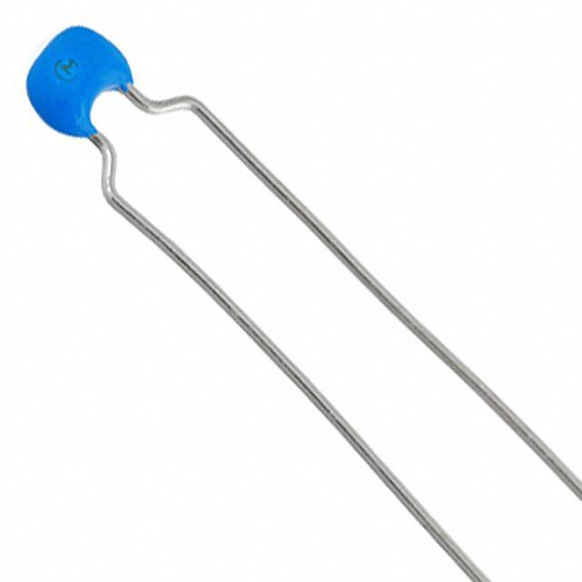


 工商网监
湘ICP备2023018690号
工商网监
湘ICP备2023018690号
