Circuit Components Catalog
Pressure sensor
Built-in amplifier and
compensating circuit
S Package
M Package
New
L Package
P Package
RoHS compliant
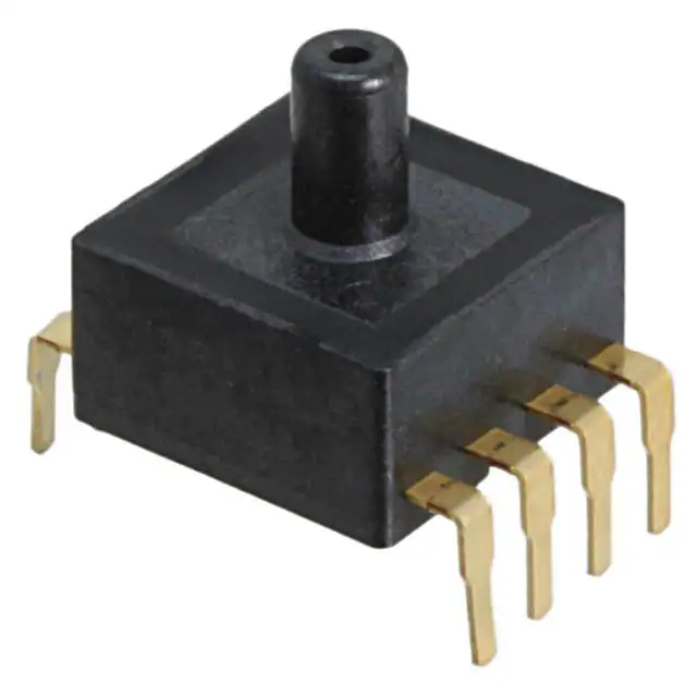
PS-A PRESSURE
SENSOR
FEATURES
TYPICAL APPLICATIONS
1. Contains built-in amplification and
temperature compensation circuit.
Circuit design and adjustment of
characteristics are not required by
users.
2. High-level precision and high
reliability realized.
• Overall accuracy is ±1.25% FS
(Standard type)
• Overall accuracy is ±4% FS
(Economy type)
• Overall accuracy is ±2.5% FS
(Low pressure type)
3. Compact pressure sensor unit that
saves space.
Same size and as previous PS pressure
sensor. (Standard/Economy type, S and
M Packages)
(Please evaluate under actual conditions
before using.)
• Industrial use: pressure switches
and pneumatic devices, etc.
• Medical use: blood pressure
monitors, compressed air pressure
measurement, air beds, etc.
• Other pneumatically operated
pressure devices
Low pressure type
1. Water level detection for household
appliances
Washing machines and dishwashers.
2. Medical applications
Respiratory pressure measuring
instrument, etc.
ORDERING INFORMATION
ADP5 1
1: DIP terminal
0: ±100 kPa
1: –100 kPa
2:
25 kPa
3:
50 kPa
4:
100 kPa
5:
200 kPa
6:
500 kPa
7: 1,000 kPa
A:
40 kPa
B6:
6 kPa (Low pressure type)
0: S Package
length: 3 mm .118 inch, diameter: 3 mm .118 inch
1: M Package
length: 5 mm .197 inch, diameter: 3 mm .118 inch
2: L Package (Only low pressure type)
length: 13.5 mm .531 inch, diameter: 5.45 mm .215 inch
3: P Package (Only low pressure type)
length: 15.6 mm .614 inch, diameter: 5.45 mm .215 inch
Nil: With glass base (Standard type/Low pressure type)
1: Without glass base (Economy type)
Note: Some part numbers may not be available depending on the combination.
Please refer to the Table of PRODUCT TYPES on the next page.
2013.04
industrial.panasonic.com/ac/e/
© Panasonic Corporation 2013
ASCTB244E 201303-T
�PS-A (ADP5)
PRODUCT TYPES
Part No.
Package
(Pressure inlet
hole length)
Pressure
Standard type
S Package
(3mm .118inch)
Economy type
(without glass base)
Low pressure type
Low pressure type
L Package
(13.5mm .531inch)
M Package
(5mm .197inch)
P Package
(15.6mm .614inch)
Terminal
DIP terminal
Standard type
(with glass base)
Standard/Economy type
M Package
(5mm .197inch)
DIP terminal
DIP terminal
DIP terminal
DIP terminal
±100kPa
–100kPa
25kPa
50kPa
100kPa
200kPa
500kPa
1,000kPa
ADP5100
ADP5110
ADP5120
ADP5130
ADP5140
ADP5150
ADP5160
ADP5170
ADP5101
ADP5111
ADP5121
ADP5131
ADP5141
ADP5151
ADP5161
ADP5171
—
—
—
—
—
—
—
—
—
—
—
—
—
—
—
—
—
—
—
—
—
—
—
—
40kPa
—
ADP51A11
—
—
—
6kPa
—
—
ADP51B61
ADP51B62
ADP51B63
Standard packing: Carton: 100 pcs.; Case: 1,000 pcs.
RATING
1. Standard type
Item
Type of pressure
Pressure medium
Rated pressure
Standard type (with glass base)
Gauge pressure
Remarks
Air
±100
Unit: kPa
–100
25
Max. applied pressure
Drive voltage
Temperature compensation range
Offset voltage
Rated output voltage
50
Note*1
100
200
500
Twice the rated pressure
2.5±0.05V
4.5±0.05V
(when
+100kPa)
1,000
1.5 times
the rated
pressure
5±0.25V DC
0 to 50°C 32 to 122°F
0.5±0.05V
Note*2, 3
4.5±0.05V
Note*2, 3
±1.25%FS
Note*3
Note*4
Note*2, 3
Note*2
Note*2, 3
Note*2, 3
Overall accuracy
Current consumption
Output impedance
Source current
Sink current
Max. 10mA
15Ω (Typical)
Max. 0.2mA
Max. 2mA
Notes: 1. Please consult us for pressure media other than air.
2. Indicates output when temperature is 25°C 77°F.
3. Indicates output when drive voltage is 5 V. Although output fluctuates due to fluctuations in the drive voltage, this is not included.
4. Overall accuracy indicates the accuracy of the offset voltage and rated output voltage at a temperature compensation range of 0 to 50°C 32 to 122°F.
2. Economy type
Item
Type of pressure
Pressure medium
Rated pressure
Unit: kPa
Max. applied pressure
Drive voltage
Temperature compensation range
Offset voltage
Span voltage
Offset voltage temperature
characteristics
Sensitivity temperature
characteristics
Current consumption
Output impedance
Source current
Sink current
Economy type (without glass base)
Gauge pressure
Air
40
Twice the rated pressure
3±0.15V DC
5 to 45°C 41 to 113°F
0.3±0.09V
2.4±0.03V
Remarks
±4.0%FS
Note*3, 4
1.3%FS
Note*3, 4
Max. 3mA
20Ω (Typical)
Max. 0.15mA
Max. 1.5mA
Note*2
Note*2, 3
Note*2, 3
Note*2, 3
Note*1
Note*2, 3
Note*2, 3
Notes: 1. Please consult us for pressure media other than air.
2. Indicates output when temperature is 25°C 77°F.
3. Indicates output when drive voltage is 3 V. Although output fluctuates due to fluctuations in the drive voltage, this is not included.
4. Indicates from output value at 25°C 77°F and the change of output at 5 and 45°C 41 to 113°F.
Panasonic Corporation Circuit Components Buisiness Division
industrial.panasonic.com/ac/e/
–2–
© Panasonic Corporation 2013
ASCTB244E 201303-T
�PS-A (ADP5)
3. Low pressure type
Item
Type of pressure
Pressure medium
Rated pressure
Unit: kPa
Max. applied pressure
Drive voltage
Temperature compensation range
Offset voltage
Span voltage
Overall accuracy
Current consumption
Output impedance
Source current
Sink current
Low pressure type
Gauge pressure
Air
6
Twice the rated pressure
5±0.25V DC
0 to 70°C 32 to 158°F
0.5V (Typical)
4.0V (Typical)
±2.5%FS
Max. 10mA
15Ω (Typical)
Max. 0.2mA
Max. 2.0mA
Remarks
Note*1
Note*2
Note*2
Note*2, 3, 4
Notes: 1. Please consult us for pressure media other than air.
2. Indicates output when drive voltage is 5 V. Although output fluctuates due to fluctuations in the drive voltage, this is not included.
3. Overall accuracy indicates the accuracy of the offset voltage and span voltage at temperatures between 0 to 70°C 32 to 158°F (FS=4V)
4. The initial offset voltage error is not included in the overall accuracy.
* Items where no temperature is listed are specifications at 25°C 77°F.
REFERENCE DATA
1. Standard type
1.-(1) Output voltage
1.-(2) Overall accuracy (Offset voltage)
1.-(3) Overall accuracy (Rated output voltage)
ADP5170
Drive voltage: 5V DC
Temperature: 25°C 77°F
Applied pressure: 0 to +1,000kPa
ADP5170
Drive voltage: 5V DC
Temperature: 0 to 50°C 32 to 122°F
Applied pressure: 0kPa
ADP5170
Drive voltage: 5V DC
Temperature: 0 to 50°C 32 to 122°F
Applied pressure: +1,000kPa
Accuracy, %FS
Output voltage, V
4
3
2
1
0
0
500
1.25
1.25
1.00
1.00
0.75
0.75
0.50
0.50
0.25
0.00
-0.25
-0.50
0.25
0.00
-0.25
-0.50
-0.75
-0.75
-1.00
-1.00
-1.25
1000
Accuracy, %FS
5
0
32
Pressure, kPa
25
47
Temperature, °C °F
-1.25
0
32
50
122
25
47
Temperature, °C °F
50
122
2.-(1) Output voltage
2.-(2) Overall accuracy (Offset voltage)
2.-(3) Overall accuracy (Rated output voltage)
ADP5100
Drive voltage: 5V DC
Temperature: 25°C 77°F
Applied pressure: –100 to +100kPa
ADP5100
Drive voltage: 5V DC
Temperature: 0 to 50°C 32 to 122°F
Applied pressure: 0kPa
ADP5100
Drive voltage: 5V DC
Temperature: 0 to 50°C 32 to 122°F
Applied pressure: +100kPa
Accuracy, %FS
Output voltage, V
4
3
2
1.25
1.25
1.00
1.00
0.75
0.75
0.50
0.50
Accuracy, %FS
5
0.25
0.00
-0.50
0
-100
0
Pressure, kPa
100
-0.50
-0.75
-0.75
-1.00
-1.00
-1.25
0
32
25
47
Temperature, °C °F
Panasonic Corporation Circuit Components Buisiness Division
industrial.panasonic.com/ac/e/
0.00
-0.25
-0.25
1
0.25
–3–
50
122
-1.25
0
32
© Panasonic Corporation 2013
25
47
Temperature, °C °F
50
122
ASCTB244E 201303-T
�PS-A (ADP5)
2. Low pressure type
2. THB (high temperature high humidity bias test)
ADP51B61
Drive voltage: 5V
Temperature: 25°C 77°F
Applied pressure: 0 to 6kPa
ADP51B61
Within 85°C 185°F and 85% RH
5 V applied between No. 2 (Vdd) and No. 3 (GND)
Applied pressure: 0kPa
1.00
4.5
4.0
0.80
4.3
3.0
2.0
Span voltage, V
5.0
Offset voltage, V
Output voltage, V
1. Output voltage
0.60
0.40
0.20
1.0
0.0
0.0
3.0
Applied pressure, kPa
3.9
3.7
0.00
6.0
4.1
3.5
intial
100h
500h
intial
100h
500h
4. Shock test
Ambient temperature: 25°C 77°F → 0°C 32°F → 10°C 50°F → 60°C 140°F → 70°C 158°F
ADP51B61
Shock applied: 981 m/s2, 3 times in x, y and z
directions
Applied pressure: 0kPa
4.50
1.00
0.80
4.30
0.80
0.60
0.40
0.20
Offset voltage, V
1.00
Span voltage, V
Offset voltage, V
3. Ambient temperature characteristics
4.10
3.90
25
77
0
10
60
32
50
140
Temperature, °C °F
3.50
70
158
0.40
0.20
3.70
0.00
0.60
0.00
25
77
0
10
60
32
50
140
Temperature, °C °F
70
158
intial
after test
5. Vibration test
1.00
4.50
4.30
0.80
4.30
4.10
3.90
3.70
Span voltage, V
4.50
Offset voltage, V
Span voltage, V
ADP51B61
Vibration applied: 10 to 55 Hz, amplitude: 1.5mm .059inch, x, y and z directions, 2 hrs each
Applied pressure: 0kPa
0.60
0.40
0.20
3.50
after test
3.90
3.70
0.00
intial
4.10
3.50
intial
after test
intial
after test
intial
10cyc
6. Temperature/humidity cycle test
ADP51B61
Exposed to 10 cycles in the temperature and humidity
conditions given below.
Applied pressure: 0kPa
1.00
4.50
0.80
4.30
25°C
77°F
2.5h
3h
2.5h
2.5h
3h
2.5h 1.5h
−10°C
14°F
3.5h
Time
���
95% RH
0% RH
25°C
77°F
3h
Span voltage, V
65°C
149°F
Offset voltage, V
1 cycle (24h)
Temp. 65°C 149°F
0.60
0.40
0.20
3.90
3.70
0.00
3.50
intial
10cyc
Panasonic Corporation Circuit Components Buisiness Division
industrial.panasonic.com/ac/e/
4.10
–4–
© Panasonic Corporation 2013
ASCTB244E 201303-T
�PS-A (ADP5)
3. Evaluation test
Endurance
characteristics
Tested condition
Soldering
resistance
Passed
Passed
Passed
Passed
Temperature/humidity: 40°C 104°F, 90% RH; Operation times: 106, rated voltage applied
Passed
Dropping resistance
Terminal strength
Double amplitude: 1.5 mm .059 inch; Vibration: 10 to 55 Hz;
Applied vibration direction: X, Y, Z 3 directions; Times: 2 hrs each
Dropping height: 75 cm 29.528 inch; Times: 2 times
Pulling strength: 9.8 N {1 kgf}, 10 sec.; Bending strength: 4.9 N {0.5 kgf}, left and right 90° 1 time
Soldered in DIP soldering bath
Temperature (DIP)
Temperature: 230°C 446°F; Time: 5 sec.
Temperature: 260°C 500°F; Time: 10 sec.
Vibration resistance
Mechanical
characteristics
Result
Temperature: Left in a 85°C 185°F constant temperature bath; Time: 100 hrs.
Temperature: Left in a –20°C –4°F constant temperature bath; Time: 100 hrs.
Temperature/humidity: Left at 40°C 104°F, 90% RH; Time: 100 hrs.
Temperature: –20°C to 85°C –4°F to 185°F; 1 cycle: 30 min.; Times of cycle: 100
The CAD data of the products with a CAD Data
DIMENSIONS (mm inch)
1. Standard type S Package (Pressure inlet hole length: 3mm .118inch)
ADP51∗0
CAD Data
mark can be downloaded from: http://industrial.panasonic.com/ac/e/
General tolerance: ±0.3 ±.012
Recommended PC board pattern
6-0.9 dia.
6-.035 dia.
Pressure inlet hole
2.2 dia. .087 dia.
7.0
.276
GND NU NU
7.2
.283
2.5
.098
4-R0.7
4-R.028
1 2 3
Vcc (5V DC) Vout
0.5
.020
2.5
.098
Atmospheric pressure
inlet hole
C
GND
9.5
.374
2.5
.098
6 5 4
0.25
.010
GND NU NU
JAPAN
Terminal No.
1
2
3
4
5
6
7.2
.283
Vcc NU Vout
7.0
.276
2. Standard/Economy type M Package (Pressure inlet hole length: 5mm .197inch)
ADP51∗1/ADP51A11
CAD Data
Name
Vcc (Power supply [+])
NU (Not usable)
Vout (Output)
NU (Not usable)
NU (Not usable)
GND (Ground)
Recommended PC board pattern
Vcc NU Vout
ia.
.9 d ia.
6-0.035 d
6
Pressure inlet hole
2.2 dia. .087 dia.
7.0
.276
GND NU NU
3.0 dia.
.118 dia.
2.5
.098
Terminal connection diagram
R0.2
1.8
R.008 .071
3.0
6.5 .118
.256
Passed
Passed
Passed
Passed
Vcc NU Vout
3.0 dia.
.118 dia.
Passed
7.5
.295
Environmental
characteristics
Tested item
Storage at high temperature
Storage at low temperature
Humidity resistance
Temperature cycle
High temperature/high humidity
operation
7.2
.283
2.5
.098
4-R0.7
4-R.028
R0.2
R.008
5.0
8.5 .197
.335
2.5
.098
7.5
.295
Classification
Terminal connection diagram
1 2 3
Vcc (5V DC) Vout
1.8
.071
C
0.5
.020
2.5
.098
Atmospheric pressure
inlet hole
2.5
.098
0.25
.010
GND NU NU
JAPAN
GND
7.2
.283
Vcc NU Vout
7.0
.276
Panasonic Corporation Circuit Components Buisiness Division
industrial.panasonic.com/ac/e/
6 5 4
9.5
.374
–5–
Terminal No.
1
2
3
4
5
6
© Panasonic Corporation 2013
Name
Vcc (Power supply [+])
NU (Not usable)
Vout (Output)
NU (Not usable)
NU (Not usable)
GND (Ground)
ASCTB244E 201303-T
�PS-A (ADP5)
3. Low pressure type M Package (Pressure inlet hole length: 5mm .197inch)
ADP51B61
General tolerance: ±0.3 ±.012
Recommended PC board pattern
CAD Data
2.54
.100
P2.54×3=7.62
P.100×3=.300
P2.54×3=7.62
P.100×3=.300
8-1.2 dia.
8-.047 dia.
Pressure inlet hole
13.97
.550
10.4
.409
2.54
.100
10.4
.409
Terminal connection diagram
3.0 dia.
.118 dia.
14.0
.551
8 7 6 5
R0.5
R.020
P/N,Lot
1B61
70124
5.0
.197
10.7
.421
JAPAN
0.25
.010
0.76
.030
2.7
.106
1 2 3 4
0.01 µF
1.0 µF
NU Vcc Gnd Vout
Atmospheric pressure inlet hole
Terminal No.
1
2
3
4
5
6
7
8
NU NU NU NU
4. Low pressure type L Package (Pressure inlet hole length: 13.5mm .531inch)
ADP51B62
Name
NU (Not usable)
Vcc (Power supply [+])
GND (Ground)
Vout (Output)
NU (Not usable)
NU (Not usable)
NU (Not usable)
NU (Not usable)
Recommended PC board pattern
CAD Data
2.54
.100
P2.54×3=7.62
P.100×3=.300
P2.54×3=7.62
P.100×3=.300
8-1.2 dia.
8-.047 dia.
Pressure inlet hole
13.97
.550
10.4
.409
2.54
.100
10.4
.409
14.0
.551
R0.5
R.020
C0.3
R.012
8 7 6 5
(13.6)
(.535)
19.3
.760
P/N,Lot
Terminal connection diagram
5.45 dia.
.215 dia.
1B61
70124
JAPAN
1 2 3 4
0.25
.010
0.76
.030
2.7
.106
0.01 µF
1.0 µF
NU Vcc Gnd Vout
Terminal No.
1
2
3
4
5
6
7
8
Atmospheric pressure inlet hole
NU NU NU NU
Panasonic Corporation Circuit Components Buisiness Division
industrial.panasonic.com/ac/e/
–6–
© Panasonic Corporation 2013
Name
NU (Not usable)
Vcc (Power supply [+])
GND (Ground)
Vout (Output)
NU (Not usable)
NU (Not usable)
NU (Not usable)
NU (Not usable)
ASCTB244E 201303-T
�PS-A (ADP5)
5. Low pressure type P Package (Pressure inlet hole length: 15.6mm .614inch)
ADP51B63
General tolerance: ±0.3 ±.012
Recommended PC board pattern
CAD Data
P2.54×3=7.62
P.100×3=.300
2.54
.100
Pressure inlet hole
Atmospheric pressure inlet hole
P2.54×3=7.62
P.100×3=.300
8-1.2 dia.
8-.047 dia.
13.97
.550
10.4
.409
2.54
.100
10.4
.409
Terminal connection diagram
8 7 6 5
14.0
.551
5.45 dia.
.215 dia.
3 dia.
.118 dia.
20.2
.795
P/N, Lot
15.6
.614
5.6
.220
1 2 3 4
1B63
120215
0.01 µF
1.0 µF
JAPAN
0.25
.010
0.76
.030
3.3
.130
Terminal No.
1
2
3
4
5
6
7
8
1 2 3 4
NU Vcc Gnd Vout
NU NU NU NU
8 7 6 5
Panasonic Corporation Circuit Components Buisiness Division
industrial.panasonic.com/ac/e/
–7–
© Panasonic Corporation 2013
Name
NU (Not usable)
Vcc (Power supply [+])
GND (Ground)
Vout (Output)
NU (Not usable)
NU (Not usable)
NU (Not usable)
NU (Not usable)
ASCTB244E 201303-T
�PS-A (ADP5)
NOTES
1. Mounting
Use lands on the printed-circuit boards to
which the sensor can be securely fixed.
2. Soldering
Due to its small size, the thermal capacity
of the pressure sensor DIP type is low.
Therefore, take steps to minimize the
effects of external heat.
Damage and changes to characteristics
may occur due to heat deformation.
Use a non-corrosive resin type of flux.
Since the pressure sensor DIP type is
exposed to the atmosphere, do not allow
flux to enter inside.
1) Manual soldering
• Set the soldering tip from 260 to 300°C
500 to 572°F (30W), and solder for no
more than 5 seconds.
• Please note that output may change if
the pressure is applied on the terminals
when the soldering.
• Thoroughly clean the soldering iron.
2) DIP soldering (DIP terminal type)
• Please keep the DIP solder bath
temperature no higher than 260°C 500°F.
When soldering, heat should be applied
no longer than five seconds.
• When mounting onto a PCB of low
thermal capacity, please avoid DIP
soldering as this may cause heat
deformity.
3) Solder reworking
• Finish reworking in one operation.
• For reworking of the solder bridge, use
a soldering iron with a flat tip. Please do
not add more flux when reworking.
• Please use a soldering iron that is
below the temperature given in the
specifications in order to maintain the
correct temperature at the tip of the
soldering iron.
4) Too much force on the terminals will
cause deformation and loss in
effectiveness of the solder. Therefore,
please avoid dropping and careless
handling of the product.
5) Please control warping of the PCB
within 0.05 mm of the sensor width.
6) When cut folding the PCB after
mounting the sensor, take measures to
prevent stress to the soldered parts.
7) The sensor terminals are designed to
be exposed, so contact of the terminals
with metal shards and the like will cause
output errors. Therefore, please be
careful and prevent things such as metal
shards and hands from contacting the
terminals.
8) To prevent degradation of the PCB
insulation after soldering, please be
careful not to get chemicals on the
sensor when coating.
9) Please consult us regarding the use of
lead-free solder.
3. Connections
1) Please perform connections correctly
in accordance with the terminal
connection diagram. In particular, be
careful not to reverse wire the power
supply as this will cause damage or
degrade to the product.
2) Do not connect terminals that are not
used. This can cause malfunction of the
sensor.
4. Cleaning
1) Since the pressure sensor chip is
exposed to the atmosphere, do not allow
cleaning fluid to enter inside.
2) Avoid ultrasonic cleaning since this
may cause breaks or disconnections in
the wiring.
5. Environment
1) Please avoid using or storing the
pressure sensor chip in a place exposed
to corrosive gases (such as the gases
given off by organic solvents, sulfurous
acid gas, hydrogen sulfides, etc.) which
will adversely affect the performance of
the pressure sensor chip.
2) To ensure resistance to power supply
superimposed noise, you must provide a
capacitor at the power supply input
terminal of the sensor in order to stabilize
the power supply voltage. We
recommend to provide 0.1 µF and 1,000
pF capacitor in parallel. Please confirm
the noise resistance with the actual
equipment and choose adequate
capacitor.
3) Since the internal circuitry may be
destroyed if an external surge voltages is
supplied, provide an element which will
absorb the surges.
4) Malfunctioning may occur if the
product is in the vicinity of electrical noise
such as that from static electricity,
lightning, a broadcasting station, an
amateur radio, or a mobile phone.
5) Since this pressure sensor chip does
not have a water-proof construction,
please do not use the sensor in a location
where it may be sprayed with water, etc.
6) Avoid using the pressure sensors chip
in an environment where condensation
may form.
Furthermore, its output may fluctuate if
any moisture adhering to it freezes.
7) The pressure sensor chip is
constructed in such a way that its output
will fluctuate when it is exposed to light.
Especially when pressure is to be applied
by means of a transparent tube, take
steps to prevent the pressure sensor chip
from being exposed to light.
8) Avoid using the pressure sensor chip
where it will be susceptible to ultrasonic
or other high-frequency vibration.
Panasonic Corporation Circuit Components Buisiness Division
industrial.panasonic.com/ac/e/
–8–
6. Quality check under actual loading
conditions
To assure reliability, check the sensor
under actual loading conditions. Avoid
any situation that may adversely affect its
performance.
7. Other handling precautions
1) That using the wrong pressure range
or mounting method may result in
accidents.
2) The only direct pressure medium you
can use is dry air. The use of other
media, in particular, corrosive gases
(organic solvent based gases, sulfurous
acid based gases, and hydrogen sulfide
based gases, etc.) and media that
contains moisture or foreign substances
will cause malfunction and damage.
Please do not use them.
3) The pressure sensor chip is positioned
inside the pressure inlet hole. Never poke
wires or other foreign matter through the
pressure inlet hole since they may
damage the chip or block the inlet hole.
Avoid use when the atmospheric
pressure inlet is blocked.
4) Use an operating pressure which is
within the rated pressure range. Using a
pressure beyond this range may cause
damage.
5) Since static charge can damage the
pressure sensor chip, bear in mind the
following handling precautions.
(1) When storing the pressure sensor
chips, use a conductive material to short
the pins or wrap the entire chip in
aluminum foil. Plastic containers should
not be used to store or transport the
chips since they readily become charged.
(2) When using the pressure sensor
chips, all the charged articles on the
bench surface and the work personnel
should be grounded so that any ambient
static will be safely discharged.
6) Based on the pressure involved, give
due consideration to the securing of the
pressure sensor DIP type and to the
securing and selection of the inlet tube.
Consult us if you have any queries.
7) When coating a PC board after
mounting the pressure sensor, be sure to
prevent the material from entering the
pressure inlet hole or atmospheric
pressure inlet hole. Use an elastic resin
for coating to avoid expansion and
contraction due to heat, which apply
stress to the sensor.
Please carefully examine the usability.
© Panasonic Corporation 2013
ASCTB244E 201303-T
�