Voltage Regulators
AN79Lxx/AN79LxxM Series
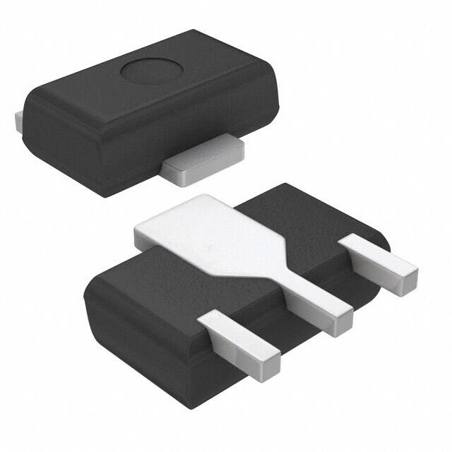
3-pin negative output voltage regulator (100 mA type)
■ Overview
AN79Lxx series
Unit: mm
(1.0)
4.0±0.2
5.1±0.2
5.0±0.2
The AN79Lxx series and the AN79LxxM series are
3-pin, fixed negative output type monolithic voltage
regulators.
Stabilized fixed output voltage is obtained from unstable DC input voltage without using any external components. 12 types of output voltage are available: −4V, −5V,
−6V, −7V, −8V, −9V, −10V, −12V, −15V, −18V, −20V
and −24V. They can be used widely in power circuits with
current capacity of up to 100mA.
(1.0)
2.3±0.2
13.5±0.5
0.6±0.15
0.43+0.1
–0.05
0.43+0.1
–0.05
■ Features
2.54
• No external components
• Output voltage: −4V, −5V, −6V, −7V, −8V, −9V,−10V,
−12V, −15V, −18V, −20V, −24V
• Built-in overcurrent limit circuit
• Built-in thermal overload protection circuit
1 : Output
2 : Common
3 : Intput
2 3 1
SSIP003-P-0000
AN79LxxM series
Unit: mm
1.6 max.
4.6 max.
2.6 max.
1.5
1.5
0.8 min.
0.58 max.
0.48 max.
4.25 max.
2.6 typ.
1.8 max.
0.44 max.
3.0
3
2
1
1 : Common
2 : Input
3 : Output
HSIP003-P-0000B
Note) The packages (SSIP003-P-0000 and HSIP003P-0000B) of this product will be changed to
lead-free type (SSIP003-P-0000S and
2 Common HSIP003-P-0000Q). See the new package di(1)
mensions section later of this datasheet.
■ Block Diagram (AN79Lxx series)
R1
+
Voltage
Reference
Starter
Error Amp.
−
R2
1
Q1
Thermal
Protection
Output
(3)
Pass Tr.
Current
Limiter
RSC
3
Input
(2)
Note) The number in ( ) shows the pin number for the AN79LxxM series.
Publication date: June 2004
SFF00006DEB
1
�AN79Lxx/AN79LxxM Series
■ Absolute Maximum Ratings at Ta = 25°C
Parameter
Symbol
Rating
−35 *1
Input voltage
VI
Power dissipation
PD
−40 *2
650 *3
Operating ambient temperature
Topr
−20 to +80
Storage temperature
AN79Lxx series
V
V
mW
°C
−55 to +150
Tstg
AN79LxxM series
Unit
°C
−55 to +125
*1 AN79L04, AN79L05/M, AN79L06, AN79L07/M, AN79L08/M, AN79L09/M, AN79L10/M, AN79L12/M, AN79L15/M, AN79L18
*2 AN79L20, AN79L24
*3 Follow the derating curve. When Tj exceeds 150°C, the internal circuit cuts off the output.
AN79LxxM series is mounted on a standard board (glass epoxy: 20mm × 20mm × t1.7mm with Cu foil of 1cm2 or more).
■ Electrical Characteristics at Ta = 25°C
• AN79L04 (−4V type)
Parameter
Symbol
Conditions
Output voltage
VO
Tj = 25°C
Output voltage tolerance
VO
VI = −7 to −19V, IO = 1 to 70mA
Line regulation
Load regulation
Bias current
REGIN
REGL
IBias
−4
−3.8
VI = −7 to −17V, Tj = 25°C
Max
−4.16
Unit
V
−4.2
V
80
mV
40
mV
IO = 1 to 100mA, Tj = 25°C
10
60
mV
IO = 1 to 40mA, Tj = 25°C
4.5
30
mV
3
5
mA
0.5
mA
0.1
mA
Tj = 25°C
∆IBias(IN)
VI = −7 to −19V, Tj = 25°C
Bias current fluctuation to load
∆IBias(L)
IO = 1 to 40mA, Tj = 25°C
Ripple rejection ratio
Typ
VI = −6 to −20V, Tj = 25°C
Bias current fluctuation to input
Output noise voltage
Min
−3.84
Vno
f = 10Hz to 100kHz, Ta = 25°C
RR
VI = −7 to −17V, f = 120Hz, Ta = 25°C
38
µV
dB
55
Minimum input/output voltage difference
VDIF(min)
Tj = 25°C
0.8
V
Output short-circuit current
IO(Short)
VI = −35V, Tj = 25°C
200
mA
Output voltage temperature coefficient
∆VO/Ta
IO = 5mA
− 0.4
mV/°C
Note 1) The specified condition Tj = 25°C means that the test should be carried out within so short a test time (within 10ms) that the
characteristic value drift due to the chip junction temperature rise can be ignored.
Note 2) Unless otherwise specified, VI = −9V, IO = 40mA, CI = 2µF, CO = 1µF, Tj = 0 to 125°C
2
SFF00006DEB
�AN79Lxx/AN79LxxM Series
■ Electrical Characteristics at Ta = 25°C (continued)
• AN79L05, AN79L05M (−5V type)
Parameter
Symbol
Conditions
Output voltage
VO
Tj = 25°C
Output voltage tolerance
VO
VI = −8 to −20V, IO = 1 to 70mA
Line regulation
REGIN
Load regulation
REGL
Bias current
IBias
Bias current fluctuation to input
∆IBias(IN)
Bias current fluctuation to load
∆IBias(L)
−4.8
Typ
−5
−4.75
Max
−5.2
Unit
V
−5.25
V
VI = −7 to −21V, Tj = 25°C
100
mV
VI = −8 to −18V, Tj = 25°C
50
mV
IO = 1 to 100mA, Tj = 25°C
11
60
mV
IO = 1 to 40mA, Tj = 25°C
5
30
mV
Tj = 25°C
3
5
mA
0.5
mA
0.1
mA
VI = −8 to −20V, Tj = 25°C
IO = 1 to 40mA, Tj = 25°C
Output noise voltage
Vno
f = 10Hz to 100kHz, Ta = 25°C
Ripple rejection ratio
RR
VI = −8 to −18V, f = 120Hz, Ta = 25°C
VDIF(min)
Tj = 25°C
Output short-circuit current
IO(Short)
VI = −35V, Tj = 25°C
Output voltage temperature coefficient
∆VO/Ta
IO = 5mA
Minimum input/output voltage difference
Min
µV
40
dB
55
0.8
V
200
mA
− 0.4
mV/°C
Note 1) The specified condition Tj = 25°C means that the test should be carried out within so short a test time (within 10ms) that the
characteristic value drift due to the chip junction temperature rise can be ignored.
Note 2) Unless otherwise specified, VI = −10V, IO = 40mA, CI = 2µF, CO = 1µF, Tj = 0 to 125°C (AN79L05) and Tj = 0 to 100°C
(AN79L05M)
• AN79L06 (−6V type)
Parameter
Symbol
Conditions
Output voltage
VO
Tj = 25°C
Output voltage tolerance
VO
VI = −9 to −21V, IO = 1 to 70mA
Line regulation
REGIN
Load regulation
REGL
Bias current
IBias
Min
−5.76
Typ
−6
−5.7
Max
−6.24
Unit
V
−6.3
V
VI = −8 to −22V, Tj = 25°C
120
mV
VI = −9 to −19V, Tj = 25°C
60
mV
IO = 1 to 100mA, Tj = 25°C
12
60
mV
IO = 1 to 40mA, Tj = 25°C
5.5
30
mV
3
5
mA
Tj = 25°C
Bias current fluctuation to input
∆IBias(IN)
VI = −9 to −21V, Tj = 25°C
0.5
mA
Bias current fluctuation to load
∆IBias(L)
IO = 1 to 40mA, Tj = 25°C
0.1
mA
Output noise voltage
Ripple rejection ratio
Vno
f = 10Hz to 100kHz, Ta = 25°C
RR
VI = −9 to −19V, f = 120Hz, Ta = 25°C
VDIF(min)
Tj = 25°C
Output short-circuit current
IO(Short)
VI = −35V, Tj = 25°C
Output voltage temperature coefficient
∆VO/Ta
IO = 5mA
Minimum input/output voltage difference
44
55
µV
dB
0.8
V
200
mA
− 0.4
mV/°C
Note 1) The specified condition Tj = 25°C means that the test should be carried out within so short a test time (within 10ms) that the
characteristic value drift due to the chip junction temperature rise can be ignored.
Note 2) Unless otherwise specified, VI = −11V, IO = 40mA, CI = 2µF, CO = 1µF, Tj = 0 to 125°C
SFF00006DEB
3
�AN79Lxx/AN79LxxM Series
■ Electrical Characteristics at Ta = 25°C (continued)
• AN79L07, AN79L07M (−7V type)
Parameter
Symbol
Conditions
Min
Output voltage
VO
Tj = 25°C
−6.72
Output voltage tolerance
VO
VI = −10 to −22V, IO = 1 to 70mA
−6.65
Line regulation
Load regulation
Bias current
REGIN
REGL
IBias
Typ
−7
VI = −9 to −23V, Tj = 25°C
VI = −10 to −20V, Tj = 25°C
Max
−7.28
Unit
V
−7.35
V
140
mV
70
mV
IO = 1 to 100mA, Tj = 25°C
13
70
mV
IO = 1 to 40mA, Tj = 25°C
6
40
mV
Tj = 25°C
3
5
mA
Bias current fluctuation to input
∆IBias(IN)
VI = −10 to −22V, Tj = 25°C
0.5
mA
Bias current fluctuation to load
∆IBias(L)
IO = 1 to 40mA, Tj = 25°C
0.1
mA
Output noise voltage
Vno
f = 10Hz to 100kHz, Ta = 25°C
Ripple rejection ratio
RR
VI = −10 to −20V, f = 120Hz, Ta = 25°C
µV
48
dB
54
Minimum input/output voltage difference
VDIF(min)
Tj = 25°C
0.8
V
Output short-circuit current
IO(Short)
VI = −35V, Tj = 25°C
200
mA
Output voltage temperature coefficient
∆VO/Ta
IO = 5mA
− 0.5
mV/°C
Note 1) The specified condition Tj = 25°C means that the test should be carried out within so short a test time (within 10ms) that the
characteristic value drift due to the chip junction temperature rise can be ignored.
Note 2) Unless otherwise specified, VI = −12V, IO = 40mA, CI = 2µF, CO = 1µF, Tj = 0 to 125°C (AN79L07) and Tj = 0 to 100°C
(AN79L07M)
• AN79L08, AN79L08M (−8V type)
Parameter
Symbol
Conditions
Output voltage
VO
Tj = 25°C
Output voltage tolerance
VO
VI = −11 to −23V, IO = 1 to 70mA
Line regulation
Load regulation
Bias current
REGIN
REGL
IBias
Min
−7.68
Typ
−8
−7.6
VI = −10 to −24V, Tj = 25°C
VI = −11 to −21V, Tj = 25°C
Max
−8.32
Unit
V
−8.4
V
160
mV
80
mV
IO = 1 to 100mA, Tj = 25°C
15
80
mV
IO = 1 to 40mA, Tj = 25°C
7
40
mV
Tj = 25°C
3
5
mA
Bias current fluctuation to input
∆IBias(IN)
VI = −11 to −23V, Tj = 25°C
0.5
mA
Bias current fluctuation to load
∆IBias(L)
IO = 1 to 40mA, Tj = 25°C
0.1
mA
Output noise voltage
Vno
f = 10Hz to 100kHz, Ta = 25°C
Ripple rejection ratio
RR
VI = −11 to −21V, f = 120Hz, Ta = 25°C
52
µV
dB
54
Minimum input/output voltage difference
VDIF(min)
Tj = 25°C
0.8
V
Output short-circuit current
IO(Short)
VI = −35V, Tj = 25°C
200
mA
Output voltage temperature coefficient
∆VO/Ta
IO = 5mA, Tj = 0 to 125°C
− 0.6
mV/°C
Note 1) The specified condition Tj = 25°C means that the test should be carried out within so short a test time (within 10ms) that the
characteristic value drift due to the chip junction temperature rise can be ignored.
Note 2) Unless otherwise specified, VI = −14V, IO = 40mA, CI = 2µF, CO = 1µF, Tj = 0 to 125°C (AN79L08) and Tj = 0 to 100°C
(AN79L08M)
4
SFF00006DEB
�AN79Lxx/AN79LxxM Series
■ Electrical Characteristics at Ta = 25°C (continued)
• AN79L09, AN79L09M (−9V type)
Parameter
Symbol
Conditions
Min
Output voltage
VO
Tj = 25°C
−8.64
Output voltage tolerance
VO
VI = −12 to −24V, IO = 1 to 70mA
−8.55
Line regulation
REGIN
Load regulation
REGL
Bias current
IBias
Bias current fluctuation to input
∆IBias(IN)
Bias current fluctuation to load
∆IBias(L)
−9
Max
−9.36
Unit
V
−9.45
V
VI = −11 to −25V, Tj = 25°C
160
mV
VI = −12 to −22V, Tj = 25°C
80
mV
IO = 1 to 100mA, Tj = 25°C
16
90
mV
IO = 1 to 40mA, Tj = 25°C
8
50
mV
Tj = 25°C
3
5
mA
0.5
mA
0.1
mA
VI = −12 to −24V, Tj = 25°C
IO = 1 to 40mA, Tj = 25°C
Output noise voltage
Vno
f = 10Hz to 100kHz, Ta = 25°C
Ripple rejection ratio
RR
VI = −12 to −22V, f = 120Hz, Ta = 25°C
VDIF(min)
Tj = 25°C
Output short-circuit current
IO(Short)
VI = −35V, Tj = 25°C
Output voltage temperature coefficient
∆VO/Ta
IO = 5mA, Tj = 0 to 125°C
Minimum input/output voltage difference
Typ
µV
58
dB
53
0.8
V
200
mA
− 0.6
mV/°C
Note 1) The specified condition Tj = 25°C means that the test should be carried out within so short a test time (within 10ms) that the
characteristic value drift due to the chip junction temperature rise can be ignored.
Note 2) Unless otherwise specified, VI = −15V, IO = 40mA, CI = 2µF, CO = 1µF, Tj = 0 to 125°C (AN79L09) and Tj = 0 to 100°C
(AN79L09M)
• AN79L10, AN79L10M (−10V type)
Parameter
Symbol
Conditions
Min
Output voltage
VO
Tj = 25°C
−9.6
Output voltage tolerance
VO
VI = −13 to −25V, IO = 1 to 70mA
−9.5
Line regulation
Load regulation
Bias current
REGIN
REGL
Typ
−10
VI = −12 to −26V, Tj = 25°C
VI = −13 to −23V, Tj = 25°C
Max
−10.4
Unit
V
−10.5
V
160
mV
80
mV
IO = 1 to 100mA, Tj = 25°C
17
100
mV
IO = 1 to 40mA, Tj = 25°C
9
50
mV
Tj = 25°C
3
5
mA
Bias current fluctuation to input
∆IBias(IN)
VI = −13 to −25V, Tj = 25°C
0.5
mA
Bias current fluctuation to load
∆IBias(L)
IO = 1 to 40mA, Tj = 25°C
0.1
mA
Output noise voltage
Ripple rejection ratio
IBias
Vno
f = 10Hz to 100kHz, Ta = 25°C
RR
VI = −13 to −23V, f = 120Hz, Ta = 25°C
65
µV
dB
53
Minimum input/output voltage difference
VDIF(min)
Tj = 25°C
0.8
V
Output short-circuit current
IO(Short)
VI = −35V, Tj = 25°C
200
mA
Output voltage temperature coefficient
∆VO/Ta
IO = 5mA
− 0.7
mV/°C
Note 1) The specified condition Tj = 25°C means that the test should be carried out within so short a test time (within 10ms) that the
characteristic value drift due to the chip junction temperature rise can be ignored.
Note 2) Unless otherwise specified, VI = −16V, IO = 40mA, CI = 2µF, CO = 1µF, Tj = 0 to 125°C (AN79L10) and Tj = 0 to 100°C
(AN79L10M)
SFF00006DEB
5
�AN79Lxx/AN79LxxM Series
■ Electrical Characteristics at Ta = 25°C (continued)
• AN79L12, AN79L12M (−12V type)
Parameter
Symbol
Conditions
Min
Output voltage
VO
Tj = 25°C
−11.5
Output voltage tolerance
VO
VI = −15 to −27V, IO = 1 to 70mA
−11.4
Line regulation
REGIN
Load regulation
REGL
Bias current
IBias
Bias current fluctuation to input
∆IBias(IN)
Bias current fluctuation to load
∆IBias(L)
−12
Max
−12.5
Unit
V
−12.6
V
VI = −14.5 to −30V, Tj = 25°C
200
mV
VI = −15 to −25V, Tj = 25°C
100
mV
IO = 1 to 100mA, Tj = 25°C
20
100
mV
IO = 1 to 40mA, Tj = 25°C
10
50
mV
3
5
mA
0.5
mA
0.1
mA
Tj = 25°C
VI = −15 to −27V, Tj = 25°C
IO = 1 to 40mA, Tj = 25°C
Output noise voltage
Vno
f = 10Hz to 100kHz, Ta = 25°C
Ripple rejection ratio
RR
VI = −15 to −25V, f = 120Hz, Ta = 25°C
VDIF(min)
Tj = 25°C
Output short-circuit current
IO(Short)
VI = −35V, Tj = 25°C
Output voltage temperature coefficient
∆VO/Ta
IO = 5mA
Minimum input/output voltage difference
Typ
µV
75
dB
52
0.8
V
200
mA
− 0.8
mV/°C
Note 1) The specified condition Tj = 25°C means that the test should be carried out within so short a test time (within 10ms) that the
characteristic value drift due to the chip junction temperature rise can be ignored.
Note 2) Unless otherwise specified, VI = −19V, IO = 40mA, CI = 2µF, CO = 1µF, Tj = 0 to 125°C (AN79L12) and Tj = 0 to 100°C
(AN79L12M)
• AN79L15, AN79L15M (−15V type)
Parameter
Symbol
Conditions
Output voltage
VO
Tj = 25°C
Output voltage tolerance
VO
VI = −18 to −28V, IO = 1 to 70mA
Line regulation
Load regulation
Bias current
REGIN
REGL
IBias
Min
−14.4
Typ
−15
−14.25
VI = −17.5 to −33V, Tj = 25°C
VI = −18 to −28V, Tj = 25°C
Max
−15.6
Unit
V
−15.75
V
200
mV
100
mV
IO = 1 to 100mA, Tj = 25°C
25
130
mV
IO = 1 to 40mA, Tj = 25°C
12
60
mV
3
5
mA
Tj = 25°C
Bias current fluctuation to input
∆IBias(IN)
VI = −18 to −30V, Tj = 25°C
0.5
mA
Bias current fluctuation to load
∆IBias(L)
IO = 1 to 40mA, Tj = 25°C
0.1
mA
Output noise voltage
Vno
f = 10Hz to 100kHz, Ta = 25°C
Ripple rejection ratio
RR
VI = −18 to −28V, f = 120Hz, Ta = 25°C
90
µV
dB
51
Minimum input/output voltage difference
VDIF(min)
Tj = 25°C
0.8
V
Output short-circuit current
IO(Short)
VI = −35V, Tj = 25°C
200
mA
Output voltage temperature coefficient
∆VO/Ta
IO = 5mA
− 0.9
mV/°C
Note 1) The specified condition Tj = 25°C means that the test should be carried out within so short a test time (within 10ms) that the
characteristic value drift due to the chip junction temperature rise can be ignored.
Note 2) Unless otherwise specified, VI = −23V, IO = 40mA, CI = 2µF, CO = 1µF, Tj = 0 to 125°C (AN79L15) and Tj = 0 to 100°C
(AN79L15M)
6
SFF00006DEB
�AN79Lxx/AN79LxxM Series
■ Electrical Characteristics at Ta = 25°C (continued)
• AN79L18 (−18V type)
Parameter
Symbol
Conditions
Min
Output voltage
VO
Tj = 25°C
−17.3
Output voltage tolerance
VO
VI = −21 to −33V, IO = 1 to 70mA
−17.1
Line regulation
Load regulation
Bias current
REGIN
REGL
IBias
Typ
−18
Max
Unit
−18.7
V
−18.9
V
VI = −21 to −33V, Tj = 25°C
200
mV
VI = −21 to −32V, Tj = 25°C
100
mV
IO = 1 to 100mA, Tj = 25°C
30
160
mV
IO = 1 to 40mA, Tj = 25°C
15
80
mV
3
5
mA
0.5
mA
0.1
mA
Tj = 25°C
Bias current fluctuation to input
∆IBias(IN)
VI = −21 to −33V, Tj = 25°C
Bias current fluctuation to load
∆IBias(L)
IO = 1 to 40mA, Tj = 25°C
Output noise voltage
Vno
f = 10Hz to 100kHz, Ta = 25°C
Ripple rejection ratio
RR
VI = −22 to −32V, f = 120Hz, Ta = 25°C
µV
110
50
dB
Minimum input/output voltage difference
VDIF(min)
Tj = 25°C
0.8
V
Output short-circuit current
IO(Short)
VI = −35V, Tj = 25°C
200
mA
Output voltage temperature coefficient
∆VO/Ta
IO = 5mA
−1
mV/°C
Note 1) The specified condition Tj = 25°C means that the test should be carried out within so short a test time (within 10ms) that the
characteristic value drift due to the chip junction temperature rise can be ignored.
Note 2) Unless otherwise specified, VI = −27V, IO = 40mA, CI = 2µF, CO = 1µF, Tj = 0 to 125°C
• AN79L20 (−20V type)
Parameter
Symbol
Conditions
Output voltage
VO
Tj = 25°C
Output voltage tolerance
VO
VI = −23 to −35V, IO = 1 to 70mA
Line regulation
REGIN
Load regulation
REGL
Bias current
IBias
Min
−19.2
Typ
−20
−19
Max
−20.8
Unit
V
−21
V
VI = −23 to −35V, Tj = 25°C
200
mV
VI = −24 to −34V, Tj = 25°C
100
mV
IO = 1 to 100mA, Tj = 25°C
35
180
mV
IO = 1 to 40mA, Tj = 25°C
17
90
mV
3
5
mA
Tj = 25°C
Bias current fluctuation to input
∆IBias(IN)
VI = −23 to −35V, Tj = 25°C
0.5
mA
Bias current fluctuation to load
∆IBias(L)
IO = 1 to 40mA, Tj = 25°C
0.1
mA
Output noise voltage
Ripple rejection ratio
Vno
f = 10Hz to 100kHz, Ta = 25°C
RR
VI = −24 to −34V, f = 120Hz, Ta = 25°C
135
49
µV
dB
Minimum input/output voltage difference
VDIF(min)
Tj = 25°C
0.8
V
Output short-circuit current
IO(Short)
VI = −35V, Tj = 25°C
200
mA
Output voltage temperature coefficient
∆VO/Ta
IO = 5mA
−1
mV/°C
Note 1) The specified condition Tj = 25°C means that the test should be carried out within so short a test time (within 10ms) that the
characteristic value drift due to the chip junction temperature rise can be ignored.
Note 2) Unless otherwise specified, VI = −29V, IO = 40mA, CI = 2µF, CO = 1µF, Tj = 0 to 125°C
SFF00006DEB
7
�AN79Lxx/AN79LxxM Series
■ Electrical Characteristics at Ta = 25°C (continued)
• AN79L24 (−24V type)
Parameter
Symbol
Conditions
Min
Output voltage
VO
Tj = 25°C
Output voltage tolerance
VO
VI = −27 to −38V, IO = 1 to 70mA
Line regulation
REGIN
Load regulation
REGL
Bias current
Typ
−23
−25
V
−25.2
V
VI = −27 to −38V, Tj = 25°C
200
mV
VI = −27 to −37V, Tj = 25°C
100
mV
−22.8
IO = 1 to 100mA, Tj = 25°C
40
200
mV
IO = 1 to 40mA, Tj = 25°C
20
100
mV
3
5
mA
0.5
mA
0.1
mA
Tj = 25°C
IBias
Unit
Max
−24
Bias current fluctuation to input
∆IBias(IN)
VI = −27 to −38V, Tj = 25°C
Bias current fluctuation to load
∆IBias(L)
IO = 1 to 40mA, Tj = 25°C
Output noise voltage
Vno
f = 10Hz to 100kHz, Ta = 25°C
Ripple rejection ratio
RR
VI = −28 to −38V, f = 120Hz, Ta = 25°C
µV
170
49
dB
Minimum input/output voltage difference
VDIF(min)
Tj = 25°C
0.8
V
Output short-circuit current
IO(Short)
VI = −35V, Tj = 25°C
200
mA
Output voltage temperature coefficient
∆VO/Ta
IO = 5mA
−1
mV/°C
Note 1) The specified condition Tj = 25°C means that the test should be carried out within so short a test time (within 10ms) that the
characteristic value drift due to the chip junction temperature rise can be ignored.
Note 2) Unless otherwise specified, VI = −33V, IO = 40mA, CI = 2µF, CO = 1µF, Tj = 0 to 125°C
■ Main Characteristics
PD Ta (AN79Lxx series)
PD Ta (AN79LxxM series)
VO T j
−5.12
1.0
0.8
0.6
0.4
0.2
Mounted on standard board
(glass epoxy: 20 mm × 20 mm × t1.7mm
with Cu foil of 1cm2 or more)
AN79L05
VI = −10V
IO = 1mA
−5.08
0.8
Output voltage VO (V)
Independent IC
without a heat sink
Rth(j-a) = 190°C/W
PD = 658mW (25°C)
Power dissipation PD (W)
Power dissipation PD (W)
1.0
0.6
0.4
0.2
−5.04
−5.00
−4.96
−4.92
−4.88
−4.84
0
0
0
20
40
60
80 100 120 140 160
Ambient temperature Ta (°C)
8
0
20
40
60
80 100 120 140 160
Ambient temperature Ta (°C)
SFF00006DEB
−4.80
−25
0
25
50
75
100
Junction temperature Tj (°C)
125
�AN79Lxx/AN79LxxM Series
Load transient response
20
AN79L05
AN79L05
15
1.2
IO = 100mA
1.0
IO
=2
0m
IO
=1 A
IO = 0mA
1m
A
0.8
0.6
0.4
−50
0
50
100
150
10
5
10
0
−10
−20
0
2
4
Junction temperature Tj (°C)
6
Time t (µs)
8
10
Input voltage VI (V)
Output voltage fluctuation (V)
Input transient response
AN79L05
200
100
0
1
0
−1
−2
0
10
20
30
40
50
Time t (µs)
RR f
Ripple rejection ratio RR (dB)
120
AN79L05
IO = 5mA
100
80
60
40
20
0
10
100
1k
10k
100k
Frequency f (Hz)
■ Basic Regulator Circuit
−VI Input
Output
−VO
1
3
AN79Lxx
CI
−
+
2
−
Common +
CO
Connect CI of 2µF when the input line is long.
CO improves the transient response. 1µF
SFF00006DEB
9
Load current IO (mA)
VDIF(min) Tj
1.4
Output voltage fluctuation (mV)
Minimum input/output voltage difference VDIF(min) (V)
■ Main Characteristics (continued)
�AN79Lxx/AN79LxxM Series
■ Usage Notes
1. Cautions for a basic circuit
CI: When a wiring from a smoothing circuit to a three-pin regulator
is long, it is likely to oscillate at output. A capacitor of 0.1µF to
0.47µF should be connected near an input pin.
CO: Deadly needed to prevent from oscillation (0.33µF to 1.0µF). It
is recommended to use a capacitor of a small internal impedance (ex. tantalum capacitor) when using it under a low temperature.
When any sudden change of load current is likely to occur, connect an electrolytic capacitor of 10µF to 100µF to improve a
transitional response of output voltage.
Di: Normally unnecessary. But add it in the case that there is a
residual voltage at the output capacitor Co even after switching
off the supply power because a current is likely to flow into an
output pin of the IC and damage the IC.
Di
VI
VO
3
1
CI
CO
2
Figure 1
2. Other caution items
1) Short-circuit between the input pin and GND pin
If the input pin is short-circuitted to GND or is cut
off when a large capacitance capacitor has been connected to the IC's load, a voltage of a capacitor connected to an output pin is applied between input/output of the IC and this likely results in damage of the
IC. It is necessary, therefore, to connect a diode, as
shown in figure 2, to counter the reverse bias between
input/output pins.
In
3
1
2
GND
Output
Out
−
+
CO
Figure 2
2) Floating of GND pin
If a GND pin is made floating in an operating mode, an unstabilized input voltage is outputted. In this case, a
thermal protection circuit inside the IC does not normally operate. In this state, if the load is short-circuited or
overloaded, it is likely to damage the IC.
■ Application Circuit Example
−VI Input
3
1
−VO
Output
AN79Lxx
2
−
+
VO'
R2
Common
−
2µF
+
IBias
1µF
R1
R
|VO | = VO' 1 + R1 + IQR1
2
Note) VO varies due to sample to sample variation of IBias .
Never fail to adjust individually with R1 .
10
SFF00006DEB
�AN79Lxx/AN79LxxM Series
■ New Package Dimensions (Unit: mm)
• SSIP003-P-0000S (Lead-free package)
4.00±0.20
(1.00)
(1.00)
5.00±0.20
5.00±0.20
0.60±0.15
1
1.27
2.30±0.20
0.40+0.10
-0.05
13.30±0.50
0.40±0.10
3
1.27
• HSIP003-P-0000Q (Lead-free package)
1.00+0.10
-0.20
2.50±0.10
1
0.40+0.10
-0.05
1.50
3
0.40+0.10
-0.05
0.50+0.10
-0.05
0.15 M
0.42+0.10
-0.05
(0.75)
1.50±0.10
3.00
2.65±0.10
0.10
(0.40)
4.00+0.25
-0.20
4.50±0.10
1.55±0.20
SFF00006DEB
11
�Request for your special attention and precautions in using the technical information
and semiconductors described in this material
(1) An export permit needs to be obtained from the competent authorities of the Japanese Government if any of
the products or technical information described in this material and controlled under the "Foreign Exchange
and Foreign Trade Law" is to be exported or taken out of Japan.
(2) The technical information described in this material is limited to showing representative characteristics and
applied circuits examples of the products. It neither warrants non-infringement of intellectual property right
or any other rights owned by our company or a third party, nor grants any license.
(3) We are not liable for the infringement of rights owned by a third party arising out of the use of the technical
information as described in this material.
(4) The products described in this material are intended to be used for standard applications or general electronic equipment (such as office equipment, communications equipment, measuring instruments and household appliances).
Consult our sales staff in advance for information on the following applications:
• Special applications (such as for airplanes, aerospace, automobiles, traffic control equipment, combustion equipment, life support systems and safety devices) in which exceptional quality and reliability are
required, or if the failure or malfunction of the products may directly jeopardize life or harm the human
body.
• Any applications other than the standard applications intended.
(5) The products and product specifications described in this material are subject to change without notice for
modification and/or improvement. At the final stage of your design, purchasing, or use of the products,
therefore, ask for the most up-to-date Product Standards in advance to make sure that the latest specifications satisfy your requirements.
(6) When designing your equipment, comply with the guaranteed values, in particular those of maximum rating, the range of operating power supply voltage, and heat radiation characteristics. Otherwise, we will not
be liable for any defect which may arise later in your equipment.
Even when the products are used within the guaranteed values, take into the consideration of incidence of
break down and failure mode, possible to occur to semiconductor products. Measures on the systems such
as redundant design, arresting the spread of fire or preventing glitch are recommended in order to prevent
physical injury, fire, social damages, for example, by using the products.
(7) When using products for which damp-proof packing is required, observe the conditions (including shelf life
and amount of time let standing of unsealed items) agreed upon when specification sheets are individually
exchanged.
(8) This material may be not reprinted or reproduced whether wholly or partially, without the prior written
permission of Matsushita Electric Industrial Co., Ltd.
2003 SEP
�