Voltage Regulators
AN80LxxRMS Series
Positive output, low dropout voltage regulator (150 mA type)
■ Overview
Unit: mm
The AN80LxxRMS series is a 0.15 A, low dropout,
positive voltage regulator with reset function. 20 classifications of output voltages, 1.8 V, 1.9 V, 2.0 V, 2.1 V, 2.2
V, 2.5 V, 2.8 V, 2.9 V, 3.0 V, 3.1 V, 3.2 V, 3.3 V, 3.4 V, 3.5
V, 3.6 V, 4.8 V, 4.9 V, 5.0 V, 5.1 V and 5.2 V are available.
In addition, it is adopting the surface mounting type package, so that it is most suited for miniaturization and weight
reduction of set equipment.
+0.20
2.80 –0.30
1.50 +0.25
–0.05
3
1
2
0.16 –0.06
0 to 0.10
• Minimum input and output voltage difference: 0.4 V
max.
• High accuracy output voltage: (allowance: ±3%)
• Built-in reset function terminal (high: active)
• Built-in overcurrent limit circuit
• Built-in rush current prevention circuit at input voltage rise
• Output voltage: 1.8 V to 5.2 V
0.80
1.10 –0.10
+0.20
■ Features
+0.10
0.30 –0.05
+0.10
0.95
1.90±0.10
4
0.95
2.90 –0.05
+0.20
5
0.65±0.15
1.45±0.10
0.65±0.15
0.1 to 0.30
0.40±0.20
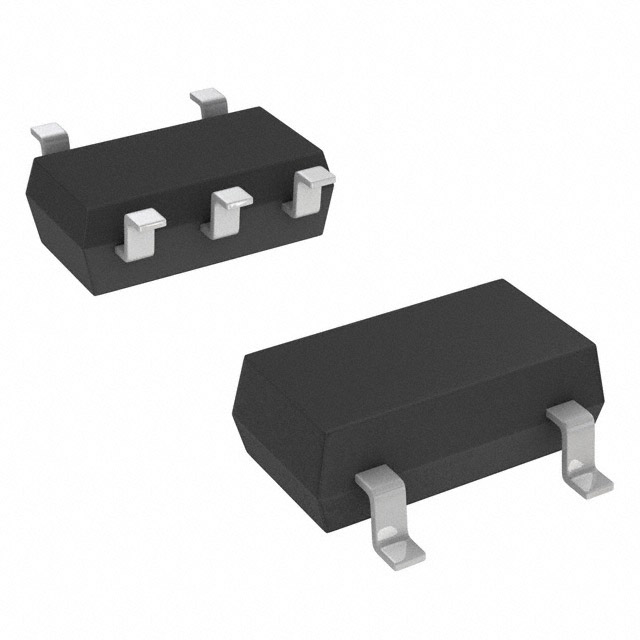
MINI-5D
On marking, see page 2
■ Applications
• Cellular phone, PHS, analog cordless phone, other
small sized portable equipment
■ Block Diagram
IN 1
2
OUT
3
N.C.
Current
source
CONT 5
Start/Stop
Error
amp.
Bandgap
reference
4
GND
Publication date: February 2002
SFF00008DEB
1
�AN80LxxRMS Series
■ Output Voltage Characteristics at IOUT = 50 mA, Ta = 25°C
Type No.
Output V
AN80L18RMS
1.8
AN80L19RMS
1.9
AN80L20RMS
Conditions
Min
Type
Max
Unit
Marking
1.746
1.8
1.854
V
BA
2.9
1.843
1.9
1.957
V
BB
2.0
3.0
1.940
2.0
2.060
V
BC
AN80L21RMS
2.1
3.1
2.037
2.1
2.163
V
BD
AN80L22RMS
2.2
3.2
2.134
2.2
2.266
V
BE
AN80L25RMS
2.5
3.5
2.425
2.5
2.575
V
BW
AN80L28RMS
2.8
3.8
2.716
2.8
2.884
V
BF
AN80L29RMS
2.9
3.9
2.813
2.9
2.987
V
BG
AN80L30RMS
3.0
4.0
2.910
3.0
3.090
V
BH
AN80L31RMS
3.1
4.1
3.007
3.1
3.193
V
BJ
AN80L32RMS
3.2
4.2
3.104
3.2
3.296
V
BK
AN80L33RMS
3.3
4.3
3.201
3.3
3.399
V
BL
AN80L34RMS
3.4
4.4
3.298
3.4
3.502
V
BM
AN80L35RMS
3.5
4.5
3.395
3.5
3.605
V
BN
AN80L36RMS
3.6
4.6
3.492
3.6
3.708
V
BP
AN80L48RMS
4.8
5.8
4.656
4.8
4.944
V
BQ
AN80L49RMS
4.9
5.9
4.753
4.9
5.047
V
BR
AN80L50RMS
5.0
6.0
4.850
5.0
5.150
V
BS
AN80L51RMS
5.1
6.1
4.947
5.1
5.253
V
BT
AN80L52RMS
5.2
6.2
5.044
5.2
5.356
V
BU
VIN = 2.8 V
BA
(Marking example: AN80L18RMS)
■ Pin Descriptions
Pin No.
Description
1
Input voltage pin
2
Output voltage pin
3
N.C. pin
4
Grounding pin
5
Control pin
(High → operation, Low → stop)
2
SFF00008DEB
�AN80LxxRMS Series
■ Absolute Maximum Ratings
Parameter
Symbol
Rating
Unit
Supply voltage *1
VCC
14.6
V
Supply current
ICC
300
mA
Power dissipation *3
PD
78
mW
Operating ambient temperature *2
Topr
−30 to +85
°C
Storage temperature *2
Tstg
−55 to +150
°C
Note) *1: There may be a case of the device destruction when the output (VOUT) and the grounding (GND), or the output (VOUT) and
input (VIN) are short-circuited.
2:
Except
for the operating ambient temperature and storage temperature, all ratings are for Ta = 25°C.
*
3:
T
=
Power
dissipation for IC alone without heat sink at +85°C.
*
opr
■ Recommended Operating Conditions
Part No.
Output voltage
Operating supply voltage range (VCC)
Unit
AN80L18RMS
1.8
2.2 to 14.5
V
AN80L19RMS
1.9
2.3 to 14.5
V
AN80L20RMS
2.0
2.4 to 14.5
V
AN80L21RMS
2.1
2.5 to 14.5
V
AN80L22RMS
2.2
2.6 to 14.5
V
AN80L25RMS
2.5
2.9 to 14.5
V
AN80L28RMS
2.8
3.2 to 14.5
V
AN80L29RMS
2.9
3.3 to 14.5
V
AN80L30RMS
3.0
3.4 to 14.5
V
AN80L31RMS
3.1
3.5 to 14.5
V
AN80L32RMS
3.2
3.6 to 14.5
V
AN80L33RMS
3.3
3.7 to 14.5
V
AN80L34RMS
3.4
3.8 to 14.5
V
AN80L35RMS
3.5
3.9 to 14.5
V
AN80L36RMS
3.6
4.0 to 14.5
V
AN80L48RMS
4.8
5.2 to 14.5
V
AN80L49RMS
4.9
5.3 to 14.5
V
AN80L50RMS
5.0
5.4 to 14.5
V
AN80L51RMS
5.1
5.5 to 14.5
V
AN80L52RMS
5.2
5.6 to 14.5
V
SFF00008DEB
3
�AN80LxxRMS Series
■ Electrical Characteristics at Ta = 25°C
• AN80L18RMS (1.8 V type)
Unless otherwise specially provided, shorten each test time (within 10 ms) so that the test is conducted under the condition
that the drift due to the temperature increase in the chip junction part can be neglected. CIN = 0.1 µF, COUT = 10 µF
Parameter
Symbol
Min
Typ
Max
Unit
VIN = 2.8 V, IOUT = 50 mA
1.746
1.8
1.854
V
Line regulation 1
REGIN1 VIN = 2.8 V → 14.5 V, IOUT = 50 mA
10
50
mV
Line regulation 2
REGIN2 VIN = 2.8 V → 9 V, IOUT = 50 mA
5
20
mV
REGLOA VIN = 2.8 V, IOUT = 0 mA → 150 mA
50
150
mV
IPEAK
VIN = 2.8 V, The output current value
when VOUT decreases by 5% from its
value at IOUT = 50 mA.
180
240
mA
IBIAS
VIN = 2.8 V, IOUT = 0 mA
350
µA
VIN = 2.8 V, IOUT = 0 mA → 150 mA
5
mA
Output voltage
Load regulation
VOUT
*1
Peak output current
*2
Bias current under no load
Conditions
Bias current fluctuation to load
∆IBIAS
Standby consumption current
ISTB
VIN = 10 V, VCONT = 0 V
0.1
µA
Bias current before starting
regulation
IRUSH
VIN = 1.5 V, IOUT = 0 mA
1.5
5
mA
1 V[rms], f = 120 Hz, IOUT = 10 mA
62
70
dB
Ripple rejection ratio
RR
Minimum input/
output voltage difference 1
VDIF(min)1 VIN = 1.5 V, IOUT = 0 mA
0.1
0.2
V
Minimum input/
output voltage difference 2
VDIF(min)2 VIN = 2.1 V, IOUT = 150 mA
0.4
V
Control terminal threshold high voltage VCONTH VIN = 2.8 V, IOUT = 50 mA
1.50
V
Control terminal threshold low voltage VCONTL VIN = 2.8 V, IOUT = 50 mA
0.30
V
30
µA
Control terminal current
ICONT
VIN = 2.8 V, IOUT = 50 mA
VCONT = 1.8 V
Note) *1: 1.0 Ω
*2: Peak output current: The output current when the output voltage has been decreased by 5% from the value at the time
when the output current is 50 mA due to the overcurrent protection.
• Design reference data
Note) The following values are typical and not guaranteed values.
Parameter
Symbol
Conditions
Typ
Max
Unit
10 Hz ≤ f ≤ 100 kHz, IOUT = 10 mA
38
µV
1
dVOUT
Output voltage tempera·
ture coefficient
VOUT
dT
VIN = 2.8 V, IOUT = 0 mA
−30°C ≤ Ta ≤ +85°C
90
ppm/°C
Output rise time *
VIN = 2.8 V, IOUT = 50 mA
VCONT = 0 V → 1.8 V, CIN = 0.1 µF
COUT = 10 µF, VOUT = 90%
0.10
ms
Output noise voltage
VNO
tON
Note) *: Refer to "■ Application Notes 3. Output rise-time characteristics".
4
Min
SFF00008DEB
�AN80LxxRMS Series
■ Electrical Characteristics at Ta = 25°C (continued)
• AN80L19RMS (1.9 V type)
Unless otherwise specially provided, shorten each test time (within 10 ms) so that the test is conducted under the condition
that the drift due to the temperature increase in the chip junction part can be neglected. CIN = 0.1 µF, COUT = 10 µF
Parameter
Symbol
Min
Typ
Max
Unit
VIN = 2.9 V, IOUT = 50 mA
1.843
1.9
1.957
V
Line regulation 1
REGIN1 VIN = 2.9 V → 14.5 V, IOUT = 50 mA
10
50
mV
Line regulation 2
REGIN2 VIN = 2.9 V → 9 V, IOUT = 50 mA
5
20
mV
REGLOA VIN = 2.9 V, IOUT = 0 mA → 150 mA
50
150
mV
IPEAK
VIN = 2.9 V, The output current value
when VOUT decreases by 5% from its
value at IOUT = 50 mA.
180
240
mA
IBIAS
VIN = 2.9 V, IOUT = 0 mA
350
µA
VIN = 2.9 V, IOUT = 0 mA → 150 mA
5
mA
Output voltage
Load regulation
VOUT
*1
Peak output current
*2
Bias current under no load
Conditions
Bias current fluctuation to load
∆IBIAS
Standby consumption current
ISTB
VIN = 10 V, VCONT = 0 V
0.1
µA
Bias current before starting
regulation
IRUSH
VIN = 1.6 V, IOUT = 0 mA
1.5
5
mA
1 V[rms], f = 120 Hz, IOUT = 10 mA
62
70
dB
Ripple rejection ratio
RR
Minimum input/
output voltage difference 1
VDIF(min)1 VIN = 1.6 V, IOUT = 0 mA
0.1
0.2
V
Minimum input/
output voltage difference 2
VDIF(min)2 VIN = 2.2 V, IOUT = 150 mA
0.4
V
Control terminal threshold high voltage VCONTH VIN = 2.9 V, IOUT = 50 mA
1.50
V
Control terminal threshold low voltage VCONTL VIN = 2.9 V, IOUT = 50 mA
0.30
V
30
µA
Control terminal current
ICONT
VIN = 2.9 V, IOUT = 50 mA
VCONT = 1.8 V
Note) *1: 1.0 Ω
*2: Peak output current: The output current when the output voltage has been decreased by 5% from the value at the time
when the output current is 50 mA due to the overcurrent protection.
• Design reference data
Note) The following values are typical and not guaranteed values.
Parameter
Symbol
Conditions
Min
Typ
Max
Unit
10 Hz ≤ f ≤ 100 kHz, IOUT = 10 mA
40
µV
1
dVOUT
Output voltage tempera·
ture coefficient
VOUT
dT
VIN = 2.9 V, IOUT = 0 mA
−30°C ≤ Ta ≤ +85°C
90
ppm/°C
Output rise time *
VIN = 2.9 V, IOUT = 50 mA
VCONT = 0 V → 1.8 V, CIN = 0.1 µF
COUT = 10 µF, VOUT = 90%
0.10
ms
Output noise voltage
VNO
tON
Note) *: Refer to "■ Application Notes 3. Output rise-time characteristics".
SFF00008DEB
5
�AN80LxxRMS Series
■ Electrical Characteristics at Ta = 25°C (continued)
• AN80L20RMS (2.0 V type)
Unless otherwise specially provided, shorten each test time (within 10 ms) so that the test is conducted under the condition
that the drift due to the temperature increase in the chip junction part can be neglected. CIN = 0.1 µF, COUT = 10 µF
Parameter
Symbol
Min
Typ
Max
Unit
VIN = 3.0 V, IOUT = 50 mA
1.940
2.0
2.060
V
Line regulation 1
REGIN1 VIN = 3.0 V → 14.5 V, IOUT = 50 mA
10
50
mV
Line regulation 2
REGIN2 VIN = 3.0 V → 9 V, IOUT = 50 mA
5
20
mV
REGLOA VIN = 3.0 V, IOUT = 0 mA → 150 mA
50
150
mV
IPEAK
VIN = 3.0 V, The output current value
when VOUT decreases by 5% from its
value at IOUT = 50 mA.
180
240
mA
IBIAS
VIN = 3.0 V, IOUT = 0 mA
350
µA
VIN = 3.0 V, IOUT = 0 mA → 150 mA
5
mA
Output voltage
Load regulation
VOUT
*1
Peak output current
*2
Bias current under no load
Conditions
Bias current fluctuation to load
∆IBIAS
Standby consumption current
ISTB
VIN = 10 V, VCONT = 0 V
0.1
µA
Bias current before starting
regulation
IRUSH
VIN = 1.7 V, IOUT = 0 mA
1.5
5
mA
1 V[rms], f = 120 Hz, IOUT = 10 mA
62
70
dB
Ripple rejection ratio
RR
Minimum input/
output voltage difference 1
VDIF(min)1 VIN = 1.7 V, IOUT = 0 mA
0.1
0.2
V
Minimum input/
output voltage difference 2
VDIF(min)2 VIN = 2.3 V, IOUT = 150 mA
0.4
V
Control terminal threshold high voltage VCONTH VIN = 3.0 V, IOUT = 50 mA
1.50
V
Control terminal threshold low voltage VCONTL VIN = 3.0 V, IOUT = 50 mA
0.30
V
30
µA
Control terminal current
ICONT
VIN = 3.0 V, IOUT = 50 mA
VCONT = 1.8 V
Note) *1: 1.0 Ω
*2: Peak output current: The output current when the output voltage has been decreased by 5% from the value at the time
when the output current is 50 mA due to the overcurrent protection.
• Design reference data
Note) The following values are typical and not guaranteed values.
Parameter
Symbol
Conditions
Typ
Max
Unit
10 Hz ≤ f ≤ 100 kHz, IOUT = 10 mA
42
µV
1
dVOUT
Output voltage tempera·
ture coefficient
VOUT
dT
VIN = 3.0 V, IOUT = 0 mA
−30°C ≤ Ta ≤ +85°C
90
ppm/°C
Output rise time *
VIN = 3.0 V, IOUT = 50 mA
VCONT = 0 V → 1.8 V, CIN = 0.1 µF
COUT = 10 µF, VOUT = 90%
0.10
ms
Output noise voltage
VNO
tON
Note) *: Refer to "■ Application Notes 3. Output rise-time characteristics".
6
Min
SFF00008DEB
�AN80LxxRMS Series
■ Electrical Characteristics at Ta = 25°C (continued)
• AN80L21RMS (2.1 V type)
Unless otherwise specially provided, shorten each test time (within 10 ms) so that the test is conducted under the condition
that the drift due to the temperature increase in the chip junction part can be neglected. CIN = 0.1 µF, COUT = 10 µF
Parameter
Symbol
Min
Typ
Max
Unit
VIN = 3.1 V, IOUT = 50 mA
2.037
2.1
2.163
V
Line regulation 1
REGIN1 VIN = 3.1 V → 14.5 V, IOUT = 50 mA
10
50
mV
Line regulation 2
REGIN2 VIN = 3.1 V → 9 V, IOUT = 50 mA
5
20
mV
REGLOA VIN = 3.1 V, IOUT = 0 mA → 150 mA
50
150
mV
IPEAK
VIN = 3.1 V, The output current value
when VOUT decreases by 5% from its
value at IOUT = 50 mA.
180
240
mA
IBIAS
VIN = 3.1 V, IOUT = 0 mA
350
µA
VIN = 3.1 V, IOUT = 0 mA → 150 mA
5
mA
Output voltage
Load regulation
VOUT
*1
Peak output current
*2
Bias current under no load
Conditions
Bias current fluctuation to load
∆IBIAS
Standby consumption current
ISTB
VIN = 10 V, VCONT = 0 V
0.1
µA
Bias current before starting
regulation
IRUSH
VIN = 1.8 V, IOUT = 0 mA
1.5
5
mA
1 V[rms], f = 120 Hz, IOUT = 10 mA
61
69
dB
Ripple rejection ratio
RR
Minimum input/
output voltage difference 1
VDIF(min)1 VIN = 1.8 V, IOUT = 0 mA
0.1
0.2
V
Minimum input/
output voltage difference 2
VDIF(min)2 VIN = 2.4 V, IOUT = 150 mA
0.4
V
Control terminal threshold high voltage VCONTH VIN = 3.1 V, IOUT = 50 mA
1.50
V
Control terminal threshold low voltage VCONTL VIN = 3.1 V, IOUT = 50 mA
0.30
V
30
µA
Control terminal current
ICONT
VIN = 3.1 V, IOUT = 50 mA
VCONT = 1.8 V
Note) *1: 1.0 Ω
*2: Peak output current: The output current when the output voltage has been decreased by 5% from the value at the time
when the output current is 50 mA due to the overcurrent protection.
• Design reference data
Note) The following values are typical and not guaranteed values.
Parameter
Symbol
Conditions
Min
Typ
Max
Unit
10 Hz ≤ f ≤ 100 kHz, IOUT = 10 mA
44
µV
1
dVOUT
Output voltage tempera·
ture coefficient
VOUT
dT
VIN = 3.1 V, IOUT = 0 mA
−30°C ≤ Ta ≤ +85°C
90
ppm/°C
Output rise time *
VIN = 3.1 V, IOUT = 50 mA
VCONT = 0 V → 1.8 V, CIN = 0.1 µF
COUT = 10 µF, VOUT = 90%
0.10
ms
Output noise voltage
VNO
tON
Note) *: Refer to "■ Application Notes 3. Output rise-time characteristics".
SFF00008DEB
7
�AN80LxxRMS Series
■ Electrical Characteristics at Ta = 25°C (continued)
• AN80L22RMS (2.2 V type)
Unless otherwise specially provided, shorten each test time (within 10 ms) so that the test is conducted under the condition
that the drift due to the temperature increase in the chip junction part can be neglected. CIN = 0.1 µF, COUT = 10 µF
Parameter
Symbol
Min
Typ
Max
Unit
VIN = 3.2 V, IOUT = 50 mA
2.134
2.2
2.266
V
Line regulation 1
REGIN1 VIN = 3.2 V → 14.5 V, IOUT = 50 mA
10
50
mV
Line regulation 2
REGIN2 VIN = 3.2 V → 9 V, IOUT = 50 mA
5
20
mV
REGLOA VIN = 3.2 V, IOUT = 0 mA → 150 mA
50
150
mV
IPEAK
VIN = 3.2 V, The output current value
when VOUT decreases by 5% from its
value at IOUT = 50 mA.
180
240
mA
IBIAS
VIN = 3.2 V, IOUT = 0 mA
350
µA
VIN = 3.2 V, IOUT = 0 mA → 150 mA
5
mA
Output voltage
Load regulation
VOUT
*1
Peak output current
*2
Bias current under no load
Conditions
Bias current fluctuation to load
∆IBIAS
Standby consumption current
ISTB
VIN = 10 V, VCONT = 0 V
0.1
µA
Bias current before starting
regulation
IRUSH
VIN = 1.9 V, IOUT = 0 mA
1.5
5
mA
1 V[rms], f = 120 Hz, IOUT = 10 mA
61
69
dB
Ripple rejection ratio
RR
Minimum input/
output voltage difference 1
VDIF(min)1 VIN = 1.9 V, IOUT = 0 mA
0.1
0.2
V
Minimum input/
output voltage difference 2
VDIF(min)2 VIN = 2.4 V, IOUT = 150 mA
0.4
V
Control terminal threshold high voltage VCONTH VIN = 3.2 V, IOUT = 50 mA
1.50
V
Control terminal threshold low voltage VCONTL VIN = 3.2 V, IOUT = 50 mA
0.30
V
30
µA
Control terminal current
ICONT
VIN = 3.2 V, IOUT = 50 mA
VCONT = 1.8 V
Note) *1: 1.0 Ω
*2: Peak output current: The output current when the output voltage has been decreased by 5% from the value at the time
when the output current is 50 mA due to the overcurrent protection.
• Design reference data
Note) The following values are typical and not guaranteed values.
Parameter
Symbol
Conditions
Typ
Max
Unit
10 Hz ≤ f ≤ 100 kHz, IOUT = 10 mA
46
µV
1
dVOUT
Output voltage tempera·
ture coefficient
VOUT
dT
VIN = 3.2 V, IOUT = 0 mA
−30°C ≤ Ta ≤ +85°C
90
ppm/°C
Output rise time *
VIN = 3.2 V, IOUT = 50 mA
VCONT = 0 V → 1.8 V, CIN = 0.1 µF
COUT = 10 µF, VOUT = 90%
0.10
ms
Output noise voltage
VNO
tON
Note) *: Refer to "■ Application Notes 3. Output rise-time characteristics".
8
Min
SFF00008DEB
�AN80LxxRMS Series
■ Electrical Characteristics at Ta = 25°C (continued)
• AN80L25RMS (2.5 V type)
Unless otherwise specially provided, shorten each test time (within 10 ms) so that the test is conducted under the condition
that the drift due to the temperature increase in the chip junction part can be neglected. CIN = 0.1 µF, COUT = 10 µF
Parameter
Symbol
Min
Typ
Max
Unit
VIN = 3.5 V, IOUT = 50 mA
2.425
2.5
2.575
V
Line regulation 1
REGIN1 VIN = 3.5 V → 14.5 V, IOUT = 50 mA
10
50
mV
Line regulation 2
REGIN2 VIN = 3.5 V → 9 V, IOUT = 50 mA
5
20
mV
REGLOA VIN = 3.5 V, IOUT = 0 mA → 150 mA
50
150
mV
IPEAK
VIN = 3.5 V, The output current value
when VOUT decreases by 5% from its
value at IOUT = 50 mA.
180
240
mA
IBIAS
VIN = 3.5 V, IOUT = 0 mA
350
µA
VIN = 3.5 V, IOUT = 0 mA → 150 mA
5
mA
Output voltage
Load regulation
VOUT
*1
Peak output current
*2
Bias current under no load
Conditions
Bias current fluctuation to load
∆IBIAS
Standby consumption current
ISTB
VIN = 10 V, VCONT = 0 V
0.1
µA
Bias current before starting
regulation
IRUSH
VIN = 2.2 V, IOUT = 0 mA
1.5
5
mA
1 V[rms], f = 120 Hz, IOUT = 10 mA
60
68
dB
Ripple rejection ratio
RR
Minimum input/
output voltage difference 1
VDIF(min)1 VIN = 2.2 V, IOUT = 0 mA
0.1
0.2
V
Minimum input/
output voltage difference 2
VDIF(min)2 VIN = 2.6 V, IOUT = 150 mA
0.4
V
Control terminal threshold high voltage VCONTH VIN = 3.5 V, IOUT = 50 mA
1.50
V
Control terminal threshold low voltage VCONTL VIN = 3.5 V, IOUT = 50 mA
0.30
V
30
µA
Control terminal current
ICONT
VIN = 3.5 V, IOUT = 50 mA
VCONT = 1.8 V
Note) *1: 1.0 Ω
*2: Peak output current: The output current when the output voltage has been decreased by 5% from the value at the time
when the output current is 50 mA due to the overcurrent protection.
• Design reference data
Note) The following values are typical and not guaranteed values.
Parameter
Symbol
Conditions
Min
Typ
Max
Unit
10 Hz ≤ f ≤ 100 kHz, IOUT = 10 mA
58
µV
1
dVOUT
Output voltage tempera·
ture coefficient
VOUT
dT
VIN = 3.5 V, IOUT = 0 mA
−30°C ≤ Ta ≤ +85°C
90
ppm/°C
Output rise time *
VIN = 3.15 V, IOUT = 50 mA
VCONT = 0 V → 1.8 V, CIN = 0.1 µF
COUT = 10 µF, VOUT = 90%
0.10
ms
Output noise voltage
VNO
tON
Note) *: Refer to "■ Application Notes 3. Output rise-time characteristics".
SFF00008DEB
9
�AN80LxxRMS Series
■ Electrical Characteristics at Ta = 25°C (continued)
• AN80L28RMS (2.8 V type)
Unless otherwise specially provided, shorten each test time (within 10 ms) so that the test is conducted under the condition
that the drift due to the temperature increase in the chip junction part can be neglected. CIN = 0.1 µF, COUT = 10 µF
Parameter
Symbol
Min
Typ
Max
Unit
VIN = 3.8 V, IOUT = 50 mA
2.716
2.8
2.884
V
Line regulation 1
REGIN1 VIN = 3.8 V → 14.5 V, IOUT = 50 mA
10
50
mV
Line regulation 2
REGIN2 VIN = 3.8 V → 9 V, IOUT = 50 mA
5
20
mV
REGLOA VIN = 3.8 V, IOUT = 0 mA → 150 mA
50
150
mV
IPEAK
VIN = 3.8 V, The output current value
when VOUT decreases by 5% from its
value at IOUT = 50 mA.
180
240
mA
IBIAS
VIN = 3.8 V, IOUT = 0 mA
350
µA
VIN = 3.8 V, IOUT = 0 mA → 150 mA
5
mA
Output voltage
Load regulation
VOUT
*1
Peak output current
*2
Bias current under no load
Conditions
Bias current fluctuation to load
∆IBIAS
Standby consumption current
ISTB
VIN = 10 V, VCONT = 0 V
0.1
µA
Bias current before starting
regulation
IRUSH
VIN = 2.5 V, IOUT = 0 mA
1.5
5
mA
1 V[rms], f = 120 Hz, IOUT = 10 mA
60
68
dB
Ripple rejection ratio
RR
Minimum input/
output voltage difference 1
VDIF(min)1 VIN = 2.5 V, IOUT = 0 mA
0.1
0.2
V
Minimum input/
output voltage difference 2
VDIF(min)2 VIN = 2.9 V, IOUT = 150 mA
0.4
V
Control terminal threshold high voltage VCONTH VIN = 3.8 V, IOUT = 50 mA
1.50
V
Control terminal threshold low voltage VCONTL VIN = 3.8 V, IOUT = 50 mA
0.30
V
30
µA
Control terminal current
ICONT
VIN = 3.8 V, IOUT = 50 mA
VCONT = 1.8 V
Note) *1: 1.0 Ω
*2: Peak output current: The output current when the output voltage has been decreased by 5% from the value at the time
when the output current is 50 mA due to the overcurrent protection.
• Design reference data
Note) The following values are typical and not guaranteed values.
Parameter
Symbol
Conditions
Min
Typ
Max
Unit
10 Hz ≤ f ≤ 100 kHz, IOUT = 10 mA
58
µV
1
dVOUT
Output voltage tempera·
ture coefficient
VOUT
dT
VIN = 3.8 V, IOUT = 0 mA
−30°C ≤ Ta ≤ +85°C
90
ppm/°C
Output rise time *
VIN = 3.8 V, IOUT = 50 mA
VCONT = 0 V → 1.8 V, CIN = 0.1 µF
COUT = 10 µF, VOUT = 90%
0.10
ms
Output noise voltage
VNO
tON
Note) *: Refer to "■ Application Notes 3. Output rise-time characteristics".
10
SFF00008DEB
�AN80LxxRMS Series
■ Electrical Characteristics at Ta = 25°C (continued)
• AN80L29RMS (2.9 V type)
Unless otherwise specially provided, shorten each test time (within 10 ms) so that the test is conducted under the condition
that the drift due to the temperature increase in the chip junction part can be neglected. CIN = 0.1 µF, COUT = 10 µF
Parameter
Symbol
Min
Typ
Max
Unit
VIN = 3.9 V, IOUT = 50 mA
2.813
2.9
2.987
V
Line regulation 1
REGIN1 VIN = 3.9 V → 14.5 V, IOUT = 50 mA
10
50
mV
Line regulation 2
REGIN2 VIN = 3.9 V → 9 V, IOUT = 50 mA
5
20
mV
REGLOA VIN = 3.9 V, IOUT = 0 mA → 150 mA
50
150
mV
IPEAK
VIN = 3.9 V, The output current value
when VOUT decreases by 5% from its
value at IOUT = 50 mA.
180
240
mA
IBIAS
VIN = 3.9 V, IOUT = 0 mA
350
µA
VIN = 3.9 V, IOUT = 0 mA → 150 mA
5
mA
Output voltage
Load regulation
VOUT
*1
Peak output current
*2
Bias current under no load
Conditions
Bias current fluctuation to load
∆IBIAS
Standby consumption current
ISTB
VIN = 10 V, VCONT = 0 V
0.1
µA
Bias current before starting
regulation
IRUSH
VIN = 2.6 V, IOUT = 0 mA
1.5
5
mA
1 V[rms], f = 120 Hz, IOUT = 10 mA
60
68
dB
Ripple rejection ratio
RR
Minimum input/
output voltage difference 1
VDIF(min)1 VIN = 2.6 V, IOUT = 0 mA
0.1
0.2
V
Minimum input/
output voltage difference 2
VDIF(min)2 VIN = 3.0 V, IOUT = 150 mA
0.4
V
Control terminal threshold high voltage VCONTH VIN = 3.9 V, IOUT = 50 mA
1.50
V
Control terminal threshold low voltage VCONTL VIN = 3.9 V, IOUT = 50 mA
0.30
V
30
µA
Control terminal current
ICONT
VIN = 3.9 V, IOUT = 50 mA
VCONT = 1.8 V
Note) *1: 1.0 Ω
*2: Peak output current: The output current when the output voltage has been decreased by 5% from the value at the time
when the output current is 50 mA due to the overcurrent protection.
• Design reference data
Note) The following values are typical and not guaranteed values.
Parameter
Symbol
Conditions
Min
Typ
Max
Unit
10 Hz ≤ f ≤ 100 kHz, IOUT = 10 mA
60
µV
1
dVOUT
Output voltage tempera·
ture coefficient
VOUT
dT
VIN = 3.9 V, IOUT = 0 mA
−30°C ≤ Ta ≤ +85°C
90
ppm/°C
Output rise time *
VIN = 3.9 V, IOUT = 50 mA
VCONT = 0 V → 1.8 V, CIN = 0.1 µF
COUT = 10 µF, VOUT = 90%
0.12
ms
Output noise voltage
VNO
tON
Note) *: Refer to "■ Application Notes 3. Output rise-time characteristics".
SFF00008DEB
11
�AN80LxxRMS Series
■ Electrical Characteristics at Ta = 25°C (continued)
• AN80L30RMS (3.0 V type)
Unless otherwise specially provided, shorten each test time (within 10 ms) so that the test is conducted under the condition
that the drift due to the temperature increase in the chip junction part can be neglected. CIN = 0.1 µF, COUT = 10 µF
Parameter
Symbol
Min
Typ
Max
Unit
VIN = 4.0 V, IOUT = 50 mA
2.910
3.0
3.090
V
Line regulation 1
REGIN1 VIN = 4.0 V → 14.5 V, IOUT = 50 mA
10
50
mV
Line regulation 2
REGIN2 VIN = 4.0 V → 9 V, IOUT = 50 mA
5
20
mV
REGLOA VIN = 4.0 V, IOUT = 0 mA → 150 mA
50
150
mV
IPEAK
VIN = 4.0 V, The output current value
when VOUT decreases by 5% from its
value at IOUT = 50 mA.
180
240
mA
IBIAS
VIN = 4.0 V, IOUT = 0 mA
350
µA
VIN = 4.0 V, IOUT = 0 mA → 150 mA
5
mA
Output voltage
Load regulation
VOUT
*1
Peak output current
*2
Bias current under no load
Conditions
Bias current fluctuation to load
∆IBIAS
Standby consumption current
ISTB
VIN = 10 V, VCONT = 0 V
0.1
µA
Bias current before starting
regulation
IRUSH
VIN = 2.7 V, IOUT = 0 mA
1.5
5
mA
1 V[rms], f = 120 Hz, IOUT = 10 mA
60
68
dB
Ripple rejection ratio
RR
Minimum input/
output voltage difference 1
VDIF(min)1 VIN = 2.7 V, IOUT = 0 mA
0.1
0.2
V
Minimum input/
output voltage difference 2
VDIF(min)2 VIN = 3.1 V, IOUT = 150 mA
0.4
V
Control terminal threshold high voltage VCONTH VIN = 4.0 V, IOUT = 50 mA
1.50
V
Control terminal threshold low voltage VCONTL VIN = 4.0 V, IOUT = 50 mA
0.30
V
30
µA
Control terminal current
ICONT
VIN = 4.0 V, IOUT = 50 mA
VCONT = 1.8 V
Note) *1: 1.0 Ω
*2: Peak output current: The output current when the output voltage has been decreased by 5% from the value at the time
when the output current is 50 mA due to the overcurrent protection.
• Design reference data
Note) The following values are typical and not guaranteed values.
Parameter
Symbol
Conditions
Min
Typ
Max
Unit
10 Hz ≤ f ≤ 100 kHz, IOUT = 10 mA
62
µV
1
dVOUT
Output voltage tempera·
ture coefficient
VOUT
dT
VIN = 4.0 V, IOUT = 0 mA
−30°C ≤ Ta ≤ +85°C
90
ppm/°C
Output rise time *
VIN = 4.0 V, IOUT = 50 mA
VCONT = 0 V → 1.8 V, CIN = 0.1 µF
COUT = 10 µF, VOUT = 90%
0.12
ms
Output noise voltage
VNO
tON
Note) *: Refer to "■ Application Notes 3. Output rise-time characteristics".
12
SFF00008DEB
�AN80LxxRMS Series
■ Electrical Characteristics at Ta = 25°C (continued)
• AN80L31RMS (3.1 V type)
Unless otherwise specially provided, shorten each test time (within 10 ms) so that the test is conducted under the condition
that the drift due to the temperature increase in the chip junction part can be neglected. CIN = 0.1 µF, COUT = 10 µF
Parameter
Symbol
Min
Typ
Max
Unit
VIN = 4.1 V, IOUT = 50 mA
3.007
3.1
3.193
V
Line regulation 1
REGIN1 VIN = 4.1 V → 14.5 V, IOUT = 50 mA
10
50
mV
Line regulation 2
REGIN2 VIN = 4.1 V → 9 V, IOUT = 50 mA
5
20
mV
REGLOA VIN = 4.1 V, IOUT = 0 mA → 150 mA
50
150
mV
IPEAK
VIN = 4.1 V, The output current value
when VOUT decreases by 5% from its
value at IOUT = 50 mA.
180
240
mA
IBIAS
VIN = 4.1 V, IOUT = 0 mA
350
µA
VIN = 4.1 V, IOUT = 0 mA → 150 mA
5
mA
Output voltage
Load regulation
VOUT
*1
Peak output current
*2
Bias current under no load
Conditions
Bias current fluctuation to load
∆IBIAS
Standby consumption current
ISTB
VIN = 10 V, VCONT = 0 V
0.1
µA
Bias current before starting
regulation
IRUSH
VIN = 2.8 V, IOUT = 0 mA
1.5
5
mA
1 V[rms], f = 120 Hz, IOUT = 10 mA
59
67
dB
Ripple rejection ratio
RR
Minimum input/
output voltage difference 1
VDIF(min)1 VIN = 2.8 V, IOUT = 0 mA
0.1
0.2
V
Minimum input/
output voltage difference 2
VDIF(min)2 VIN = 3.2 V, IOUT = 150 mA
0.4
V
Control terminal threshold high voltage VCONTH VIN = 4.1 V, IOUT = 50 mA
1.50
V
Control terminal threshold low voltage VCONTL VIN = 4.1 V, IOUT = 50 mA
0.30
V
30
µA
Control terminal current
ICONT
VIN = 4.1 V, IOUT = 50 mA
VCONT = 1.8 V
Note) *1: 1.0 Ω
*2: Peak output current: The output current when the output voltage has been decreased by 5% from the value at the time
when the output current is 50 mA due to the overcurrent protection.
• Design reference data
Note) The following values are typical and not guaranteed values.
Parameter
Symbol
Conditions
Min
Typ
Max
Unit
10 Hz ≤ f ≤ 100 kHz, IOUT = 10 mA
64
µV
1
dVOUT
Output voltage tempera·
ture coefficient
VOUT
dT
VIN = 4.1 V, IOUT = 0 mA
−30°C ≤ Ta ≤ +85°C
90
ppm/°C
Output rise time *
VIN = 4.1 V, IOUT = 50 mA
VCONT = 0 V → 1.8 V, CIN = 0.1 µF
COUT = 10 µF, VOUT = 90%
0.12
ms
Output noise voltage
VNO
tON
Note) *: Refer to "■ Application Notes 3. Output rise-time characteristics".
SFF00008DEB
13
�AN80LxxRMS Series
■ Electrical Characteristics at Ta = 25°C (continued)
• AN80L32RMS (3.2 V type)
Unless otherwise specially provided, shorten each test time (within 10 ms) so that the test is conducted under the condition
that the drift due to the temperature increase in the chip junction part can be neglected. CIN = 0.1 µF, COUT = 10 µF
Parameter
Symbol
Min
Typ
Max
Unit
VIN = 4.2 V, IOUT = 50 mA
3.104
3.2
3.296
V
Line regulation 1
REGIN1 VIN = 4.2 V → 14.5 V, IOUT = 50 mA
10
50
mV
Line regulation 2
REGIN2 VIN = 4.2 V → 9 V, IOUT = 50 mA
5
20
mV
REGLOA VIN = 4.2 V, IOUT = 0 mA → 150 mA
50
150
mV
IPEAK
VIN = 4.2 V, The output current value
when VOUT decreases by 5% from its
value at IOUT = 50 mA.
180
240
mA
IBIAS
VIN = 4.2 V, IOUT = 0 mA
350
µA
VIN = 4.2 V, IOUT = 0 mA → 150 mA
5
mA
Output voltage
Load regulation
VOUT
*1
Peak output current
*2
Bias current under no load
Conditions
Bias current fluctuation to load
∆IBIAS
Standby consumption current
ISTB
VIN = 10 V, VCONT = 0 V
0.1
µA
Bias current before starting
regulation
IRUSH
VIN = 2.9 V, IOUT = 0 mA
1.5
5
mA
1 V[rms], f = 120 Hz, IOUT = 10 mA
59
67
dB
Ripple rejection ratio
RR
Minimum input/
output voltage difference 1
VDIF(min)1 VIN = 2.9 V, IOUT = 0 mA
0.1
0.2
V
Minimum input/
output voltage difference 2
VDIF(min)2 VIN = 3.3 V, IOUT = 150 mA
0.4
V
Control terminal threshold high voltage VCONTH VIN = 4.2 V, IOUT = 50 mA
1.50
V
Control terminal threshold low voltage VCONTL VIN = 4.2 V, IOUT = 50 mA
0.30
V
30
µA
Control terminal current
ICONT
VIN = 4.2 V, IOUT = 50 mA
VCONT = 1.8 V
Note) *1: 1.0 Ω
*2: Peak output current: The output current when the output voltage has been decreased by 5% from the value at the time
when the output current is 50 mA due to the overcurrent protection.
• Design reference data
Note) The following values are typical and not guaranteed values.
Parameter
Symbol
Conditions
Min
Typ
Max
Unit
10 Hz ≤ f ≤ 100 kHz, IOUT = 10 mA
66
µV
1
dVOUT
Output voltage tempera·
ture coefficient
VOUT
dT
VIN = 4.2 V, IOUT = 0 mA
−30°C ≤ Ta ≤ +85°C
90
ppm/°C
Output rise time *
VIN = 4.2 V, IOUT = 50 mA
VCONT = 0 V → 1.8 V, CIN = 0.1 µF
COUT = 10 µF, VOUT = 90%
0.12
ms
Output noise voltage
VNO
tON
Note) *: Refer to "■ Application Notes 3. Output rise-time characteristics".
14
SFF00008DEB
�AN80LxxRMS Series
■ Electrical Characteristics at Ta = 25°C (continued)
• AN80L33RMS (3.3 V type)
Unless otherwise specially provided, shorten each test time (within 10 ms) so that the test is conducted under the condition
that the drift due to the temperature increase in the chip junction part can be neglected. CIN = 0.1 µF, COUT = 10 µF
Parameter
Symbol
Min
Typ
Max
Unit
VIN = 4.3 V, IOUT = 50 mA
3.201
3.3
3.399
V
Line regulation 1
REGIN1 VIN = 4.3 V → 14.5 V, IOUT = 50 mA
10
50
mV
Line regulation 2
REGIN2 VIN = 4.3 V → 9 V, IOUT = 50 mA
5
20
mV
REGLOA VIN = 4.3 V, IOUT = 0 mA → 150 mA
50
150
mV
IPEAK
VIN = 4.3 V, The output current value
when VOUT decreases by 5% from its
value at IOUT = 50 mA.
180
240
mA
IBIAS
VIN = 4.3 V, IOUT = 0 mA
350
µA
VIN = 4.3 V, IOUT = 0 mA → 150 mA
5
mA
Output voltage
Load regulation
VOUT
*1
Peak output current
*2
Bias current under no load
Conditions
Bias current fluctuation to load
∆IBIAS
Standby consumption current
ISTB
VIN = 10 V, VCONT = 0 V
0.1
µA
Bias current before starting
regulation
IRUSH
VIN = 3.0 V, IOUT = 0 mA
1.5
5
mA
1 V[rms], f = 120 Hz, IOUT = 10 mA
59
67
dB
Ripple rejection ratio
RR
Minimum input/
output voltage difference 1
VDIF(min)1 VIN = 3.0 V, IOUT = 0 mA
0.1
0.2
V
Minimum input/
output voltage difference 2
VDIF(min)2 VIN = 3.4 V, IOUT = 150 mA
0.4
V
Control terminal threshold high voltage VCONTH VIN = 4.3 V, IOUT = 50 mA
1.50
V
Control terminal threshold low voltage VCONTL VIN = 4.3 V, IOUT = 50 mA
0.30
V
30
µA
Control terminal current
ICONT
VIN = 4.3 V, IOUT = 50 mA
VCONT = 1.8 V
Note) *1: 1.0 Ω
*2: Peak output current: The output current when the output voltage has been decreased by 5% from the value at the time
when the output current is 50 mA due to the overcurrent protection.
• Design reference data
Note) The following values are typical and not guaranteed values.
Parameter
Symbol
Conditions
Min
Typ
Max
Unit
10 Hz ≤ f ≤ 100 kHz, IOUT = 10 mA
68
µV
1
dVOUT
Output voltage tempera·
ture coefficient
VOUT
dT
VIN = 4.3 V, IOUT = 0 mA
−30°C ≤ Ta ≤ +85°C
90
ppm/°C
Output rise time *
VIN = 4.3 V, IOUT = 50 mA
VCONT = 0 V → 1.8 V, CIN = 0.1 µF
COUT = 10 µF, VOUT = 90%
0.12
ms
Output noise voltage
VNO
tON
Note) *: Refer to "■ Application Notes 3. Output rise-time characteristics".
SFF00008DEB
15
�AN80LxxRMS Series
■ Electrical Characteristics at Ta = 25°C (continued)
• AN80L34RMS (3.4 V type)
Unless otherwise specially provided, shorten each test time (within 10 ms) so that the test is conducted under the condition
that the drift due to the temperature increase in the chip junction part can be neglected. CIN = 0.1 µF, COUT = 10 µF
Parameter
Symbol
Min
Typ
Max
Unit
VIN = 4.4 V, IOUT = 50 mA
3.298
3.4
3.502
V
Line regulation 1
REGIN1 VIN = 4.4 V → 14.5 V, IOUT = 50 mA
10
50
mV
Line regulation 2
REGIN2 VIN = 4.4 V → 9 V, IOUT = 50 mA
5
20
mV
REGLOA VIN = 4.4 V, IOUT = 0 mA → 150 mA
50
150
mV
IPEAK
VIN = 4.4 V, The output current value
when VOUT decreases by 5% from its
value at IOUT = 50 mA.
180
240
mA
IBIAS
VIN = 4.4 V, IOUT = 0 mA
350
µA
VIN = 4.4 V, IOUT = 0 mA → 150 mA
5
mA
Output voltage
Load regulation
VOUT
*1
Peak output current
*2
Bias current under no load
Conditions
Bias current fluctuation to load
∆IBIAS
Standby consumption current
ISTB
VIN = 10 V, VCONT = 0 V
0.1
µA
Bias current before starting
regulation
IRUSH
VIN = 3.1 V, IOUT = 0 mA
1.5
5
mA
1 V[rms], f = 120 Hz, IOUT = 10 mA
58
66
dB
Ripple rejection ratio
RR
Minimum input/
output voltage difference 1
VDIF(min)1 VIN = 3.1 V, IOUT = 0 mA
0.1
0.2
V
Minimum input/
output voltage difference 2
VDIF(min)2 VIN = 3.5 V, IOUT = 150 mA
0.4
V
Control terminal threshold high voltage VCONTH VIN = 4.4 V, IOUT = 50 mA
1.50
V
Control terminal threshold low voltage VCONTL VIN = 4.4 V, IOUT = 50 mA
0.30
V
30
µA
Control terminal current
ICONT
VIN = 4.4 V, IOUT = 50 mA
VCONT = 1.8 V
Note) *1: 1.0 Ω
*2: Peak output current: The output current when the output voltage has been decreased by 5% from the value at the time
when the output current is 50 mA due to the overcurrent protection.
• Design reference data
Note) The following values are typical and not guaranteed values.
Parameter
Symbol
Conditions
Min
Typ
Max
Unit
10 Hz ≤ f ≤ 100 kHz, IOUT = 10 mA
70
µV
1
dVOUT
Output voltage tempera·
ture coefficient
VOUT
dT
VIN = 4.4 V, IOUT = 0 mA
−30°C ≤ Ta ≤ +85°C
90
ppm/°C
Output rise time *
VIN = 4.4 V, IOUT = 50 mA
VCONT = 0 V → 1.8 V, CIN = 0.1 µF
COUT = 10 µF, VOUT = 90%
0.12
ms
Output noise voltage
VNO
tON
Note) *: Refer to "■ Application Notes 3. Output rise-time characteristics".
16
SFF00008DEB
�AN80LxxRMS Series
■ Electrical Characteristics at Ta = 25°C (continued)
• AN80L35RMS (3.5 V type)
Unless otherwise specially provided, shorten each test time (within 10 ms) so that the test is conducted under the condition
that the drift due to the temperature increase in the chip junction part can be neglected. CIN = 0.1 µF, COUT = 10 µF
Parameter
Symbol
Min
Typ
Max
Unit
VIN = 4.5 V, IOUT = 50 mA
3.395
3.5
3.605
V
Line regulation 1
REGIN1 VIN = 4.5 V → 14.5 V, IOUT = 50 mA
10
50
mV
Line regulation 2
REGIN2 VIN = 4.5 V → 9 V, IOUT = 50 mA
5
20
mV
REGLOA VIN = 4.5 V, IOUT = 0 mA → 150 mA
50
150
mV
IPEAK
VIN = 4.5 V, The output current value
when VOUT decreases by 5% from its
value at IOUT = 50 mA.
180
240
mA
IBIAS
VIN = 4.5 V, IOUT = 0 mA
350
µA
VIN = 4.5 V, IOUT = 0 mA → 150 mA
5
mA
Output voltage
Load regulation
VOUT
*1
Peak output current
*2
Bias current under no load
Conditions
Bias current fluctuation to load
∆IBIAS
Standby consumption current
ISTB
VIN = 10 V, VCONT = 0 V
0.1
µA
Bias current before starting
regulation
IRUSH
VIN = 3.2 V, IOUT = 0 mA
1.5
5
mA
1 V[rms], f = 120 Hz, IOUT = 10 mA
58
66
dB
Ripple rejection ratio
RR
Minimum input/
output voltage difference 1
VDIF(min)1 VIN = 3.2 V, IOUT = 0 mA
0.1
0.2
V
Minimum input/
output voltage difference 2
VDIF(min)2 VIN = 3.6 V, IOUT = 150 mA
0.4
V
Control terminal threshold high voltage VCONTH VIN = 4.5 V, IOUT = 50 mA
1.50
V
Control terminal threshold low voltage VCONTL VIN = 4.5 V, IOUT = 50 mA
0.30
V
30
µA
Control terminal current
ICONT
VIN = 4.5 V, IOUT = 50 mA
VCONT = 1.8 V
Note) *1: 1.0 Ω
*2: Peak output current: The output current when the output voltage has been decreased by 5% from the value at the time
when the output current is 50 mA due to the overcurrent protection.
• Design reference data
Note) The following values are typical and not guaranteed values.
Parameter
Symbol
Conditions
Min
Typ
Max
Unit
10 Hz ≤ f ≤ 100 kHz, IOUT = 10 mA
72
µV
1
dVOUT
Output voltage tempera·
ture coefficient
VOUT
dT
VIN = 4.5 V, IOUT = 0 mA
−30°C ≤ Ta ≤ +85°C
90
ppm/°C
Output rise time *
VIN = 4.5 V, IOUT = 50 mA
VCONT = 0 V → 1.8 V, CIN = 0.1 µF
COUT = 10 µF, VOUT = 90%
0.12
ms
Output noise voltage
VNO
tON
Note) *: Refer to "■ Application Notes 3. Output rise-time characteristics".
SFF00008DEB
17
�AN80LxxRMS Series
■ Electrical Characteristics at Ta = 25°C (continued)
• AN80L36RMS (3.6 V type)
Unless otherwise specially provided, shorten each test time (within 10 ms) so that the test is conducted under the condition
that the drift due to the temperature increase in the chip junction part can be neglected. CIN = 0.1 µF, COUT = 10 µF
Parameter
Symbol
Min
Typ
Max
Unit
VIN = 4.6 V, IOUT = 50 mA
3.492
3.6
3.708
V
Line regulation 1
REGIN1 VIN = 4.6 V → 14.5 V, IOUT = 50 mA
10
50
mV
Line regulation 2
REGIN2 VIN = 4.6 V → 9 V, IOUT = 50 mA
5
20
mV
REGLOA VIN = 4.6 V, IOUT = 0 mA → 150 mA
50
150
mV
IPEAK
VIN = 4.6 V, The output current value
when VOUT decreases by 5% from its
value at IOUT = 50 mA.
180
240
mA
IBIAS
VIN = 4.6 V, IOUT = 0 mA
350
µA
VIN = 4.6 V, IOUT = 0 mA → 150 mA
5
mA
Output voltage
Load regulation
VOUT
*1
Peak output current
*2
Bias current under no load
Conditions
Bias current fluctuation to load
∆IBIAS
Standby consumption current
ISTB
VIN = 10 V, VCONT = 0 V
0.1
µA
Bias current before starting
regulation
IRUSH
VIN = 3.3 V, IOUT = 0 mA
1.5
5
mA
1 V[rms], f = 120 Hz, IOUT = 10 mA
58
66
dB
Ripple rejection ratio
RR
Minimum input/
output voltage difference 1
VDIF(min)1 VIN = 3.3 V, IOUT = 0 mA
0.1
0.2
V
Minimum input/
output voltage difference 2
VDIF(min)2 VIN = 3.7 V, IOUT = 150 mA
0.4
V
Control terminal threshold high voltage VCONTH VIN = 4.6 V, IOUT = 50 mA
1.50
V
Control terminal threshold low voltage VCONTL VIN = 4.6 V, IOUT = 50 mA
0.30
V
30
µA
Control terminal current
ICONT
VIN = 4.6 V, IOUT = 50 mA
VCONT = 1.8 V
Note) *1: 1.0 Ω
*2: Peak output current: The output current when the output voltage has been decreased by 5% from the value at the time
when the output current is 50 mA due to the overcurrent protection.
• Design reference data
Note) The following values are typical and not guaranteed values.
Parameter
Symbol
Conditions
Min
Typ
Max
Unit
10 Hz ≤ f ≤ 100 kHz, IOUT = 10 mA
74
µV
1
dVOUT
Output voltage tempera·
ture coefficient
VOUT
dT
VIN = 4.6 V, IOUT = 0 mA
−30°C ≤ Ta ≤ +85°C
90
ppm/°C
Output rise time *
VIN = 4.6 V, IOUT = 50 mA
VCONT = 0 V → 1.8 V, CIN = 0.1 µF
COUT = 10 µF, VOUT = 90%
0.12
ms
Output noise voltage
VNO
tON
Note) *: Refer to "■ Application Notes 3. Output rise-time characteristics".
18
SFF00008DEB
�AN80LxxRMS Series
■ Electrical Characteristics at Ta = 25°C (continued)
• AN80L48RMS (4.8 V type)
Unless otherwise specially provided, shorten each test time (within 10 ms) so that the test is conducted under the condition
that the drift due to the temperature increase in the chip junction part can be neglected. CIN = 0.1 µF, COUT = 10 µF
Parameter
Symbol
Min
Typ
Max
Unit
VIN = 5.8 V, IOUT = 50 mA
4.656
4.8
4.944
V
Line regulation 1
REGIN1 VIN = 5.8 V → 14.5 V, IOUT = 50 mA
10
50
mV
Line regulation 2
REGIN2 VIN = 5.8 V → 9 V, IOUT = 50 mA
5
20
mV
REGLOA VIN = 5.8 V, IOUT = 0 mA → 150 mA
50
150
mV
IPEAK
VIN = 5.8 V, The output current value
when VOUT decreases by 5% from its
value at IOUT = 50 mA.
180
240
mA
IBIAS
VIN = 5.8 V, IOUT = 0 mA
350
µA
VIN = 5.8 V, IOUT = 0 mA → 150 mA
5
mA
Output voltage
Load regulation
VOUT
*1
Peak output current
*2
Bias current under no load
Conditions
Bias current fluctuation to load
∆IBIAS
Standby consumption current
ISTB
VIN = 10 V, VCONT = 0 V
0.1
µA
Bias current before starting
regulation
IRUSH
VIN = 4.5 V, IOUT = 0 mA
1.5
5
mA
1 V[rms], f = 120 Hz, IOUT = 10 mA
57
65
dB
Ripple rejection ratio
RR
Minimum input/
output voltage difference 1
VDIF(min)1 VIN = 4.5 V, IOUT = 0 mA
0.1
0.2
V
Minimum input/
output voltage difference 2
VDIF(min)2 VIN = 4.9 V, IOUT = 150 mA
0.4
V
Control terminal threshold high voltage VCONTH VIN = 5.8 V, IOUT = 50 mA
1.50
V
Control terminal threshold low voltage VCONTL VIN = 5.8 V, IOUT = 50 mA
0.30
V
30
µA
Control terminal current
ICONT
VIN = 5.8 V, IOUT = 50 mA
VCONT = 1.8 V
Note) *1: 1.0 Ω
*2: Peak output current: The output current when the output voltage has been decreased by 5% from the value at the time
when the output current is 50 mA due to the overcurrent protection.
• Design reference data
Note) The following values are typical and not guaranteed values.
Parameter
Symbol
Conditions
Min
Typ
Max
Unit
10 Hz ≤ f ≤ 100 kHz, IOUT = 10 mA
100
µV
1
dVOUT
Output voltage tempera·
ture coefficient
VOUT
dT
VIN = 5.8 V, IOUT = 0 mA
−30°C ≤ Ta ≤ +85°C
90
ppm/°C
Output rise time *
VIN = 5.8 V, IOUT = 50 mA
VCONT = 0 V → 1.8 V, CIN = 0.1 µF
COUT = 10 µF, VOUT = 90%
0.20
ms
Output noise voltage
VNO
tON
Note) *: Refer to "■ Application Notes 3. Output rise-time characteristics".
SFF00008DEB
19
�AN80LxxRMS Series
■ Electrical Characteristics at Ta = 25°C (continued)
• AN80L49RMS (4.9 V type)
Unless otherwise specially provided, shorten each test time (within 10 ms) so that the test is conducted under the condition
that the drift due to the temperature increase in the chip junction part can be neglected. CIN = 0.1 µF, COUT = 10 µF
Parameter
Symbol
Min
Typ
Max
Unit
VIN = 5.9 V, IOUT = 50 mA
4.753
4.9
5.047
V
Line regulation 1
REGIN1 VIN = 5.9 V → 14.5 V, IOUT = 50 mA
10
50
mV
Line regulation 2
REGIN2 VIN = 5.9 V → 9 V, IOUT = 50 mA
5
20
mV
REGLOA VIN = 5.9 V, IOUT = 0 mA → 150 mA
50
150
mV
IPEAK
VIN = 5.9 V, The output current value
when VOUT decreases by 5% from its
value at IOUT = 50 mA.
180
240
mA
IBIAS
VIN = 5.9 V, IOUT = 0 mA
350
µA
VIN = 5.9 V, IOUT = 0 mA → 150 mA
5
mA
Output voltage
Load regulation
VOUT
*1
Peak output current
*2
Bias current under no load
Conditions
Bias current fluctuation to load
∆IBIAS
Standby consumption current
ISTB
VIN = 10 V, VCONT = 0 V
0.1
µA
Bias current before starting
regulation
IRUSH
VIN = 4.6 V, IOUT = 0 mA
1.5
5
mA
1 V[rms], f = 120 Hz, IOUT = 10 mA
57
65
dB
Ripple rejection ratio
RR
Minimum input/
output voltage difference 1
VDIF(min)1 VIN = 4.6 V, IOUT = 0 mA
0.1
0.2
V
Minimum input/
output voltage difference 2
VDIF(min)2 VIN = 5.0 V, IOUT = 150 mA
0.4
V
Control terminal threshold high voltage VCONTH VIN = 5.9 V, IOUT = 50 mA
1.50
V
Control terminal threshold low voltage VCONTL VIN = 5.9 V, IOUT = 50 mA
0.30
V
30
µA
Control terminal current
ICONT
VIN = 5.9 V, IOUT = 50 mA
VCONT = 1.8 V
Note) *1: 1.0 Ω
*2: Peak output current: The output current when the output voltage has been decreased by 5% from the value at the time
when the output current is 50 mA due to the overcurrent protection.
• Design reference data
Note) The following values are typical and not guaranteed values.
Parameter
Symbol
Conditions
Min
Typ
Max
Unit
10 Hz ≤ f ≤ 100 kHz, IOUT = 10 mA
102
µV
1
dVOUT
Output voltage tempera·
ture coefficient
VOUT
dT
VIN = 5.9 V, IOUT = 0 mA
−30°C ≤ Ta ≤ +85°C
90
ppm/°C
Output rise time *
VIN = 5.9 V, IOUT = 50 mA
VCONT = 0 V → 1.8 V, CIN = 0.1 µF
COUT = 10 µF, VOUT = 90%
0.20
ms
Output noise voltage
VNO
tON
Note) *: Refer to "■ Application Notes 3. Output rise-time characteristics".
20
SFF00008DEB
�AN80LxxRMS Series
■ Electrical Characteristics at Ta = 25°C (continued)
• AN80L50RMS (5.0 V type)
Unless otherwise specially provided, shorten each test time (within 10 ms) so that the test is conducted under the condition
that the drift due to the temperature increase in the chip junction part can be neglected. CIN = 0.1 µF, COUT = 10 µF
Parameter
Symbol
Min
Typ
Max
Unit
VIN = 6.0 V, IOUT = 50 mA
4.850
5.0
5.150
V
Line regulation 1
REGIN1 VIN = 6.0 V → 14.5 V, IOUT = 50 mA
10
50
mV
Line regulation 2
REGIN2 VIN = 6.0 V → 9 V, IOUT = 50 mA
5
20
mV
REGLOA VIN = 6.0 V, IOUT = 0 mA → 150 mA
50
150
mV
IPEAK
VIN = 6.0 V, The output current value
when VOUT decreases by 5% from its
value at IOUT = 50 mA.
180
240
mA
IBIAS
VIN = 6.0 V, IOUT = 0 mA
350
µA
VIN = 6.0 V, IOUT = 0 mA → 150 mA
5
mA
Output voltage
Load regulation
VOUT
*1
Peak output current
*2
Bias current under no load
Conditions
Bias current fluctuation to load
∆IBIAS
Standby consumption current
ISTB
VIN = 10 V, VCONT = 0 V
0.1
µA
Bias current before starting
regulation
IRUSH
VIN = 4.7 V, IOUT = 0 mA
1.5
5
mA
1 V[rms], f = 120 Hz, IOUT = 10 mA
56
64
dB
Ripple rejection ratio
RR
Minimum input/
output voltage difference 1
VDIF(min)1 VIN = 4.7 V, IOUT = 0 mA
0.1
0.2
V
Minimum input/
output voltage difference 2
VDIF(min)2 VIN = 5.1 V, IOUT = 150 mA
0.4
V
Control terminal threshold high voltage VCONTH VIN = 6.0 V, IOUT = 50 mA
1.50
V
Control terminal threshold low voltage VCONTL VIN = 6.0 V, IOUT = 50 mA
0.30
V
30
µA
Control terminal current
ICONT
VIN = 6.0 V, IOUT = 50 mA
VCONT = 1.8 V
Note) *1: 1.0 Ω
*2: Peak output current: The output current when the output voltage has been decreased by 5% from the value at the time
when the output current is 50 mA due to the overcurrent protection.
• Design reference data
Note) The following values are typical and not guaranteed values.
Parameter
Symbol
Conditions
Min
Typ
Max
Unit
10 Hz ≤ f ≤ 100 kHz, IOUT = 10 mA
104
µV
1
dVOUT
Output voltage tempera·
ture coefficient
VOUT
dT
VIN = 6.0 V, IOUT = 0 mA
−30°C ≤ Ta ≤ +85°C
90
ppm/°C
Output rise time *
VIN = 6.0 V, IOUT = 50 mA
VCONT = 0 V → 1.8 V, CIN = 0.1 µF
COUT = 10 µF, VOUT = 90%
0.20
ms
Output noise voltage
VNO
tON
Note) *: Refer to "■ Application Notes 3. Output rise-time characteristics".
SFF00008DEB
21
�AN80LxxRMS Series
■ Electrical Characteristics at Ta = 25°C (continued)
• AN80L51RMS (5.1 V type)
Unless otherwise specially provided, shorten each test time (within 10 ms) so that the test is conducted under the condition
that the drift due to the temperature increase in the chip junction part can be neglected. CIN = 0.1 µF, COUT = 10 µF
Parameter
Symbol
Min
Typ
Max
Unit
VIN = 6.1 V, IOUT = 50 mA
4.947
5.1
5.253
V
Line regulation 1
REGIN1 VIN = 6.1 V → 14.5 V, IOUT = 50 mA
10
50
mV
Line regulation 2
REGIN2 VIN = 6.1 V → 9 V, IOUT = 50 mA
5
20
mV
REGLOA VIN = 6.1 V, IOUT = 0 mA → 150 mA
50
150
mV
IPEAK
VIN = 6.1 V, The output current value
when VOUT decreases by 5% from its
value at IOUT = 50 mA.
180
240
mA
IBIAS
VIN = 6.1 V, IOUT = 0 mA
350
µA
VIN = 6.1 V, IOUT = 0 mA → 150 mA
5
mA
Output voltage
Load regulation
VOUT
*1
Peak output current
*2
Bias current under no load
Conditions
Bias current fluctuation to load
∆IBIAS
Standby consumption current
ISTB
VIN = 10 V, VCONT = 0 V
0.1
µA
Bias current before starting
regulation
IRUSH
VIN = 4.8 V, IOUT = 0 mA
1.5
5
mA
1 V[rms], f = 120 Hz, IOUT = 10 mA
56
64
dB
Ripple rejection ratio
RR
Minimum input/
output voltage difference 1
VDIF(min)1 VIN = 4.8 V, IOUT = 0 mA
0.1
0.2
V
Minimum input/
output voltage difference 2
VDIF(min)2 VIN = 5.2 V, IOUT = 150 mA
0.4
V
Control terminal threshold high voltage VCONTH VIN = 6.1 V, IOUT = 50 mA
1.50
V
Control terminal threshold low voltage VCONTL VIN = 6.1 V, IOUT = 50 mA
0.30
V
30
µA
Control terminal current
ICONT
VIN = 6.1 V, IOUT = 50 mA
VCONT = 1.8 V
Note) *1: 1.0 Ω
*2: Peak output current: The output current when the output voltage has been decreased by 5% from the value at the time
when the output current is 50 mA due to the overcurrent protection.
• Design reference data
Note) The following values are typical and not guaranteed values.
Parameter
Symbol
Conditions
Min
Typ
Max
Unit
10 Hz ≤ f ≤ 100 kHz, IOUT = 10 mA
106
µV
1
dVOUT
Output voltage tempera·
ture coefficient
VOUT
dT
VIN = 6.1 V, IOUT = 0 mA
−30°C ≤ Ta ≤ +85°C
90
ppm/°C
Output rise time *
VIN = 6.1 V, IOUT = 50 mA
VCONT = 0 V → 1.8 V, CIN = 0.1 µF
COUT = 10 µF, VOUT = 90%
0.20
ms
Output noise voltage
VNO
tON
Note) *: Refer to "■ Application Notes 3. Output rise-time characteristics".
22
SFF00008DEB
�AN80LxxRMS Series
■ Electrical Characteristics at Ta = 25°C (continued)
• AN80L52RMS (5.2 V type)
Unless otherwise specially provided, shorten each test time (within 10 ms) so that the test is conducted under the condition
that the drift due to the temperature increase in the chip junction part can be neglected. CIN = 0.1 µF, COUT = 10 µF
Parameter
Symbol
Min
Typ
Max
Unit
VIN = 6.2 V, IOUT = 50 mA
5.044
5.2
5.356
V
Line regulation 1
REGIN1 VIN = 6.2 V → 14.5 V, IOUT = 50 mA
10
50
mV
Line regulation 2
REGIN2 VIN = 6.2 V → 9 V, IOUT = 50 mA
5
20
mV
REGLOA VIN = 6.2 V, IOUT = 0 mA → 150 mA
50
150
mV
IPEAK
VIN = 6.2 V, The output current value
when VOUT decreases by 5% from its
value at IOUT = 50 mA.
180
240
mA
IBIAS
VIN = 6.2 V, IOUT = 0 mA
350
µA
VIN = 6.2 V, IOUT = 0 mA → 150 mA
5
mA
Output voltage
Load regulation
VOUT
*1
Peak output current
*2
Bias current under no load
Conditions
Bias current fluctuation to load
∆IBIAS
Standby consumption current
ISTB
VIN = 10 V, VCONT = 0 V
0.1
µA
Bias current before starting
regulation
IRUSH
VIN = 4.9 V, IOUT = 0 mA
1.5
5
mA
1 V[rms], f = 120 Hz, IOUT = 10 mA
56
64
dB
Ripple rejection ratio
RR
Minimum input/
output voltage difference 1
VDIF(min)1 VIN = 4.9 V, IOUT = 0 mA
0.1
0.2
V
Minimum input/
output voltage difference 2
VDIF(min)2 VIN = 5.3 V, IOUT = 150 mA
0.4
V
Control terminal threshold high voltage VCONTH VIN = 6.2 V, IOUT = 50 mA
1.50
V
Control terminal threshold low voltage VCONTL VIN = 6.2 V, IOUT = 50 mA
0.30
V
30
µA
Control terminal current
ICONT
VIN = 6.2 V, IOUT = 50 mA
VCONT = 1.8 V
Note) *1: 1.0 Ω
*2: Peak output current: The output current when the output voltage has been decreased by 5% from the value at the time
when the output current is 50 mA due to the overcurrent protection.
• Design reference data
Note) The following values are typical and not guaranteed values.
Parameter
Symbol
Conditions
Min
Typ
Max
Unit
10 Hz ≤ f ≤ 100 kHz, IOUT = 10 mA
108
µV
1
dVOUT
Output voltage tempera·
ture coefficient
VOUT
dT
VIN = 6.2 V, IOUT = 0 mA
−30°C ≤ Ta ≤ +85°C
90
ppm/°C
Output rise time *
VIN = 6.2 V, IOUT = 50 mA
VCONT = 0 V → 1.8 V, CIN = 0.1 µF
COUT = 10 µF, VOUT = 90%
0.20
ms
Output noise voltage
VNO
tON
Note) *: Refer to "■ Application Notes 3. Output rise-time characteristics".
SFF00008DEB
23
�AN80LxxRMS Series
■ Application Notes
1. PD Ta curves of MINI-5D package
PD T a
0.500
Power dissipation PD (W)
0.400
Mounted on standard board
(glass epoxy: 50 mm × 50 mm × t1.6 mm)
Rth(j-a) = 416.6 °C/W
0.300
0.200
0.150
0.100
Independent IC
without a heat sink
Rth(j-a) = 833.3 °C/W
0.000
0
25
50
75
100
125
150
Ambient temperature Ta (°C)
2. ESR characteristics
Oscillation
50
ESR (Ω)
40
30
Stable
20
10
0.1
1
10
100
COUT (µF)
• Test circuit
IN
CONT
OUT
GND
N.C.
Load
resistance
(0 mA to
150 mA)
ESR
COUT
0 V to 14.5 V
Note) 1. Not guaranteed values.
2. The capacitance value used for COUT must be 0.22 µF or more and 100 µF or less. The recommended value is 10 µF.
3. Use a capacitor having ESR (equivalent series resistance of capacitor) of 35 Ω or less (at Ta = −30°C to +85°C).
24
SFF00008DEB
�AN80LxxRMS Series
■ Application Notes (continued)
3. Output rise-time characteristics
tON
VOUT: 90%
VOUT
1.8 V
CONT
0V
Time
4. Main characteristics
• AN80L18RMS
VOUT Ta
VOUT Ta
1.89
1.89
Input voltage: 9.0 V
1.87
1.87
1.85
1.85
1.83
IOUT = 0 mA
1.81
1.79
IOUT = 150 mA
IOUT = 50 mA
1.77
Output voltage VOUT (V)
Output voltage VOUT (V)
Input voltage: 2.8 V
1.83
1.81
IOUT = 0 mA
IOUT = 150 mA
1.77
1.75
1.75
1.73
1.73
1.71
−40 −30 −20 −10 0 10 20 30 40 50 60 70 80 90
1.71
−40 −30 −20 −10 0 10 20 30 40 50 60 70 80 90
Temperature Ta (°C)
Temperature Ta (°C)
• AN80L20RMS
VOUT Ta
VOUT Ta
2.1
2.1
Input voltage: 9.0 V
2.05
2
IOUT = 0 mA
IOUT = 150 mA
IOUT = 50 mA
1.95
Output voltage VOUT (V)
Input voltage: 3.0 V
Output voltage VOUT (V)
IOUT = 50 mA
1.79
2.05
IOUT = 0 mA
2
IOUT = 150 mA
IOUT = 50 mA
1.95
1.9
−40 −30 −20 −10 0 10 20 30 40 50 60 70 80 90
1.9
−40 −30 −20 −10 0 10 20 30 40 50 60 70 80 90
Temperature Ta (°C)
Temperature Ta (°C)
SFF00008DEB
25
�AN80LxxRMS Series
■ Application Notes (continued)
4. Main characteristics (continued)
• AN80L33RMS
VOUT Ta
VOUT Ta
3.435
3.435
Input voltage: 9.0 V
Input voltage: 4.3 V
3.385
3.335
Output voltage VOUT (V)
Output voltage VOUT (V)
3.385
IOUT = 0 mA
3.285
IOUT = 150 mA
IOUT = 50 mA
3.235
3.335
3.285
IOUT = 0 mA
IOUT = 150 mA
IOUT = 50 mA
3.235
3.185
3.185
3.135
−40 −30 −20 −10 0 10 20 30 40 50 60 70 80 90
3.135
−40 −30 −20 −10 0 10 20 30 40 50 60 70 80 90
Temperature Ta (°C)
Temperature Ta (°C)
• AN80L36RMS
VOUT IOUT
3.73
Output voltage VOUT (V)
3.68
VIN = 14.5 V
3.63
VIN = 9.0 V
VIN = 4.6 V
3.58
3.53
3.48
0
20
40
60
80
100 120 140 160 180 200
Output current IOUT (mA)
■ Application Circuit Example
1
IN
2
OUT
Current
source
10 µF
5
Start/Stop
10 µF
Error
amp.
SW
Bandgap
reference
Output off at Low
Output on at High
26
3
4
SFF00008DEB
N.C.
�Request for your special attention and precautions in using the technical information
and semiconductors described in this material
(1) An export permit needs to be obtained from the competent authorities of the Japanese Government if any of the products or technologies described in this material and controlled under the
"Foreign Exchange and Foreign Trade Law" is to be exported or taken out of Japan.
(2) The technical information described in this material is limited to showing representative characteristics and applied circuit examples of the products. It does not constitute the warranting of industrial
property, the granting of relative rights, or the granting of any license.
(3) The products described in this material are intended to be used for standard applications or general electronic equipment (such as office equipment, communications equipment, measuring instruments and household appliances).
Consult our sales staff in advance for information on the following applications:
• Special applications (such as for airplanes, aerospace, automobiles, traffic control equipment,
combustion equipment, life support systems and safety devices) in which exceptional quality and
reliability are required, or if the failure or malfunction of the products may directly jeopardize life or
harm the human body.
• Any applications other than the standard applications intended.
(4) The products and product specifications described in this material are subject to change without
notice for reasons of modification and/or improvement. At the final stage of your design, purchasing, or use of the products, therefore, ask for the most up-to-date Product Standards in advance to
make sure that the latest specifications satisfy your requirements.
(5) When designing your equipment, comply with the guaranteed values, in particular those of maximum rating, the range of operating power supply voltage and heat radiation characteristics. Otherwise, we will not be liable for any defect which may arise later in your equipment.
Even when the products are used within the guaranteed values, redundant design is recommended,
so that such equipment may not violate relevant laws or regulations because of the function of our
products.
(6) When using products for which dry packing is required, observe the conditions (including shelf life
and after-unpacking standby time) agreed upon when specification sheets are individually exchanged.
(7) No part of this material may be reprinted or reproduced by any means without written permission
from our company.
Please read the following notes before using the datasheets
A. These materials are intended as a reference to assist customers with the selection of Panasonic
semiconductor products best suited to their applications.
Due to modification or other reasons, any information contained in this material, such as available
product types, technical data, and so on, is subject to change without notice.
Customers are advised to contact our semiconductor sales office and obtain the latest information
before starting precise technical research and/or purchasing activities.
B. Panasonic is endeavoring to continually improve the quality and reliability of these materials but
there is always the possibility that further rectifications will be required in the future. Therefore,
Panasonic will not assume any liability for any damages arising from any errors etc. that may appear in this material.
C. These materials are solely intended for a customer's individual use.
Therefore, without the prior written approval of Panasonic, any other use such as reproducing,
selling, or distributing this material to a third party, via the Internet or in any other way, is prohibited.
2001 MAR
�