AQS210PS
TESTING
GU (General Use) Type
SOP Series
Multi-function (DAA) 16pin
Type
4.4
.173
2.1
.083
10.37
.408
mm inch
FEATURES
1. DAA (Data Access Arrangement) circuit package
1
3
4
2
(1) PhotoMOS Relay (for hookswitch, dial
pulse)
(2) Optocoupler (for ring detection)
(3) Darlington for transistor (for electronic
inductance)
(4) Diode bridge (for polarity protection)
2. Ultra-small package size
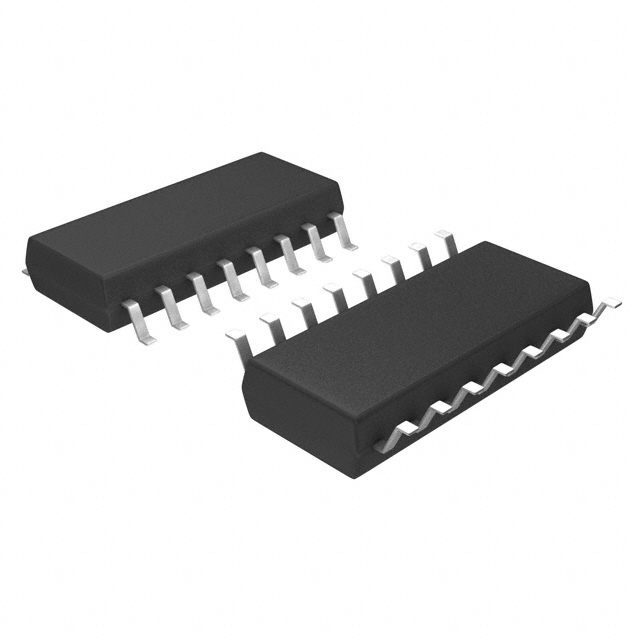
2. SO package 16-Pin type in super
miniature design
The device comes in a super-miniature
SO package 16-Pin type measuring
(W)4.4 × (L)10.37 × (H) 2.1mm (W).173 ×
(L).408 × (H).083inch
3. Ideal for PC card and Fax/Modem applications
The small size provides additional space
for increased functionality. The new device has been specifically designed for
the PCMCIA embedded and handheld
device markets.
PhotoMOS
RELAYS
4. Tape and reel
The device comes standard in tape and
reel (1,000 pcs./reel) for use with automatic insertion machines.
5. Internal zener diode type also available
TYPICAL APPLICATIONS
• PCMCIA Modem card (Data/fax modem)
• Laptop and notebook computers
• PDA's
• Mobile computing equipment
• Medical equipment
• Security systems
• Meters (Water, Gas, Vending machine)
TYPES
Type
AC/DC type
Relay portion
Output rating*
Load voltage
Load current
350V
120mA
Part No.
Picked from the 1/2/3/4/5/6/7/8-pin side
AQS210PSX
Picked from the 9/10/11/12/13/14/15/16-pin side
AQS210PSZ
Packing quantity
in tape and reel
1,000 pcs.
* Indicate the peak AC and DC values.
Notes: (1) Tape package is the standard packing style. Also available in tube. (Part No. suffix "X" or "Z" is not needed when ordering; Tube: 50 pcs.;
Case: 1,000 pcs.)
(2) For space reasons, the package type indicator "X" and "Z" are omitted from the seal.
RATING
1. Absolute maximum ratings (Ambient temperature: 25°C 77°F)
1) Relay portion (2, 3, 15, 16 pins)
Input
Output
Item
LED forward current
LED reverse voltage
Peak forward current
Power dissipation
Load voltage (peak AC)
Continuous load current
Peak load current
Power dissipation
Symbol
IF
VR
IFP
Pin
VL
IL
Ipeak
Pout
AQS210PS
50mA
3V
1A
75mW
350V
0.12A
0.36A
400mW
Symbol
IF
IFP
Pin
BVCEO
Pout
AQS210PS
50mA
1A
75mW
30V
150mW
Symbol
IF
IFP
VR
AQS210PS
140mA
500mA
100V
Remarks
f=100 Hz, Duty factor=0.1%
Peak AC,DC
100 ms (1 shot), VL= DC
2) Detector portion (7, 8, 9, 10 pins)
Input
Output
Item
LED forward current
Peak forward current
Power dissipation
Voltage between collector and emitter
Power dissipation
Remarks
f = 100 Hz, Duty factor=0.1%
3) Bridge rectifier portion (10, 11, 12, 15 pins)
Item
Forward current
Peak forward current
Reverse voltage
Remarks
t=10ms
85
�AQS210PS
4) Darlington portion (12, 13, 14 pins)
Item
Output voltage
Collector current
Power dissipation
Symbol
BVCEC
IC
Pout
AQS210PS
40V
120mA
500mW
Symbol
PT
Viso
Topr
Tstg
AQS210PS
650mW
1500V AC
–40°C to +85°C –40°F to +185°F
–40°C to +100°C –40°F to +212°F
Remarks
VCE=3.5V
5) Others
Item
Total power dissipation
I/O isolation voltage
Temperature lim- Operating
its
Storage
Remarks
Non-condensing at low temperatures
2. Electrical characteristics (Ambient temperature: 25°C 77°F)
1) Relay portion (2, 3, 15, 16 pins)
Symbol
Item
LED operate
current
Input
LED turn off
current
LED dropout
voltage
On resistance
Output
Off state leakage current
Turn on time*
Transfer characteristics
Turn off time*
Typical
Maximum
Minimum
Typical
Typical
IFon
IFoff
VF
Maximum
Typical
0.9mA
3mA
0.4mA
0.8mA
1.14 (1.25 V at IF=50mA)
1.5V
18Ω
Ron
25Ω
ILeak
1µA
Maximum
Maximum
AQS210PS
Typical
Maximum
Typical
Maximum
Ton
Toff
Condition
IL=Max.
IL=Max.
IF=5mA
IF=5mA
IL=Max.
Within 1 s on time
IF=0
VL=Max.
0.23ms
2.0ms
0.04ms
1.0ms
IF=5mA
IL=Max.
AQS210PS
Condition
2mA
IC=2mA
VCE=0.5V
IF=5mA
IL=Max.
Note: Recommendable LED forward current IF=5mA.
2) Detector portion (7, 8, 9, 10 pins)
Symbol
Item
LED operate
current
Input
Output
Typical
Maximum
Minimum
LED turn off
current
Typical
Typical
LED dropout
voltage
Maximum
Saturation volt- Typical
age
Maximum
Off state leak- Typical
age current
Maximum
Current trans- Minimum
fer ratio
Typical
IFon
IFoff
VF
Von
ICEO
—
6mA
5µA
35µA
1.14 (1.25 V at IF=50mA)
1.5V
0.08V
0.5V
0.01nA
500nA
33%
100%
Turn on time*
Typical
Ton
0.01ms
Turn off time*
Typical
Toff
0.03ms
Symbol
AQS210PS
Transfer characteristics
IC=1µA
VCE=5V
IF=5mA
IF=15mA
IC=2mA
IF=0
VCE=5V
IF=5mA
VCE=0.5V
IF=5mA
VCE=5V
IC=2mA
IF=5mA
VCE=5V
IC=2mA
3) Diode Bridge portion (10, 11, 12, 15 pins)
Item
Forward dropout voltage
Reverse leakage current
86
Typical
Maximum
Maximum
IF
IR
0.9V
1.2V
10µA
Condition
IF=120mA
VR=100V
�AQS210PS
4) Darlington transistor portion (12, 13, 14 pins)
Item
Symbol
Typical
Saturation voltage
Maximum
Maximum
Minimum
Typical
Collector leakage current
DC current gain
Total harmonic distortion
Maximum
AQS210PS
Condition
0.73V
1.5V
1µA
10,000
30,000
VCE=10V, IB=0mA
—
-80dB
IC=40mA, fo=300Hz
@-10dBm
Symbol
AQS210PS
0.8pF
1.5pF
Condition
1,000MΩ
500V DC
VCE(SAT)
ICEX
hFE
IC=120mA
IC=120mA
VCE=10V
5) Others
Item
Typical
I/O capaciMaximum
Transfer char- tance
acteristics
Initial I/O isolaMinimum
tion resistance
Ciso
Riso
—
*Turn on/Turn off time
For type of connection, see page 33.
Input
90%
10%
Output
Ton
Toff
For Dimensions, Cautions for Us, Schematics and
Wiring Diagrams, see Technical Information
REFERENCE DATA
[1] Relay portion (2, 3, 15, 16 pins) [AQS210PS]
1. Load current vs. ambient temperature characteristics
2. On resistance vs. ambient temperature characteristics
3. Turn on time vs. ambient temperature characteristics
Allowable ambient temperature: –40°C to +85°C
–40°F to +185°F
Measured portion: between terminals 15 and 16
LED current: 5 mA; Load voltage: Max. (DC);
Continuous load current: Max. (DC)
LED current: 5 mA; Load voltage: Max. (DC);
Continuous load current: Max. (DC)
50
1.0
40
0.8
100
80
60
Turn on time, ms
On resistance, Ω
Load current, mA
120
30
20
0.6
0.4
40
0.2
10
20
0
–40
–20
0
20
40
60
0
8085
–40
–20
Ambient temperature, °C
0
0
20
40
60 8085
Ambient temperature, °C
–40
–20
0
20
40
60
8085
Ambient temperature, °C
4. Turn off time vs. ambient temperature characteristics
5. LED operate current vs. ambient temperature characteristics
6. LED turn off current vs. ambient temperature
characteristics
LED current: 5 mA; Load voltage: Max. (DC);
Continuous load current: Max. (DC)
Load voltage: Max. (DC);
Continuous load current: Max. (DC)
Load voltage: Max. (DC);
Continuous load current: Max. (DC)
5
0.3
0.2
LED turn off current, mA
5
LED operate current, mA
Turn off time, ms
0.4
4
3
2
4
3
2
0.1
1
1
0
–40
–20
0
20
40
60
8085
Ambient temperature, °C
0
–40
–20
20
40
60 8085
0
Ambient temperature, °C
0
–40
–20
0
20
40
60
8085
Ambient temperature, °C
87
�AQS210PS
7. LED dropout voltage vs. ambient temperature characteristics
8. Voltage vs. current characteristics of output
at MOS portion
LED current: 5 to 50 mA
Measured portion: between terminals 15 and 16
Ambient temperature: 25°C 77°F
1.4
1.3
100
80
60
40
20
–5 –4 –3 –2 –1
50 mA
1.2
1.1
30 mA
20 mA
1 2 3 4 5
–20 Voltage, V
–40
10 mA
5 mA
–60
10–3
Off state leakage current, A
Current, mA
LED dropout voltage, V
Measured portion: between terminals 15 and 16
Ambient temperature: 25°C 77°F
120
1.5
10–6
10–9
–80
1.0
0
9. Off state leakage current
10–12
–100
–40
–20
–120
0
20
40
60
8085
Ambient temperature, °C
0
20
40
60
80
100
Load voltage, V
10. LED forward current vs. turn on time characteristics
11. LED forward current vs. turn off time characteristics
12. Applied voltage vs. output capacitance
characteristics
Measured portion: between terminals 15 and 16
Load voltage: Max. (DC); Continuous load current:
Max. (DC); Ambient temperature: 25°C 77°F
Measured portion: between terminals 15 and 16
Load voltage: Max. (DC); Continuous load current:
Max. (DC); Ambient temperature: 25°C 77°F
Measured portion: between terminals 15 and 16
Frequency: 1 MHz; Ambient temperature: 25°C 77°F
50
Output capacitance, pF
0.10
1.4
0.08
Turn off time, ms
Turn on time, ms
1.2
1.0
0.8
0.6
0.06
0.04
40
30
20
0.4
0.02
10
0.2
0
0
10
20
30
40
50
LED forward current, mA
0
0
60
10
20
30
40
50
0
0
60
10
20
30
40
50
Applied voltage, V
LED forward current, mA
[2] Detector portion (7, 8, 9, 10 pins)
1. Output loss vs. ambient temperature characteristics
2. Relative output current vs. ambient temperature characteristics
3. LED dropout voltage vs. ambient temperature characteristics
Allowable ambient temperature: –40°C to +85°C
–40°F to +185°F
Measured portion: between terminals 7 and 8
IF = 5 mA, VCE = 0.5 V DC
LED current: 5 to 50 mA
150
150
100
1.5
LED dropout voltage, V
Relative output current, %
Output loss, mW
200
100
50
1.4
1.3
50 mA
1.2
30 mA
20 mA
1.1
50
10 mA
5 mA
1.0
0
–40 –20
0
20
40
60
0
–40 –20
8085 100
Ambient temperature, °C
4-1. Collector current vs. voltage between collector and emitter characteristics (IC-VCE)
4-2. Collector current vs. voltage between collector and emitter characteristics (IC-VCE)
Measured portion: between terminals 7 and 8
Ambient temperature: 25°C 77°F
Measured portion: between terminals 7 and 8
Ambient temperature: 25°C 77°F
PC (Max.)
IF=50 mA
IF=40 mA
40
IF=30 mA
IF=10 mA
30
IF=50 mA
IF=40 mA
IF=30 mA
20
IF=20 mA
IF=10 mA
0
5/7/2001
88
2
4
6
8
10
Voltage between collector and emitter, V
10–6
10–9
10
IF=5 mA
IF=5 mA
0
0
20
40
60 8085
Ambient temperature, °C
10–3
IF=20 mA
20
–20
Measured portion: between terminals 7 and 8
IF= 0 mA
Ta= 25°C 77°F
Off state leakage current, A
60
–40
5. Off state leakage current
40
Collector current, mA
Collector current, mA
80
0
0
20
40
60
8085 100
Ambient temperature, °C
0
0
0.1
0.2
0.3
0.4
0.5
Voltage between collector and emitter, V
10–12
0
10
20
30
Voltage between collector and emitter, V
All Rights Reserved, © Copyright Matsushita Electric Works, Ltd.
�