DK
VDE
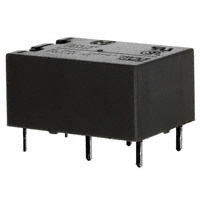
1a 10 A,1a1b/2a 8 A small
polarized power relays
DK RELAYS
FEATURES
TYPICAL APPLICATIONS
1. Compact with high capacity
High capacity switching in a small
package: 1 Form A, 10 A 250 V AC;
1 Form A 1 Form B and 2 Form A, 8 A
250 V AC.
2. High sensitivity: 200 mW nominal
operating power
3. High breakdown voltage
Independent coil and the contact
structure improves breakdown voltage.
1. Switching power supply
2. Power switching for various
OA equipment
3. Control or driving relays for
industrial machines (robotics,
numerical control machines, etc.)
4. Output relays for programmable
logic controllers, temperature
controllers, timers and so on.
5. Home appliances
Between contact
and coil
Between open contacts
4,000 Vrms for 1 min.
10,000 V surge
breakdown voltage
1,000 Vrms for 1 min.
1,500 V surge
breakdown voltage
Conforms with FCC Part 68
4. Latching types available
5. Sealed construction allows
automatic washing.
6. High insulation resistance
Creepage distance and clearances
between contact and coil: Min. 8 mm
DK2a-L2: 6.8 mm
DK1a1b-L2: 6.8 mm
7. Sockets are available
8. Complies with safety standards
Complies with Japan Electrical
Appliance and Material Safety Law
requirements for operating 200 V
power supply circuits, and complies
with UL, CSA, and TÜV safety
standards.
About Cd-free contacts
We have introduced Cadmium free type
products to reduce Environmental
Hazardous Substances.
(The suffix “F” should be added to the
part number)
(Note: The Suffix “F” is required only for
1 Form A contact type. The 2 Form A and
1 Form A 1 Form B contact type is
originally Cadmium free, the suffix “F” is
not required.)
Please replace parts containing
Cadmium with Cadmium-free products
and evaluate them with your actual
application before use because the life of
a relay depends on the contact material
and load.
ORDERING INFORMATION
DK
Contact arrangement
1a: 1 Form A
2a: 2 Form A
1a1b: 1 Form A 1 Form B
Operating function
Nil: Single side stable
L: 1 coil latching
L2: 2 coil latching
Coil voltage (DC)
3, 5, 6, 9, 12, 24V
Contact material
F: 1 Form A (AgSnO2 type)
Nil: 2 Form A, 1 Form A 1 Form B (Au-flashed AgNi type)
Notes: 1. UL/CSA, TÜV approved type is standard.
2. VDE approved type is available.
1
ds_61A03_en_dk: 201113D
�DK
TYPES
Contact
arrangement
Single side stable
1 coil latching
2 coil latching
Part No.
Part No.
Part No.
3V DC
DK1a-3V-F
DK1a-L-3V-F
DK1a-L2-3V-F
5V DC
DK1a-5V-F
DK1a-L-5V-F
DK1a-L2-5V-F
6V DC
DK1a-6V-F
DK1a-L-6V-F
DK1a-L2-6V-F
9V DC
DK1a-9V-F
DK1a-L-9V-F
DK1a-L2-9V-F
12V DC
DK1a-12V-F
DK1a-L-12V-F
DK1a-L2-12V-F
24V DC
DK1a-24V-F
DK1a-L-24V-F
DK1a-L2-24V-F
3V DC
DK1a1b-3V
DK1a1b-L-3V
DK1a1b-L2-3V
5V DC
DK1a1b-5V
DK1a1b-L-5V
DK1a1b-L2-5V
6V DC
DK1a1b-6V
DK1a1b-L-6V
DK1a1b-L2-6V
9V DC
DK1a1b-9V
DK1a1b-L-9V
DK1a1b-L2-9V
12V DC
DK1a1b-12V
DK1a1b-L-12V
DK1a1b-L2-12V
24V DC
DK1a1b-24V
DK1a1b-L-24V
DK1a1b-L2-24V
3V DC
DK2a-3V
DK2a-L-3V
DK2a-L2-3V
5V DC
DK2a-5V
DK2a-L-5V
DK2a-L2-5V
6V DC
DK2a-6V
DK2a-L-6V
DK2a-L2-6V
9V DC
DK2a-9V
DK2a-L-9V
DK2a-L2-9V
12V DC
DK2a-12V
DK2a-L-12V
DK2a-L2-12V
24V DC
DK2a-24V
DK2a-L-24V
DK2a-L2-24V
Nominal coil
voltage
1 Form A
1 Form A
1 Form B
2 Form A
Standard packing: Carton: 50 pcs.; Case: 500 pcs.
* For sockets, see page 8.
RATING
1. Coil data
1) Single side stable
Nominal coil
voltage
Pick-up voltage
(at 20C 68F)
Drop-out voltage
(at 20C 68F)
Nominal operating
current
[10%] (at 20C 68F)
Coil resistance
[10%] (at 20C 68F)
3V DC
66.6mA
45
5V DC
40mA
125
33.3mA
180
22.2mA
405
6V DC
9V DC
70%V or less of
nominal voltage
(Initial)
10%V or more of
nominal voltage
(Initial)
12V DC
16.6mA
720
24V DC
8.3mA
2,880
Nominal operating
current
[10%] (at 20C 68F)
Coil resistance
[10%] (at 20C 68F)
Nominal operating
power
Max. applied voltage
(at 20C 68F)
200mW
130%V of
nominal voltage
Nominal operating
power
Max. applied voltage
(at 20C 68F)
100mW
130%V of
nominal voltage
2) 1 coil latching
Nominal coil
voltage
Set voltage
(at 20C 68F)
Reset voltage
(at 20C 68F)
3V DC
33.3mA
90
5V DC
20mA
250
16.6mA
360
11.1mA
810
12V DC
8.3mA
1,440
24V DC
4.1mA
5,760
Nominal operating
current
[10%] (at 20C 68F)
Coil resistance
[10%] (at 20C 68F)
6V DC
9V DC
70%V or less of
nominal voltage
(Initial)
70%V or more of
nominal voltage
(Initial)
3) 2 coil latching
Nominal coil
voltage
Set voltage
(at 20C 68F)
Reset voltage
(at 20C 68F)
3V DC
5V DC
Set coil
Reset coil
Set coil
Reset coil
66.6mA
66.6mA
45
45
40mA
40mA
125
125
33.3mA
33.3mA
180
180
22.2mA
22.2mA
405
405
12V DC
16.6mA
16.6mA
720
720
24V DC
8.3mA
8.3mA
2,880
2,880
6V DC
9V DC
70%V or less of
nominal voltage
(Initial)
ds_61A03_en_dk: 201113D
70%V or less of
nominal voltage
(Initial)
Nominal operating
power
Set coil
Reset coil
200mW
200mW
Max. applied voltage
(at 20C 68F)
130%V of
nominal voltage
2
�DK
2. Specifications
Characteristics
Item
Arrangement
Contact
1 Form A 1 Form B
Contact resistance (Initial)
Au-flashed AgSnO2 type
Nominal switching capacity (resistive load)
10 A 250 V AC, 10 A 30 V
DC
2,000 VA, 240 W
2,000 VA, 240 W
250 V AC, 125 V DC
250 V AC, 125 V DC
Max. switching current
10 A
8A
8A
Breakdown voltage
(Initial)
200 mW
Surge breakdown
voltage*2 (Initial)
10m A 5 V DC
Min. 1,000M (at 500V DC) Measurement at same location as “Breakdown voltage” section.
Between open contacts
1,000 Vrms for 1min. (Detection current: 10mA.)
Between contact and coil
4,000 Vrms for 1min. (Detection current: 10mA.)
between contacts and coil
10,000 V
Temperature rise (coil) (at 65C 149F)
Max. 40C (By resistive method, nominal voltage applied to the coil; max. switching current)
Operate time [Set time] (at 20C 68F)
Max. 10 ms (Approx. 5 ms) [10 ms (Approx. 5 ms)]
(Nominal coil voltage applied to the coil, excluding contact bounce time.)
Release time [Reset time] (at 20C 68F)
Shock resistance
Mechanical
characteristics
Vibration resistance
Functional
Max. 8 ms (Approx. 3 ms) [10 ms (Approx. 3 ms)]
(Nominal coil voltage applied to the coil, excluding contact bounce time.) (without diode)
Min. 98 m/s2 (Half-wave pulse of sine wave: 11 ms; detection time: 10s.)
Destructive
Min. 980 m/s2 (Half-wave pulse of sine wave: 6 ms.)
Functional
10 to 55 Hz at double amplitude of 1.5 mm (Detection time: 10s.)
Destructive
10 to 55 Hz at double amplitude of 3 mm
Mechanical
Electrical
Conditions for operation, transport and storage*3
Min. 5107 (at 300 times/min.)
Min. 105 (resistive load, at 20 times/min., at rated capacity)
Ambient temperature: –40C to +65C –40F to +149F,
Humidity: 5 to 85% R.H. (Not freezing and condensing at low temperature)
Max. operating speed (at rated load)
Unit weight
8 A 250 V AC,8 A 30 V DC
2,500VA, 300 W
Insulation resistance (Initial)
Conditions
8 A 250 V AC,8 A 30 V DC
250 V AC, 125 V DC
Min. switching capacity (Reference value)*1
Expected life
Au-flashed AgNi type
Max. switching voltage
Nominal operating power
Electrical
characteristics
2 Form A
Max. 30 m (By voltage drop 6 V DC 1A)
Contact material
Max. switching power (resistive load)
Rating
Specifications
1 Form A
20 times/min.
Approx. 5 g .18 oz
Approx. 6 g .21 oz
Approx. 6 g .21 oz
Notes:
*1. This value can change due to the switching frequency, environmental conditions, and desired reliability level, therefore it is recommended to check this with the actual load.
*2. Wave is standard shock voltage of 1.250s according to JEC-212-1981
*3. The upper limit of the ambient temperature is the maximum temperature that can satisfy the coil temperature rise value. Refer to “6. Usage, Storage and Transport
Conditions“ in AMBIENT ENVIRONMENT section in Relay Technical Information.
3
ds_61A03_en_dk: 201113D
�DK
REFERENCE DATA
1-(1). Maximum operating power (1 Form A)
1-(2). Maximum operating power
(1 Form A 1 Form B, 2 Form A)
2-(1). Life curve (1 Form A)
1,000
AC resistive load
DC inductive load
(L/R = 7 ms)
1
0.1
10
DC resistive
load
100
Contact voltage, V
AC inductive load
(cosϕ = 0.4) AC resistive load
10
5
DC inductive load
(L/R = 7 ms)
1
0.1
1,000
Life, ×104
AC inductive load
(cosϕ = 0.4)
10
Contact current, A
Contact current, A
100
10
DC resistive
load
100
100
250 V AC resistive load
30 V DC resistive load
10
1
1,000
250 V AC inductive load (cosϕ= 0.4)
30 V DC inductive load (L/R = 7 ms)
0
1
2
3
4
Contact voltage, V
2-(2). Life curve
(1 Form A 1 Form B, 2 Form A)
5
6
7
8
9
10
Contact current, A
3-(1). Operate/Release time (1 Form A)
Tested sample: DK1a-24V, 5 pcs.
3-(2). Operate/Release time
(1 Form A 1 Form B, 2 Form A)
Tested sample: DK1a1b-12V, 5 pcs.
1,000
9
9
100
250 V AC resistive load
30 V DC resistive load
10
250 V AC inductive load (cosϕ = 0.4)
30 V DC inductive load (L/R = 7 ms)
6
5
4
Release time
(with diode)
3
0
1
2
3
4
5
6
7
8
9
0
10
90
40
10A
7A
5A
0A
20
10
100 110 120 130
Coil applied voltage,%V
Max.
x
Min.
Max.
x
Min.
Operate time
3
Release time
1
120
130
140
0
80
90
10
110
120
130
140
Coil applied voltage,%V
5-(1). Ambient temperature characteristics
(1 Form A)
Tested sample: DK1a1b-12V, 5 pcs.
Ambient temperature: 20C 68F
Tested sample: DK1a-24V, 6 pcs
Ambient temperature: –40C to +80C
–40F to +176F
50
40
8A
5A
0A
30
20
0
130
Drop-out
voltage
120
110
100
-40
-20
0
20
90
10
90
4
Variation ratio, %
50
80
5
4-(2). Coil temperature rise
(1 Form A 1 Form B, 2 Form A)
Coil temperature rise, °C
4-(1). Coil temperature rise (1 Form A)
Coil temperature rise, °C
110
6
Coil applied voltage,%V
Tested sample: DK1a-12V, 5 pcs.
Ambient temperature: 30C 86F
0
10
Max.
x
Min.
7
2
Release time
80
Contact current, A
30
Max.
x
Max.
x
Min.
Min.
Max.
x
Min.
2
1
1
Release time
(with diode)
8
Operate time
7
Operate/release time, ms
Operate/release time, ms
Life, ×104
8
Pick-up
voltage
40
60
80
Ambient
temperature, °C
80
80
90
100 110 120 130
70
Coil applied voltage,%V
Variation ratio, %
5-(2). Ambient temperature characteristics
(1 Form A 1 Form B, 2 Form A)
-40 -20
Pick-up
voltage
130
120
110
0 100
40
20
90
80
60
80
Ambient
temperature,°C
Drop-out
voltage
70
ds_61A03_en_dk: 201113D
4
�DK
DIMENSIONS (mm inch)
CAD Data
Data from our Web site.
Download CAD
1. 1 Form A type
External dimensions
CAD Data
PC board pattern (Bottom view)
Single side stable type
20
.787
12.5
.492
2.54
.100
7.62
.300
7.62
.300
2.54
.100
7.62
.300
7.62
.300
1.1 dia.
.043 dia.
9.7
.382
0.3
.012
3.5
.138
0.4
.016
0.8
.031
10.16
.400
7.62
.300
0.4
.016
0.8
.031
1.11
.044
1.2
.047
10.16
.400
10.16
.400
2 coil latching type
20
.787
12.5
.492
1.1 dia.
.043 dia.
9.7
.382
0.3
.012
3.5
.138
0.4
.016
2.54
.100
0.4
.016
7.62
.300
0.8
.031
7.62
.300
0.4
.016
0.8
.031
1.11
.044
1.2
.047
10.16
.400
10.16
.400
General tolerance: 0.3 .012
Tolerance: 0.1 .004
Schematic (Bottom view)
Single side stable
1
-
3
4
+
6
(Deenergized condition)
1 coil latching
1
+
3
4
6
(Reset condition)
2 coil latching
1
-
3
+
+
6
5
4
(Reset condition)
Since this is a polarized relay, the connection to the coil
should be done according to the above schematic.
5
ds_61A03_en_dk: 201113D
�DK
2. 1 Form A 1 Form B type, 2 Form A type
External dimensions
CAD Data
PC board pattern (Bottom view)
Single side stable type
20
.787
15
.591
10.16
.400
1.1 dia.
.043 dia.
7.62
.300
9.7
.382
0.3
.012
0.4
.016
0.8
.031
10.16
.400
3.5
.138
0.8
.031
2.42
1.11
.044
.095
7.62
.300
10.16
.400
10.16
.400
0.4
.016
2 coil latching type
20
.787
15
.591
2.54
.100
7.62
.300
1.1 dia.
.043 dia.
7.62
.300
9.7
.382
0.3
.012
0.4
.016
2.54
.100
0.6
.024
7.62
.300
3.5
.138
0.8
.031
2.42
1.11
.044
.095
0.8
.031
7.62
.300
10.16
.400
10.16
.400
0.4
.016
General tolerance: 0.3 .012
Tolerance: 0.1 .004
Schematic (Bottom view)
Schematic (Bottom view)
Single side stable
Single side stable
1
-
3
4
6
5
1
-
+
3
4
6
5
+
8
8
(Deenergized condition)
(Deenergized condition)
1 coil latching
1 coil latching
1
3
4
6
5
1
3
4
6
5
+
+
-
8
8
(Reset condition)
(Reset condition)
2 coil latching
2 coil latching
1
+
+
8
7
3
4
6
5
1
+
+
8
7
3
4
6
5
(Reset condition)
(Reset condition)
Since this is a polarized relay, the connection to the coil should be done
according to the above schematic.
SAFETY STANDARDS
Item
UL/C-UL (Recognized)
File No.
CSA (Certified)
File No.
Contact rating
VDE (Certified)
File No.
Contact rating
TÜV (Certified)
File No.
Rating
E43028
10A 250V AC
LR26550
1/3HP 125, 250V AC
etc.
10A 30V DC
10A 250V AC
006099UG AC 250V 10A (cos =1.0) 8705
1/3HP 125, 250V AC
AC 250V 5A (cos=0.4) 1645 520
10A 30V DC
DC 30V 10A (0ms)
10A 250V AC (cos =1.0)
5A 250V AC (cos=0.4)
10A 30V DC
E43028
LR26550
8A 250V AC
1/4HP 125, 250V AC
etc.
8A 30V DC
1 4
8A 250V AC
006099UG 1 Form A 1 Form B:
/ HP 125, 250V AC
AC 250V 8A (cos=1.0)
8A 30V DC
2 Form A:
AC 250V 8A (cos =1.0)
AC 250V 4A (cos =0.4)
8A 250V AC (cos =1.0)
4A 250V AC (cos =0.4)
8A 30V DC
1 Form A
1 Form A
1 Form B,
2 Form A
Contact rating
ds_61A03_en_dk: 201113D
8705 1645
520 (1 Form A
1 Form B)
9407 13461
097 (2 Form A)
6
�DK
NOTES
1. Soldering should be done under the
following conditions:
250C 482F within 10s
300C 572F within 5s
350C 662F within 3s
Soldering depth: 2/3 terminal pitch
2. External magnetic field
Since DK relays are highly sensitive
polarized relays, their characteristics will
be affected by a strong external magnetic
field. Avoid using the relay under that
condition.
3. When using, please be aware that
the a contact and b contact sides of 1
Form A and 1 Form B types may go on
simultaneously at operate time and
release time.
For Cautions for Use, see Relay Technical Information.
7
ds_61A03_en_dk: 201113D
�DK
DK RELAY
SOCKET
ACCESSORIES
FEATURES
TYPES
DK relay sockets that can be used also
for DY relay.
Type
Part No.
Single side
stable
1 Form A
DK1a-PS
2 coil
latching
1 Form A 1 Form B,
2 Form A*
DK1a-PSL2
Single side
stable
DK2a-PS
2 coil
latching
DK2a-PSL2
Standard packing: Carton: 50 pcs.; Case: 500 pcs
Note: * 2 Form A type is DK relays only.
RELAY COMPATIBILITY
SPECIFICATIONS
1 Form A
Socket
Relay
Single side stable type
1 Form A
1 Form A 1 Form B
2 Form A
1 Form A 1 Form B, 2 Form A
Single side
stable type
2 coil
latching type
Single side
stable type
2 coil
latching type
—
—
Item
Specifications
Breakdown
voltage
4,000 Vrms
(Detection current: 10 mA)
(Except the portion between
coil terminals)
2 coil latching type
—
—
—
Single side stable type
—
—
Insulation
resistance
Min. 1,000 m (at 500 V DC)
2 coil latching type
—
—
—
Heat resistance
150C (for 1 hour)
Max. continuous
current
10 A (DK1a-PS, DK1a-PSL2),
8 A (DK2a-PS, DK2a-PSL2)
DIMENSIONS (mm inch)
External dimensions
PC board pattern (Bottom view)
1 Form A
15±0.6
.591±.024
1
2
6
5
3
1 Form A 1 Form B
4
1.2 dia.
.047 dia.
1
2
3
4
8
7
6
5
1.2 dia.
.047 dia.
23±0.6
.906±.024
2.54
.100
2.54
.100
17±0.6
.669±.024
13.7±0.6
.539±.024
Tolerance: 0.1 .004
6±0.3
.236±.012
0.3±0.1
.012±.004
2.54±0.1
.100±.004
0.8
.031
7.62±0.3 7.62±0.3
.300±.012 .300±.012
3.4±0.3
.134±.012
2.54
.100
2.54
.100
0.25
.010
10.16±0.3
.400±.012
The above shows 2 coil latching type. No.2 and 5
terminal are eliminated on single side stable type.
The above shows 2 coil latching type. No.2 and 7
terminal are eliminated on single side stable type.
General tolerance: 0.3 .012
ds_61A03_en_dk: 201113D
8
�DK
FIXING AND REMOVAL METHOD
1. Match the direction of relay and
socket.
3. Remove the relay, applying force in the
direction shown below.
2. Both ends of the relay are to be
secured firmly so that the socket hooks
on the top surface of the relay.
4. In case there is not enough space to
grasp the relay with fingers, use
screwdrivers in the way shown in the
illustration.
GOOD
9
Notes: 1. Exercise care when removing relays. If
greater than necessary force is applied at
the socket hooks, deformation may alter the
dimensions so that the hook will no longer
catch, and other damage may also occur.
2. It is hazardous to use IC chip sockets.
NO GOOD
ds_61A03_en_dk: 201113D
�


 工商网监
湘ICP备2023018690号
工商网监
湘ICP备2023018690号
