Power Inductors
Multilayer Power Inductors
Discontinued
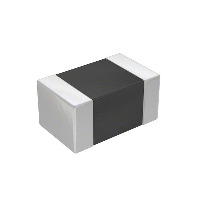
Type: ELGTEA
Features
●Superior DC current bias characteristics by the original laminating process technology
●Magnetic shielded structure
●Small and thin structure (2.0×1.25×1.0mm max.)
●RoHS compliant
Recommended applications
●DC/DC converter circuit use of the small portable device
Smart phone, mobile phone, DSC .
Standard packing quantity
●4,000 pcs / Reel
Explanation of part numbers
1
2
3
4
5
6
7
8
9
10
11
E
L
G
T
E
A
1
R
0
N
A
shape
Height
Construction
Product Code
Nominal inductance
Inductance
12
Design code
(Example)
Code
T
Size
2012 mm
(0805 inch)
T dimension
Code
Height
E
1.0 mm max.
Code
Construction
Code Inductance
A
Multilayer
power inductor
R47
0.47 μH
2R2
2.2 μH
N
±30 %
Recommended land patterns
1.1 to 1.3
Dimensions
Code Tolerance
0.8 ±0.20
0.45 ±0.20
0.8 to 1.2
1.25 ±0.20
2.00 ±0.20
Unit : mm
Unit : mm
2.4 to 3.0
Ratings and characteristics
Part No.
Inductance at 1 MHz
DC Resistance
at 20 ℃
Rated Current
✽1
Self-resonant
Frequency
(μH)
Tol. (%)
(Ω) max.
(A)
(MHz)
ELGTEAR47NA
0.47
±30
0.10
1.2
126
ELGTEA1R0NA
1.0
±30
0.15
1.0
80
ELGTEA1R5NA
1.5
±30
0.18
1.0
80
ELGTEA2R2NA
2.2
±30
0.20
0.8
55
ELGTEA3R3NA
3.3
±30
0.25
0.8
50
ELGTEA4R7NA
4.7
±30
0.30
0.8
33
✽2
● Operating Temperature Range:-40 to 125 ℃ (Including self-temperature rise)
✽1 This indicates the value of current when temperature rise dt/t=40 ℃ (at 20 ℃).
✽2 Reference data
Design and specifications are each subject to change without notice. Ask factory for the current technical specifications before purchase and/or use.
Should a safety concern arise regarding this product, please be sure to contact us immediately.
1-Apr-21
�Power Inductors
DC current bias characteristics
Inductance frequency characteristics
10
6.0
9
5.0
7
Inductance (μH)
Inductance (μH)
8
6
4.7 µH
5
4
3.3 µH
3
2.2 µH
2
1.5 µH
3.3 µH
3.0
2.0
2.2 µH
1.5 µH
1.0
1
1.0 µH
0
0.01
4.7 µH
4.0
0.47 µH
0.1
1
10
1.0 µH
0
0.0
100
0.47 µH
0.5
1.0
Frequency (MHz)
1.5
2.0
DC Current (A)
Packaging methods (Taping)
● Punched Carrier Taping (Pitch 4mm)
Feeding hole
øD0
W1
E
Chip pocket
E
C
B
P1
t2
D
F
W
A
B
t1
● Taping Reel
P2
P0
W2
Tape running direction
Chip component
A
Unit : mm
Symbol
Size
A
B
W
F
P1
E
P2
P0
1.65
2.4
8.0
3.50
1.75
4.0
2.00
4.0
±0.20
±0.2
±0.2
±0.05
±0.10
±0.1
±0.05
±0.1
● Leader Part and Taped End
øD0
1.5
+0.1
0
t1
t2
1.2
1.4
max
max
Unit : mm
Symbol
Size
A
ø180
B
0
-3
φ 60.0
+1.0
0
C
D
E
13.0±0.5 21.0±0.8
2.0±0.5
W1
9.0
W2
+1.0
0
11.4±1.0
Tape end
Leader part
Cover tape
100 min.
Vacant position
400 min.
160 min.
Vacant position
Unit : mm
Design and specifications are each subject to change without notice. Ask factory for the current technical specifications before purchase and/or use.
Should a safety concern arise regarding this product, please be sure to contact us immediately.
1-Apr-21
�*XLGHOLQHV�DQG�SUHFDXWLRQV�UHJDUGLQJ�WKH
WHFKQLFDO�LQIRUPDWLRQ�DQG�XVH�RI�RXU�SURGXFWV
GHVFULEHG�LQ�WKLV�RQOLQH�FDWDORJ�
�ٹ,I�\RX�ZDQW�WR�XVH�RXU�SURGXFWV�GHVFULEHG�LQ�WKLV�RQOLQH�FDWDORJ�IRU�DSSOLFDWLRQV�UHTXLULQJ�
�VSHFLDO�TXDOLWLHV�RU�UHOLDELOLW\��RU�IRU�DSSOLFDWLRQV�ZKHUH�WKH�IDLOXUH�RU�PDOIXQFWLRQ�RI�WKH�
�SURGXFWV�PD\�GLUHFWO\�MHRSDUGL]H�KXPDQ�OLIH�RU�SRWHQWLDOO\�FDXVH�SHUVRQDO�LQMXU\�
��H�J��DLUFUDIW�DQG�DHURVSDFH�HTXLSPHQW��WUDIILF�DQG�WUDQVSRUWDWLRQ�HTXLSPHQW��FRPEXVWLRQ�
�HTXLSPHQW��PHGLFDO�HTXLSPHQW��DFFLGHQW�SUHYHQWLRQ��DQWL�FULPH�HTXLSPHQW��DQG�RU�VDIHW\�
�HTXLSPHQW���LW�LV�QHFHVVDU\�WR�YHULI\�ZKHWKHU�WKH�VSHFLILFDWLRQV�RI�RXU�SURGXFWV�ILW�WR�VXFK�
�DSSOLFDWLRQV��3OHDVH�HQVXUH�WKDW�\RX�ZLOO�DVN�DQG�FKHFN�ZLWK�RXU�LQTXLU\�GHVN�DV�WR�ZKHWKHU
�WKH�VSHFLILFDWLRQV�RI�RXU�SURGXFWV�ILW�WR�VXFK�DSSOLFDWLRQV�XVH�EHIRUH�\RX�XVH�RXU�SURGXFWV�
�ٹ7KH�TXDOLW\�DQG�SHUIRUPDQFH�RI�RXU�SURGXFWV�DV�GHVFULEHG�LQ�WKLV�RQOLQH�FDWDORJ�RQO\�DSSO\�
�WR�RXU�SURGXFWV�ZKHQ�XVHG�LQ�LVRODWLRQ��7KHUHIRUH��SOHDVH�HQVXUH�\RX�HYDOXDWH�DQG�YHULI\�
�RXU�SURGXFWV�XQGHU�WKH�VSHFLILF�FLUFXPVWDQFHV�LQ�ZKLFK�RXU�SURGXFWV�DUH�DVVHPEOHG�LQ�\RXU�
�RZQ�SURGXFWV�DQG�LQ�ZKLFK�RXU�SURGXFWV�ZLOO�DFWXDOO\�EH�XVHG�
�ٹ,I�\RX�XVH�RXU�SURGXFWV�LQ�HTXLSPHQW�WKDW�UHTXLUHV�D�KLJK�GHJUHH�RI�UHOLDELOLW\��UHJDUGOHVV�
�RI�WKH�DSSOLFDWLRQ��LW�LV�UHFRPPHQGHG�WKDW�\RX�VHW�XS�SURWHFWLRQ�FLUFXLWV�DQG�UHGXQGDQF\�
�FLUFXLWV�LQ�RUGHU�WR�HQVXUH�VDIHW\�RI�\RXU�HTXLSPHQW�
�ٹ7KH�SURGXFWV�DQG�SURGXFW�VSHFLILFDWLRQV�GHVFULEHG�LQ�WKLV�RQOLQH�FDWDORJ�DUH�VXEMHFW�WR�
�FKDQJH�IRU�LPSURYHPHQW�ZLWKRXW�SULRU�QRWLFH��7KHUHIRUH��SOHDVH�EH�VXUH�WR�UHTXHVW�DQG�
�FRQILUP�WKH�ODWHVW�SURGXFW�VSHFLILFDWLRQV�ZKLFK�H[SODLQ�WKH�VSHFLILFDWLRQV�RI�RXU�SURGXFWV�LQ�
�GHWDLO��EHIRUH�\RX�ILQDOL]H�WKH�GHVLJQ�RI�\RXU�DSSOLFDWLRQV��SXUFKDVH��RU�XVH�RXU�SURGXFWV�
�ٹ7KH�WHFKQLFDO�LQIRUPDWLRQ�LQ�WKLV�RQOLQH�FDWDORJ�SURYLGHV�H[DPSOHV�RI�RXU�SURGXFWV
�
�W\SLFDO�RSHUDWLRQV�DQG�DSSOLFDWLRQ�FLUFXLWV��:H�GR�QRW�JXDUDQWHH�WKH�QRQ�LQIULQJHPHQW�RI�
�WKLUG�SDUW\
V�LQWHOOHFWXDO�SURSHUW\�ULJKWV�DQG�ZH�GR�QRW�JUDQW�DQ\�OLFHQVH��ULJKW��RU�LQWHUHVW�
LQ�RXU�LQWHOOHFWXDO�SURSHUW\�
�ٹ,I�DQ\�RI�RXU�SURGXFWV��SURGXFW�VSHFLILFDWLRQV�DQG�RU�WHFKQLFDO�LQIRUPDWLRQ�LQ�WKLV�RQOLQH�
�FDWDORJ�LV�WR�EH�H[SRUWHG�RU�SURYLGHG�WR�QRQ�UHVLGHQWV��WKH�ODZV�DQG�UHJXODWLRQV�RI�WKH�
�H[SRUWLQJ�FRXQWU\��HVSHFLDOO\�ZLWK�UHJDUG�WR�VHFXULW\�DQG�H[SRUW�FRQWURO��VKDOO�EH�REVHUYHG��
�5HJDUGLQJ�WKH�&HUWLILFDWH�RI�&RPSOLDQFH�ZLWK�
WKH�(8�5R+6�'LUHFWLYH�5($&+�5HJXODWLRQV!
�ٹ7KH�VZLWFKRYHU�GDWH�IRU�FRPSOLDQFH�ZLWK�WKH�5R+6�'LUHFWLYH�5($&+�5HJXODWLRQV�YDULHV�
�GHSHQGLQJ�RQ�WKH�SDUW�QXPEHU�RU�VHULHV�RI�RXU�SURGXFWV�
�ٹ:KHQ�\RX�XVH�WKH�LQYHQWRU\�RI�RXU�SURGXFWV�IRU�ZKLFK�LW�LV�XQFOHDU�ZKHWKHU�WKRVH�SURGXFWV�
�DUH�FRPSOLDQW�ZLWK�WKH�5R+6�'LUHFWLYH�5($&+�5HJXODWLRQ��SOHDVH�VHOHFW��6DOHV�,QTXLU\��LQ�WKH�
�ZHEVLWH�LQTXLU\�IRUP�DQG�FRQWDFW�XV�
:H�GR�QRW�WDNH�DQ\�UHVSRQVLELOLW\�IRU�WKH�XVH�RI�RXU�SURGXFWV�RXWVLGH�WKH�VFRSH�RI�WKH�
VSHFLILFDWLRQV��GHVFULSWLRQV��JXLGHOLQHV�DQG�SUHFDXWLRQV�GHVFULEHG�LQ�WKLV�RQOLQH�FDWDORJ�
���$SU���
�Power Inductors
Multilayer Power Inductors
Type: ELGTEA, ELGUEB
Handling Precautions
[Precautions]
・ Do not use the products beyond the descriptions in this product catalog.
・ This product catalog guarantees the quality of the products as individual components.
Before you use the products, please make sure to check and evaluate the products
in the circumstance where they are installed in your product.
Safety Precautions
Multilayer Power Inductors (hereafter referred to as “Inductors”) should be used for general purpose
applications in consumer electronics (audio/visual, home, office, information & communication) equipment.
When subjected to severe electrical, environmental, and/or mechanical stress beyond the specifications, as
noted in the Ratings and Specified Conditions section, the Inductors may fail in a short circuit mode or in an
open-circuit mode.
This case results in a burn-out, smoke or flaming.
For products which require high safety levels, please carefully consider how a single malfunction can
affect your product. In order to ensure the safety in the case of a single malfunction, please design products
with fail-safe, such as setting up protecting circuits, etc.
● For the following applications and conditions, please contact us for additional specifications not found in this
document.
・ When your application may have difficulty complying with the safety or handling precautions specified below.
・ For any applications where a malfunction with this product may directly or indirectly cause hazardous
conditions which could result in death or injury;
① Aircraft and Aerospace Equipment (artificial satellite, rocket, etc.)
② Submarine Equipment (submarine repeating equipment, etc.)
③ Transportation Equipment (motor vehicles, airplanes, trains, ship, traffic signal controllers, etc.)
④ Power Generation Control Equipment
(atomic power, hydroelectric power, thermal power plant control system, etc.)
⑤ Medical Equipment (life-support equipment, pacemakers, dialysis controllers, etc.)
⑥ Information Processing Equipment (large scale computer systems, etc.)
⑦ Electric Heating Appliances, Combustion devices (gas fan heaters, oil fan heaters, etc.)
⑧ Rotary Motion Equipment
⑨ Security Systems
⑩ And any similar types of equipment
Strict Observance
1. Confirmation of Rated Performance
The Inductors shall be operated within the specified rating/performance.
Applications exceeding the specifications may cause deteriorated performance and/or breakdown, resulting in
degradation and/or smoking or ignition of products. The following are strictly observed.
(1) The Inductors should be use within the specified operating temperature range including self-fever.
(2) The electricity electric current of the inductor should be use in less than rated current.
2. The Inductors shall not be mounted near flammables.
3. The Inductors shall not be bring a magnet and the thing which became magnetized
close.
01-Oct-19
�Power Inductors
Operating Conditions and Circuit Design
1. Circuit Design
1.1 Operating Temperature and Storage Temperature
The specified “Operating Temperature Range” found in the Specification is the absolute maximum and minimum
temperature rating. Every Inductor shall be operated within the specified “Operating Temperature Range”.
The Inductors mounted on PWB shall be stored without operating within the specified “Storage Temperature
Range” in the Specifications.
1.2 Operating Current
The Inductors shall not be operated in excess of the “Rated current”. If the Inductors are operated
beyond the specified “Rated current", it may cause short and/or damage due to thermal run away.
When high frequency and steep pulse current are continuously used, even when less than the “Rated current”,
in a circuit, please examine the reliability of the Inductor while also checking the safety and reliability of your circuit.
Check safety and reliability in your circuit.
1.3 Self-heating
The surface temperature of the Inductors shall be under the specified Maximum Operating Temperature in the
Specifications including the temperature rise cause by self-heating. Check temperature rise of the Inductors
in your circuit.
1.4 Environmental Restrictions
The Inductors shall not be operated and/or stored under the following conditions.
(1) Environmental conditions
(a) Under direct exposure to water or salt water
(b) Under conditions where water can condense and/or dew can form
(c) Under conditions containing corrosive gases such as hydrogen sulfide, sulfurous acid, chlorine and ammonia
(2) Mechanical conditions
Under severe conditions of vibration or impact beyond the specified conditions found in the Specifications.
2. Design of Printed Circuit Board
2.1 Selection of Printed Circuit Boards
When the Inductors are mounted and soldered on an “Alumina Substrate”, the substrate influences the Inductors’
reliability against “Temperature Cycles” and “Heat shock” due to the difference in the thermal expansion coefficient
between them.
Confirm that the actual board used does not deteriorate the characteristics of the Inductors.
2.2 Design of Land Pattern
1) Recommended land dimensions are shown below. Use the proper amount of solder in order to prevent cracking.
Using too much solder places excessive stress on the Inductors.
Recommended Land Dimensions(Ex.)
SMD
c
Land
b
Solder resist
Size
Code/EIA
Unit (mm)
Component dimensions
a
b
c
1.0 max.
0.8 to 1.2
0.6 to 1.1
1.1 to 1.3
1.0 max.
0.8 to 1.2
0.6 to 1.1
1.2 to 1.4
L
W
T
T(0805)
2.0
1.25
U(0806)
2.0
1.60
a
01-Oct-19
�Power Inductors
(2) The land size shall be designed to have equal space, on both right and left side. If the amount of solder on
the right land is different from that of the left land, the component may be cracked by stress since the side
with a larger amount of solder solidifies later during cooling.
Recommended Amount of Solder
(a) Excessive amount
(b) Proper amount
2.3 Utilization of Solder Resist
(1) Solder resist shall be utilized to equalize
the amounts of solder on both sides.
(2) Solder resist shall be used to divide the
pattern for the following cases;
・ Components are arranged closely.
・ The Inductors is mounted near
(c) Insufficient amount
Prohibited Applications and Recommended Applications
Mixed
mounting
with a
component
with lead
wires
See the table right.
by pattern division
The lead wire of a Component
With lead wires
a component with lead wires.
・ The Inductors is placed near a chassis.
Improved applications
Prohibited
applications
Item
Chassis
Arrangement
near
chassis
Solder(ground solder)
Solder resist
Solder resist
Electrode pattern
Retro-fitting
of component
with lead
wires
A lead wire of Retrofitted
component
Solderingiron
iron
Portion to be
Lateral
arrangement
Solder resist
Excessively soldered
Solder resist
Land
2.4 Component Layout
The Inductors/components shall be placed on
the PC board such that both electrodes are
subjected to uniform stresses, or to position the
Prohibited layout
Recommended layout
component electrodes at right angles to the grid
glove or bending line. This should be done to
avoid cracking the Inductors from bending the PC
board after or during placing/mounting on the PC
board.
(1)To minimize mechanical stress caused
Layout the Varistors sideways
against the stressing direction.
by the warp or bending of a PC board,
please follow the recommended Inductors’
layout below.
01-Oct-19
�Power Inductors
(2) The following layout is for your reference since
mechanical stress near the dividing/breaking
position of a PC board varies depending on
the mounting position of the Inductors.
E
Perforation
D
C
Magnitude of stress
A>B=C>D>E
A
Slit
B
(3) The magnitude of mechanical stress applied to the Inductors when divided is in the order of push back
< slit < V-groove < perforation.
Also take into account the layout of the Inductors and the dividing/breaking method.
2.5 Mounting Density and Spaces
If components are arranged in too narrow a space, the components can be affected by solder bridges
and solder balls. The space between components should be carefully determined.
Precautions for Assembly
1. Storage
(1) The Inductors shall be stored between 5 to 40 °C and 20 to 70 % RH, not under severe conditions of high
temperature and humidity.
(2) If stored in a place that is humid, dust, or corrosive gasses (hydrogen sulfide, sulfurous acid, hydrogen
chloride and ammonia, etc.) the solderability of terminals electrodes may deteriorate.
In addition, storage in a place subjected to heating and/or exposure to direct sunlight will causes deformed
tapes and reels, and component sticking to tapes, both of which can result in mounting problems.
(3) Do not store components longer than 6 months. Check the solderability of products that have been stored
for more than 6 months before use.
2. Adhesives for Mounting
(1) The amount and viscosity of an adhesive for mounting shall be such that the adhesive will not flow off on
the land during its curing.
(2) If the amount of adhesive is insufficient for mounting, the Inductors may fall off after or during soldering.
(3) If the adhesive is too low in its viscosity, the Inductors may be out of alignment after or during soldering.
(4) Adhesives for mounting can be cured by ultraviolet or infrared radiation. In order to prevent the terminal
electrodes of the Inductors from oxidizing, the curing shall be done under the following conditions:
160 °C max., for 2 minutes max.
(5) Insufficient curing may cause the Inductors to fall off after or during soldering. In addition, insulation
resistance between terminal electrodes may deteriorate due to moisture absorption. In order to prevent
these problems, please observe proper curing conditions.
3. Chip Mounting Consideration
(1) When mounting the Inductors components on a PC board, the Inductors bodies shall be free from excessive
impact loads such as mechanical impact or stress due to the positioning, pushing force and displacement
of vacuum nozzles during mounting.
(2) Maintenance and inspection of the Chip Mounter must be performed regularly.
(3) If the bottom dead center of the vacuum nozzle is too low, the Inductors will crack from excessive force
during mounting. Pease refer to the following precautions and recommendations.
(a) Set and adjust the bottom dead center of the vacuum nozzles to the upper surface of the PC board
after correcting the warp of the PC board.
(b) Set the pushing force of the vacuum nozzle during mounting to 1 to 3 N in static load.
(c) For double surface mounting, apply a supporting pin on the rear surface of the PC board to suppress the
bending of the PC board in order to minimize the impact of the vacuum nozzles. Typical examples are
shown in the table below secondary.
(d) Adjust the vacuum nozzles so that their bottom dead center during mounting is not too low.
01-Oct-19
�Power Inductors
Item
Prohibited mounting
Recommended mounting
The supporting pin
Double
surface
mounting
does not necessarily
Crack
Single
surface
mounting
have to be positioned
beneath the Inductors.
Separation of
solder
Crack
Supporting
pin
Supporting
pin
(4) The closing dimensions of the positioning chucks shall be controlled. Maintenance and replacement of
positioning chucks shall be performed regularly to prevent chipping or cracking of the Inductors caused
by mechanical impact during positioning due to worn positioning chucks.
(5) Maximum stroke of the nozzle shall be adjusted so that the maximum bending of PC board does not
exceed 0.5 mm at 90 mm span. The PC board shall be supported by an adequate number of supporting pins.
4. Selection of Soldering Flux
Soldering flux may seriously affect the performance of the Inductors.
Please confirm whether soldering flux does not have an influence on performance of the Inductor before using
enough.
01-Oct-19
�Power Inductors
5. Soldering
5.1 Reflow Soldering
The reflow soldering temperature conditions are composed of temperature curves of Preheating, Temp. rise,
Heating, Peak and Gradual cooling. Large temperature difference inside the Inductors caused by rapid heat
application to the Inductors may lead to excessive thermal stresses, contributing to the thermal cracks. The
Preheating temperature requires controlling with great care so that tombstone phenomenon may be prevented.
260
220
②Temp.
③Gradual
cooling
180
140
①Preheating
③Heating
60 ot 120 s
Item
① Preheating
④Peak
△T
Temperature (˚C)
Recommended profile of Reflow Soldering (Ex.)
60 s max.
② Temp. rise
③ Heating
④ Peak
⑤ Gradual
cooling
Time
Temperature
140 to 180 ℃
Preheating temp
to Peak temp.
220 ℃ min.
260 ℃ max.
Peak temp.
to 140 ℃
Size/EIA
0805, 0806
Period or Speed
60 to 120 s
2 to 5 ℃ / s
60 s max.
10 s max.
1 to 4 ℃ / s
Temp. Tol.
T ≦150 °C
△T : Allowable temperature difference △T≦ 150 °C
The rapid cooling (forced cooling) during Gradual cooling part should be avoided, because this may cause defects
such as the thermal cracks, etc. When the Inductors are immersed into a cleaning solvent, make sure that the
surface temperatures of the devices do not exceed 100 °C. Performing reflow soldering twice under the conditions
shown in the figure above [Recommended profile of Flow soldering (Ex.)] will not cause any problems.
However, pay attention to the possible warp and bending of the PC board.
5.2 Hand Soldering
Hand soldering typically causes significant temperature change, which may induce excessive thermal stresses
inside the Inductors, resulting in the thermal cracks, etc. In order to prevent any defects, the following should be
observed.
· The temperature of the soldering tips should be controlled with special care.
· The direct contact of soldering tips with the Inductors and/or terminal electrodes should be avoided.
· Dismounted Inductors shall not be reused.
(1) Condition 1 (with preheating)
(a) Soldering : Use thread solder (φ 1.0 mm or below) which contains flux with low chlorine, developed for
precision electronic equipment.
(b) Preheating : Conduct sufficient preheating, and make sure that the temperature difference between solder
and Inductors’ surface is 150 °C or less.
(c) Temperature of Iron tip: 350 °C max.
(The required amount of solder shall be melted in advance on the soldering tip.)
(d) Gradual cooling : After soldering, the Inductors shall be cooled gradually at room temperature.
Recommended profile of Hand soldering (Ex.)
△T
Gradual
cooling
Preheating
60 ot 120 s
3 s max.
△T : Allowable temperature difference △T ≦ 150 °C
01-Oct-19
�Power Inductors
Conditions of Hand soldering without preheating
(2) Condition 2 (without preheating)
Hand soldering can be performed without preheating,
by following the conditions below:
Item
Condition
Temperature of Iron tip
270 ℃ max.
Wattage
20 W max.
Shape of Iron tip
φ 3 mm max.
Soldering time with a
soldering iron
3 s max.
(a) Soldering iron tip shall never directly touch the
ceramic and terminal electrodes of the Inductors.
(b) The lands are sufficiently preheated with a soldering
iron tip before sliding the soldering iron tip to the
terminal electrodes of the Inductors for soldering.
6. Post Soldering Cleaning
6.1 Cleaning solvent
Soldering flux residue may remain on the PC board if cleaned with an inappropriate solvent.
This may deteriorate the electrical characteristics and reliability of the Inductors.
6.2 Cleaning conditions
Inappropriate cleaning conditions such as insufficient cleaning or excessive cleaning may impair the electrical
characteristics and reliability of the Inductors.
(1) Insufficient cleaning can lead to :
(a) The halogen substance found in the residue of the soldering flux may cause the metal of terminal electrodes
to corrode.
(b) The halogen substance found in the residue of the soldering flux on the surface of the Inductors may change
resistance values.
(c) Water-soluble soldering flux may have more remarkable tendencies of (a) and (b) above compared to those
of rosin soldering flux.
(2) Excessive cleaning can lead to :
(a) When using ultrasonic cleaner, make sure that the output is not too large, so that the substrate will not
resonate. The resonation causes the cracks in Inductors and/or solders, and deteriorates the strength of the
terminal electrodes. Please follow these conditions for Ultrasonic cleaning:
Ultrasonic wave output
: 20 W/L max.
Ultrasonic wave frequency
: 40 kHz max.
Ultrasonic wave cleaning time
: 5 min. max.
6.3 Contamination of Cleaning solvent
Cleaning with contaminated cleaning solvent may cause the same results as that of insufficient cleaning
due to the high density of liberated halogen.
7. Inspection Process
The pressure from measuring terminal pins might bend the PCB when implementing circuit inspection
after mounting Varistors on PCB, and as a result, cracking may occur.
(1) Mounted PC boards shall be supported by an adequate number of supporting pins on the back with bend
settings of 90 mm span 0.5 mm max.
(2) Confirm that the measuring pins have the right tip shape, are equal in height, have the right pressure and
are set in the correct positions. The following figures are for your reference to avoid bending the PC board.
Item
Prohibited mounting
Check pin
Recommended mounting
Check pin
Bending of
PC board
Separated, Crack
Supporting pin
01-Oct-19
�Power Inductors
8.Protective Coating
When the surface of a PC board on which the Inductors have been mounted is coated with resin to protect against
moisture and dust, it shall be confirmed that the protective coating which is corrosive or chemically active is not
used, in order that the reliability of the Inductors in the actual equipment may not be influenced. Coating materials
that expand or shrink also may lead to damage to the Inductor during the curing process.
9. Dividing/Breaking of PC Boards
(1) Please be careful not to stress the substrate with bending/twisting when dividing, after mounting
components including Inductors. Abnormal and excessive mechanical stress such as bending or
torsion shown below can cause cracking in the Inductors.
Torsion
Bending
(2) Dividing/Breaking of the PC boards shall be done carefully at moderate speed by using a jig or apparatus to
prevent the Inductors on the boards from mechanical damage.
(3) Examples of PCB dividing/breaking jigs: The outline of PC board breaking jig is shown below. When PC board
are broken or divided, loading points should be close to the jig to minimize the extent of the bending.
Also, planes with no parts mounted on should be used as plane of loading, in order to prevent tensile stress
induced by the bending, which may cause cracks of the Inductors or other parts mounted on the PC boards.
Outline of Jig
Prohibited mounting
Recommended mounting
V-groove
PC board
Loading
point
PC
board
PC board
Loading direction
component
V-groove
PC
board
V-groove
Loading direction
component
Loading point
splitting jig
10. Mechanical Impact
(1) The Inductors shall be free from any excessive mechanical impact. The Inductors body is made of ceramics
and may be damaged or cracked if dropped. Never use a Varistor which has been dropped; their quality may
already be impaired, and in that case, failure rate will increase.
(2) When handling PC boards with Inductors mounted on them, do not allow the Inductors to collide with another
PC board. When mounted PC boards are handled or stored in a stacked state, the corner of a PC board might
strike Inductors, and the impact of the strike may cause damage or cracking and can deteriorate the withstand
voltage and insulation resistance of the Inductors.
Crack
Mounted
PCB
Crack
Floor
01-Oct-19
�Power Inductors
Other
The Inductors precautions described above are typical. For special mounting conditions, please contact us.
Applicable laws and regulations , others
1. This product not been manufactured with any ozone depleting chemical controlled under the Montreal Protocol.
2. This product comply with RoHS(Restriction of the use of certain Hazardous Substance in electrical and
electronic equipment) (DIRECTIVE 2011/65/EU and 2015/863/EU).
3. All the materials used in this part are registered material under the Law Concerning the Examination and
Regulation of Manufacture, etc. of Chemical Substance.
4. If you need the notice by letter of “A preliminary judgement on the Laws of Japan foreign exchange and
Foreign Trade Control”, be sure to let us know.
5. These products are not dangerous goods on the transportation as identified by UN (United nations) numbers or
UN classification.
6. The technical information in this catalog provides example of our products’ typical operations and application
circuit. We do not guarantee the non-infringement of third party’s intellectual property rights and we do not
grant any license, Right or interest in our intellectual property.
01-Oct-19
�