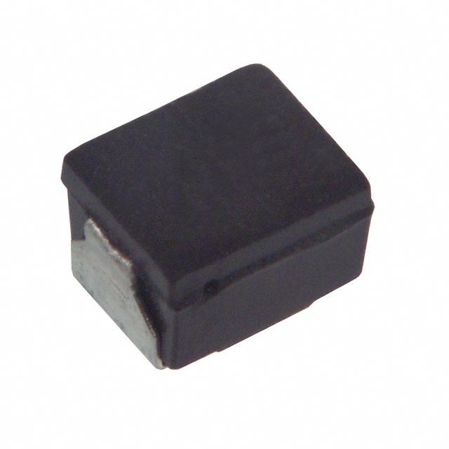
Fixed Inductors (Chip Inductors)
5. Shielded Type SC, SA
Discontinued
■ Features
● Magnetic shield effect using ferrite mixed within outer molding.
● Capable of being Re-flow or flow soldered.
● Good for mounting.
● RoHS compliant
■ Recommended Applications
● AV equipment, Wireless communication equipment and various types of general electronic equipment.
■ Explanation of Part Numbers
1
2
3
4
5
6
7
8
9
10
&
-
+
4
"
�
3
�
,
'
11
Packaging Design No.
Product code
Chip Inductors
Shape
Inductance
SC
2520 (1008)
100
SA
3225 (1210)
470
47 μH
271
270 μH
Size : mm (inch)
10 μH
Inductance tolerance
K
F
Taping
±10 %
■Storage Conditions
● Package
: Normal temperature (–5 to 35 °C), normal humidity (85 %RH max.), shall not be exposed to
direct sunlight and harmful gases and care should be taken so as not to cause dew.
Operating
Temperature
:
–20
to +85 °C
●
■Storage Period
● Solderability may be reduced due to the conditions of high temperature and high humidity which causes the oxidation
of tin-plated terminals. Even if storage conditions are within specified limits, solderability may be reduced with the
passage of time. Therefore, please control the storage conditions and try to use the product within 6 months of receipt.
■Packaging Methods, Soldering Conditions and Safety Precautions
Please see Data Files.
Design and specifications are each subject to change without notice. Ask factory for the current technical specifications before purchase and/or use.
Should a safety concern arise regarding this product, please be sure to contact us immediately.
01 Sep. 2012
1
�Discontinued
Fixed Inductors (Chip Inductors)
■ SC Type 2520 (1008)
● Dimensions in mm (not to scale)
● Recommended Land Pattern in mm (not to scale)
1.2 to 1.6
1.2±0.1
2.0±0.2
Marking
1.4 to 1.5
2.5+0.3
–0.2
1.6±0.2
3.5 to 4.0
0.4±0.2
■ Standard Packing Quantity
● 2000 pcs./Reel
■ Standard Parts
Part No.
(μH)
Inductance
Tolerance Test Freq.
(%)
(MHz)
Q
min.
Test Freq.
(MHz)
SRF ✽1
(MHz) min.
RDC ✽2
(Ω) max.
DC Current
(mA) max.
ELJSC270□F
27
20
4.50
18
ELJSC330□F
33
18
5.20
14
ELJSC390□F
39
15
5.70
13
ELJSC470□F
47
14
6.60
12
ELJSC560□F
56
ELJSC680□F
68
ELJSC820□F
82
ELJSC101□F
100
40
K : ±10 %
2.52
2.52
25
0.796
0.796
13
7.10
10
13
6.50
17
13
7.40
14
12
8.40
10
□ : Symbol of Tolerance ✽1 : Self Resonant Frequency ✽2 : DC Resistance
Design and specifications are each subject to change without notice. Ask factory for the current technical specifications before purchase and/or use.
Should a safety concern arise regarding this product, please be sure to contact us immediately.
01 Sep. 2012
2
�Discontinued
Fixed Inductors (Chip Inductors)
■ SA Type 3225 (1210)
● Dimensions in mm (not to scale)
● Recommended Land Pattern in mm (not to scale)
1.9 to 2.4
1.9±0.1
2.5±0.2
Marking
3.2±0.3
2.2±0.2
1.6 to 2.0
4.0 to 4.6
0.6±0.2
■ Standard Packing Quantity
● 2000 pcs./Reel
■ Standard Parts
Part No.
(μH)
Inductance
Tolerance Test Freq.
(%)
(MHz)
Q
min.
Test Freq.
(MHz)
SRF ✽1
(MHz) min.
RDC ✽2
(Ω) max.
DC Current
(mA) max.
ELJSA100KF
10
30
1.8
18
ELJSA120KF
12
28
2.0
17
ELJSA150KF
15
25
2.2
15
ELJSA180KF
18
23
2.5
13
ELJSA220KF
22
20
2.8
12
ELJSA270KF
27
18
3.2
10
ELJSA330KF
33
17
3.5
10
ELJSA390KF
39
15
3.8
9
ELJSA470KF
47
14
4.0
8
ELJSA560KF
56
13
4.5
7
ELJSA680KF
68
12
5.0
6
ELJSA820KF
82
11
6.0
6
ELJSA101KF
100
10
7.0
5
ELJSA121KF
120
ELJSA151KF
150
ELJSA181KF
180
ELJSA221KF
220
ELJSA271KF
270
5
1
K : ±10 %
40
1.5
0.1
9
8.0
5
5
9.0
5
5
11.0
5
4
12.0
5
4
14.0
5
✽1 : Self Resonant Frequency ✽2 : DC Resistance
Design and specifications are each subject to change without notice. Ask factory for the current technical specifications before purchase and/or use.
Should a safety concern arise regarding this product, please be sure to contact us immediately.
01 Sep. 2012
3
�Fixed Inductors (Chip Inductors)
■ Packaging Methods (Taping)
● Punched Carrier Tape Dimensions in mm (not to scale)
t1
● Type □F
fD0
E
P0
B
F
W
RF, QF, PF
Part
A
P1 P2
t2
RF, QF, PF
Tape running
direction
● Embossed Carrier Tape Dimensions in mm (not to scale)
A
B
W
E
F
P1
0.71
1.21
8.0
1.75
3.5
2.0
P2
P0
0D0
2.0
4.0
01.5
t1
0.7
max.
t2
1.0
max.
E
F
● Type □E, Type ND, Type □C
A
t1
E
f D0
F
1.0
1.8
8.0
1.75
3.5
4.0
ND
1.45
2.25
8.0
1.75
3.5
4.0
NC, FC, PC, LC, SC 2.40
2.90
8.0
1.75
3.5
4.0
P2
P0
0D0
0D1
t1
t2
2.0
4.0
01.5
00.6 (0.27)
B
f D1
P1
P2
P0
Tape running
direction
t2
F
B
Chip component
P1
f D0
t1
P2
P0
Tape running
direction
4.0
01.5
01.0 (0.25) 1.55
4.0
01.5
01.1 (0.25) 1.85
B
W
E
F
P1
3.60
8.0
1.75
3.5
4.0
P2
P0
0D0
t1
t2
2.0
4.0
01.5 (0.25) 2.40
NA, FA, PA, LA,
SA, EA, DA
● Type □B
P2 P0
B
W
F
A
t2
2.0
2.0
E
t2
ND
NC, FC, PC, LC, SC
A
NA, FA, PA, LA,
2.80
SA, EA, DA
W
A
Chip component
1.2
● Type □A
E
f D0
t1
P1
RE, QE, PE
RE, QE, PE
Chip
component
W
W
A
B
Tape running direction
P1
A
B
W
E
F
P1
FB, PB
3.60
4.90
12.0
1.75
5.5
8.0
P2
P0
0D0
t1
t2
FB, PB
2.0
4.0
01.5 (0.30) 3.50
● Taping Reel Dimensions in mm (not to scale)
Parts
Types
E
C
A
B
RF, QF, PF, RE, QE, PE, ND,
180
NC, FC, PC, LC, SC,
NA, FA, PA, LA, SA, EA, DA
D
FB, PB
W
180
B
C
D
E
W
60
13
21
2
9
60
13
21
2
13
A
■ Standard Packing Quantity/Reel
Quantity
Types
RF, QF, PF
RE, QE, PE, ND
NC, FC, PC, LC, SC
NA, FA, PA, LA, SA, EA, DA
FB, PB
Quantity
10000
3000
2000
2000
500
✽ Under conditions of high temperature and humidity
deterioration of the taping and packaging may be
accelerated.
Please carefully control storage conditions and use the
product within 6 months of receipt.
pcs.
pcs.
pcs.
pcs.
pcs.
Design and specifications are each subject to change without notice. Ask factory for the current technical specifications before purchase and/or use.
Should a safety concern arise regarding this product, please be sure to contact us immediately.
03 Sep. 2012
4
�Fixed Inductors (Chip Inductors)
Soldering Conditions
Temperature (°C)
■ Reflow soldering conditions
T3
T2
T1
t2
t1
0
Time
● Pb free solder recommended temperature profile
Preheat
Soldering
Peak Temperature
T1 [°C]
t1 [s]
T2 [°C]
t2 [s]
T3
T3 Limit
Time of
Reflow
□F
150 to 180
60 to 120
230 °C
40 max.
250 °C, 10 s
260 °C, 10 s
2 times max.
□E
150 to 180
60 to 120
230 °C
40 max.
250 °C, 10 s
260 °C, 10 s
2 times max.
□D
150 to 180
60 to 120
230 °C
40 max.
245 °C, 10 s
250 °C, 10 s
2 times max.
□C
150 to 180
60 to 120
230 °C
40 max.
245 °C, 10 s
250 °C, 10 s
2 times max.
□A
150 to 180
60 to 120
230 °C
40 max.
245 °C, 10 s
250 °C, 10 s
2 times max.
□B
150 to 180
60 to 120
230 °C
40 max.
245 °C, 10 s
250 °C, 10 s
2 times max.
Type
■ Flow soldering conditions
Preheat: 130 to 150 °C, 60 to 180 s, Soldering: 260 °C, 5 s max.
■ Notes
● Solderability may be reduced due to the conditions of high temperature and high humidity which causes the oxidation
of tin-plated terminals. Even if storage conditions are within specified limits, solderability may be reduced with the
passage of time. Therefore, please control the storage conditions and try to use the product within 6 months of receipt.
● In case the product has been stored for a period longer than 6 months, use the product only after confirmation of its
solderability.
Design and specifications are each subject to change without notice. Ask factory for the current technical specifications before purchase and/or use.
Should a safety concern arise regarding this product, please be sure to contact us immediately.
03 Sep. 2012
5
�Fixed Inductors (Chip Inductors)
Safety Precautions
(Common precautions for Chip Inductors)
• When using our products, no matter what sort of equipment they might be used for, be sure to make a written
agreement on the specifications with us in advance. The design and specifications in this catalog are subject
to change without prior notice.
• Do not use the products beyond the specifications described in this catalog.
• This catalog explains the quality and performance of the products as individual components. Before use, check
and evaluate their operations when installed in your products.
• Install the following systems for a failsafe design to ensure safety if these products are to be used in equipment
where a defect in these products may cause the loss of human life or other significant damage, such as damage to
vehicles (au to mo bile, train, vessel), traffic lights, medical equipment, aerospace equipment, elec tric heating
appliances, combustion/gas equipment, rotating equipment, and disaster/crime prevention equipment.
✽ Systems equipped with a protection circuit and a protection device
✽ Systems equipped with a redundant circuit or other system to prevent an unsafe status in the event of a single fault
Precautions for use
1. Operation range and environments
1 These products are designed and manufactured for general and stan dard use in general elec tron ic
equipment (e.g. AV equipment, home electric applianc es, office equipment, information and com mu nication
equipment)
2 These products are not intended for use in the following special conditions. Before using the products, carefully check
the effects on their quality and performance, and determine whether or not they can be used.
• In liquid, such as water, oil, chemicals, or organic solvent
• In direct sunlight, outdoors, or in dust
• In salty air or air with a high concentration of corrosive gas, such as Cl2, H2S, NH3, SO2, or NO2
• In an environment where these products cause dew condensation
2. Handling
1 Do not bring magnets or magnetized materials close to the product. The influence of their magnetic field can
change the inductance value.
2 Do not apply strong mechanical shocks by either dropping or collision with other parts.
Excessive schock can damage the part.
3. Land pattern design
1 Please refer to the recommended land pattern for each type shown on the datasheet.
2 Avoid placing the chip inductor on any metal pattern except the recommended land pattern because a drop of Q
and mutual conductance may occur.
3 In case of flow soldering, venting of soldering flux gases should be made for high density assemblies to get a
good solder connection.
4 In case of reflow soldering, consider the layout because taller components close to chip inductor tend to block
thermal conduction.
4. Mounting
1 In general, magnetic and electric characteristics of ferrite cores can be changed by applying excessively strong
force. Placement force should not exceed 20 N.
2 Do not bend or twist the PWB after mounting the part.
5. Cleaning
1 Do not use acid or alkali agents. Some cleaning solvents may damage the part.
Confirm by testing the reliability in advance of mass production.
2 If Ultrasonic cleaning is used, please confirm the reliability in advance.
It is possible that combined resonance of component and PWB and cavitation can cause an abnormal vibration
mode to exist causing damage.
6. Caution about applying excessive current
The rated current is defined as the smaller value of either the current value when the inductance drops 10 %
down from the initial point or the current value when the average temperature of coil inside rises 20 °C up from
the initial point. Do not operate product over the specific max. current.
Package markings include the product number, quantity, and country of origin.
In principle, the country of origin should be indicated in English.
Design and specifications are each subject to change without notice. Ask factory for the current technical specifications before purchase and/or use.
Should a safety concern arise regarding this product, please be sure to contact us immediately.
01 Sep. 2012
6
�Fixed Inductors (Chip Inductors)
Chip Inductors
Type:
Discontinued :Wirewound Chip Inductor. □D, □C, □A, □B
□F, □E, □D, □C, □A, □B
□F
□E
□D
□C
□A
□B
(Size 1005) (Size 1608) (Size 2012) (Size 2520) (Size 3225) (Size 4532)
Ceramic Core/Laser-Cut and wire wound type chip inductors for automatic and high-density mounting
Wide variation product line-up correspond to various needs
■ Recommended Applications
● Cellular phones, wireless communication equipment (W-LAN, Bluetooth), various modules, HIC, TV, VTR, PC & peripherals,
DVD, DSC, STB.
■ Inductors · Selection Guide
Technology
Case
Usage
Size : mm (inch)
Non wound
Wire wound
Discontinued
Size 1005
(0402)
Size 1608
(0603)
Size 2012
(0805)
Size 2520
(1008)
Size 3225
(1210)
Size 4532
(1812)
ELJRF
ELJRE
ELJND
ELJNC
ELJNA
1.0–100 nH
1.0–220 nH
10–1000 nH
10–820 nH
47–8200 nH
ELJQF
ELJQE
1.0–39 nH
2.2–56 nH
ELJFC
ELJFA
ELJFB
0.22–100 µH
0.22–220 µH
0.22–1000 µH
High Freq. Use
High Freq.
High-Q
General Use
ELJPF
ELJPE
ELJPC/PC□3
ELJLC
ELJPA/PA□2
ELJLA
ELJPB
2.2–10 nH
2.2–22 nH
1.0–33 µH
1.0–330 µH
10–220 µH
ELJSC
ELJSA
27–100 µH
10–270 µH
High Power
Magnetically
Shielded
ELJEA
Low DC
Resistance
1.0–330 µH
ELJDA/ELJFA
Signal
Processing Use
(Low Distortion Type)
39–100 µH
Design and specifications are each subject to change without notice. Ask factory for the current technical specifications before purchase and/or use.
Should a safety concern arise regarding this product, please be sure to contact us immediately.
03 Sep. 2012
7
�


 工商网监
湘ICP备2023018690号
工商网监
湘ICP备2023018690号
