Digi-Key
Issue No.
: 151RJ00004103
Date of Issue
: February 6, 2004
Classification
:
New
Change
Renewal
PRODUCT SPECIFICATION FOR INFORMATION
Product Description
:
Thick Film Chip Resistor
Product Part Number
:
ERJ1TYF***U, ERJ1TY0R00U
Classification of Spec
:
Individual Product Spec
Applications
:
Standard electronic equipment
For other applications, contact our person singed below.
Term of Validity
:
February 5, 2009
from the date of issue
CUSTOMER USE ONLY
Receipt Record #
:
Date of Receipt:
:
Received by :
Title :
Dept :
Matsushita Electronic Components Co.,Ltd.
Prepared by : Engineering Department
LCR Device Company
Resistor Business Unit
Contact Person :
H.Yabukoshi
Title :
Approved :
401 Sadamasa-cho, Fukui City, Fukui 910-8502 Japan
Tel : Fukui (0776) 56-8034
Fax : Fukui (0776) 56-3114
S.Hoshitoku
Title : Manager of Engineering
�Spec. No.
Subject
Chip Resistor
PRODUCT SPECIFICATION FOR IMFORMATION
151-SRJ-E7049B
Part No.
ERJ1TYF
14 - 1
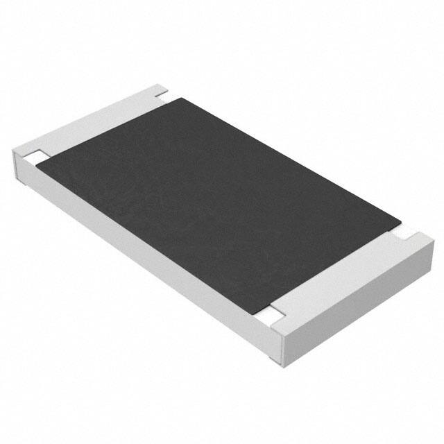
1. Dimension
L
l
a
a
(1) Substrate : Alumina
(2) Protective Coating : Resin
W
(3) Resistive Element : Metal glaze
(4) Inner Termination : Thick film material
(5) Middle Termination : Ni Plating
(1)
(2)
(3)
(4)
(5)
(6)
(6) Outer Termination : Sn Plating
* Under running changing form Sn/Pb plating
t
b
to Sn plating.
b
Dimension (mm)
L
W
a
b
t
l
6.40+/-0.20
3.20+/-0.20
0.65+/-0.20
0.60+/-0.20
0.60+/-0.10
5.10+/-0.20
2. Power Derating Curve
Rated Power (%)
120
70
100
Operating temperature
80
range
60
: -55 to 125 deg.C
40
20
125
0
-60 -40 -20 0 20 40 60 80 100 120 140 160
Ambient Temperature (deg.C)
Figure 1
3. Ratings
3-1 Resistor
Item
Rated value
Explanation
When used at ambient temperature above 70
Power Rating
1.0W
deg.C, power rating shall be determined in
accordance with Figure 1.
MATSUSHITA ELECTRONIC COMPONENTS Co., LTD
�Spec. No.
Subject
Chip Resistor
PRODUCT SPECIFICATION FOR IMFORMATION
151-SRJ-E7049B
Part No.
ERJ1TYF
Item
14 - 2
Rated value
Explanation
The rated voltage of each resistance should be calculated from the equation
Rated voltage &
below. And when the rated voltage exceeds the maximum RCWV,
Rated Continuous
the maximum RCWV should be the rated voltage.
Rated voltage = (Power rating x Resistance Value)
Working Voltage
1/2
The maximum RCWV : 200V
The overload voltage should be 2.5 times the rated voltage. And when
the voltage exceeds the maximum overload voltage, the maximum overload
Overload Voltage
voltage should be the overload voltage.
The maximum overload voltage : 400V
Resistance
F : +/- 1%
Tolerance
Resistance
10 ohm – 1.0 M ohm (E-24 series)
Circuit board of
You should use the aluminum or the ceramic substrate when the added
use
wttage exceeds 0.5W.
3-2 Jumper
Item
Rated value
Explanation
When used at ambient temperature above 70
Ratied current
2 A
deg.C, power rating shall be determined in
accordance with Figure 1.
Overload current
4 A
Resistance value
Less than 50 m ohm
4. Explanation of Part Number
4-1 Resistor
E
R
(1)
J
1
T
(2)
Y
F
(3)
(4)
1
0
(5)
2
U
(6)
(1) Product Code : Thick Film Chip Resistor
(2) Size and Rated Power : 6.4 mm x 3.2mm, 1.0 W
(3) Marking : Marking on Black Side
(4) Resistance Tolerance
Code
Resistance Tolerance
F
+/- 1%
MATSUSHITA ELECTRONIC COMPONENTS Co., LTD
�Spec. No.
Subject
Chip Resistor
PRODUCT SPECIFICATION FOR IMFORMATION
151-SRJ-E7049B
Part No.
ERJ1TYF
14 - 3
(5) Resistance Value
The first two digits are the significant figures of resistance value, and the last figure shows
the number of zero following in ohm.
(6) Packaging Configuration
Code
Packaging Configuration
U
Taping (4000pcs/reel)
4-2 Jumper
E
R
J
1
(1)
T
(2)
Y
0
R
(3)
(4)
0
0
U
(5)
(1) Product Code : Thick Film Chip Resistor
(2) Size and Rated Power : 6.4mm x 3.2 mm
(3) Resistance value
Code
Resistance value
0R00
Jumper (Less than 50 m ohm)
(4) Packaging Configuration
Code
Packaging Configuration
U
Taping (4000pcs/reel)
5. Appearance & Construction
Item
Rated value
Explanation
1. The resistive element should be covered with protective coating that don’t
fade easily. The surface of coating should avoid unevenness, flaw, pinhole
and discoloration.
2. The electrode should be printed uniformly, as shown in the dimensions.
Appearance &
Construction
The plating should not fade easily, and should avoid unevenness, flaw,
pinhole, projection and discoloration.
3. The electrode should be connected electrically, mechanically to resistive
element.
4. Dimensions of the substrate should be as in the list and it should not
have chipping, flaw, flash and crack. Details of appearance criteria shall
be as described in attached sheet.
As far as there shall not designation especially, the following tests and measurement shall be
operated under the following conditions.
Normal temperature : 5 deg.C to 35 deg.C
Normal humidity
: 45 % to 85 %
Normal atmospheric pressure : 86 k Pa to 106 k Pa
MATSUSHITA ELECTRONIC COMPONENTS Co., LTD
�Spec. No.
Subject
Chip Resistor
PRODUCT SPECIFICATION FOR IMFORMATION
151-SRJ-E7049B
Part No.
ERJ1TYF
14 - 4
6. Performance Specification
Item
Specification
Resistor
Jumper
Test Method (JIS-C5201-1)
DC resistance value shall
DC resistance
be within the specified
At 20 deg.C, 65%RH
tolerance.
Natural resistance change per temperature
degree centigrade.
TCR=(R2-R1)x106/R1(t2-t1)
Temperature
coefficient
of resistance
10 ohm – 1 M ohm
R1 : Resistance value at reference
–6
: +/- 200 x 10 /deg.C
(TCR)
(x10–6/deg.C)
temperature (t1)
R2 : Resistance value at test
temperature (t2)
t1 : 25 deg.C , t2 : 125 deg.C
Short time
∆R :
Less than
overload
+/-(2%+0.1ohm)
50m ohm
Resistors shall be applied 2.5 times the rated
voltage for 5 seconds.
Max. overload voltage shall be 400V.
Resistors shall be subjected to 10000 cycles
Intermittent
∆R :
Less than
overload
+/-(5%+0.1ohm)
50m ohm
of 2.5 times the rated voltage applied for 1
second with pause of 25 seconds between
tests.
Max. overload voltage shall be 400V.
AC 400V between substrate and termination
Dielectric
Withstanding
No evidence of flashover,
for 1 minute.
mechanical damage, arcing
AC power
or insulation breakdown
supply
or
Insulation
resistance
Insulation
resistance
meter
Min. 1000 M ohm
Resistors shall be facing down.
After applying DC 400V to the resistor,
insulation resistance shall be measured.
MATSUSHITA ELECTRONIC COMPONENTS Co., LTD
�Spec. No.
Subject
Chip Resistor
PRODUCT SPECIFICATION FOR IMFORMATION
151-SRJ-E7049B
Part No.
ERJ1TYF
Item
14 - 5
Specification
Resistor
Test Method (JIS-C5201-1)
Jumper
10 ohm – 1k ohm
: 0 dB (1.0 µV/V)
1.1k ohm – 9.1k ohm
: 10 dB (3.2 µV/V)
Noise
10k ohm – 91k ohm
: 15 dB (5.6 µV/V)
Noise shall be measured by RESISTOR
NOISE TEST SET MODEL 315C by
Quan-Tech Div.
Max. VR shall be 35 dB.
100k ohm – 910k ohm
: 20 dB (10 µV/V)
7. Machinery characteristic
Item
Specification
Resistor
Jumper
Test Method (JIS-C5201-1)
Cupper plate : t=0.4mm
Pull speed
: 10mm/s
Fixed
Terminal
strength
Solder
Sample
Min. 4.9 N (500g)
P
Copper plate
Substrate : Glass epoxy (t=1.6 mm)
Span : 90mm
Bending distance : 2mm (10 seconds)
No mechanical damage.
Bending
1.85 5.2 1.85
4.0
(mm)
∆R :
Less than
+/-(1%+0.05ohm)
50m ohm
40
strength
100
MATSUSHITA ELECTRONIC COMPONENTS Co., LTD
�Spec. No.
Subject
Chip Resistor
PRODUCT SPECIFICATION FOR IMFORMATION
151-SRJ-E7049B
Part No.
ERJ1TYF
Item
14 - 6
Specification
Resistor
Test Method (JIS-C5201-1)
Jumper
Resistors shall be dipped in the melted solder
Solderability
Termination should be
bath at 235 deg.C +/- 5 deg.C for 2 seconds
covered uniformly with solder
+/- 0.5 second. Flux shall be removed from
(Min. 95% coverage)
the surface of termination with clean organic
solvent.
Resistance to
∆R :
Less than
soldering heat
+/-(1%+0.05ohm)
50m ohm
Resistors shall be dipped in the melted solder
bath at 270 deg.C +/- 3 deg.C for 10 seconds
+/- 1 second.
Resistors shall be subjected to a single
vibration having as double amplitude of 1.5
Resistance to
vibration
(Low frequency)
∆R :
Less than
+/-(1%+0.05ohm)
50m ohm
mm in 3 directions perpendicular one another
for 2 hours each. (6 hours in total)
The vibration frequency shall be varied
uniformly from 10 Hz to 55 Hz, and return
to 10 Hz traversing for 1 min.
Solvent solution : Isopropyl alcohol
Without distinct
Resistance to
solvent
deformation in appearance
∆R :
Less than
+/-(0.5%
+0.05ohm)
50m ohm
(1) Dipping 10 +/- 1 hours, dry in room
condition for 30 +/- 10 minutes.
(2) Ultrasonic wave washing : 5 +/- 1 min.
(0.3W/cm,28kHz)
Dry in room condition for 30 +/-10 minutes.
MATSUSHITA ELECTRONIC COMPONENTS Co., LTD
�Spec. No.
Subject
Chip Resistor
PRODUCT SPECIFICATION FOR IMFORMATION
151-SRJ-E7049B
Part No.
ERJ1TYF
14 - 7
8. Environmental test
Item
Low
temperature
exposure
Low
temperature
Operating
High
temperature
exposure
Specification
Resistor
Jumper
Test Method (JIS-C5201-1)
Resistors shall be exposed at -55 deg.C +/- 3
∆R :
Less than
+/-(1%+0.05ohm)
50m ohm
∆R :
Less than
deg.C for 1.5hours. After applying RCWV for
+/-(1%+0.05ohm)
50m ohm
45 minutes, resistors shall be exposed in room
deg.C with no load for 1000 hours +48/-0
hours.
Resistors shall be placed at –65 deg.C +/- 5
condition for 8 hours +/- 1 hour.
∆R :
Less than
+/-(1%+0.05ohm)
50m ohm
Resistors shall be exposed at 125 deg.C +/- 3
deg.C with no load for 1000 hours +48/-0
hours.
Resistors shall be tested for 5 cycles
continuously in accordance with the following
Temperature
cycling
∆R :
Less than
+/-(1%+0.05ohm)
50m ohm
duty cycle.
Step Temperature (deg.C)
1
-55 +/-3
2
Room temperature
3
+125 +/-3
4
Room temperature
Time (min.)
30
Max. 3
30
Max.3
Resistors shall be exposed at 60 deg.C +/- 2
Humidity
∆R :
Less than
deg.C and 90% to 95% relative hummidity in
(Steady state)
+/-(1%+0.05ohm)
50m ohm
a humidity test chamber for 1000 hours +48/-0
hours.
Salt spray
∆R :
Less than
Spray 5 +/- 1 wt% salt water for 96 +/- 4
+/-(1%+0.05ohm)
50m ohm
hours at 35 +/-2 deg.C.
∆R :
Less than
(1.5 hours "ON", 0.5 hours "OFF") for 1000
+/-(3%+0.1ohm)
50m ohm
hours +48/-0 hours in a test chamber
Resistors shall be operated at DC rated power
Load life
controlled at 70 deg.C +/-2 deg.C.
Resistors shall be operated at DC rated power
Load life in
∆R :
Less than
humidity
+/-(3%+0.1 ohm)
50m ohm
(1.5 hours “ON”, 0.5 hours “OFF”) for 1000
hours +48/-0 hours in a test chamber
controlled at 60 deg.C +/- 2 deg.C and at 90
% to 95% in relative hummidity.
MATSUSHITA ELECTRONIC COMPONENTS Co., LTD
�Spec. No.
Subject
Chip Resistor
PRODUCT SPECIFICATION FOR IMFORMATION
151-SRJ-E7049B
Part No.
ERJ1TYF
Specification
Item
Boiling test
14 - 8
Resistor
Test Method (JIS-C5201-1)
Jumper
∆R :
Less than
+/-(1%+0.05ohm)
50m ohm
Soak in boiling water for 1 +/- 0.1 hour.
Resistors shall be exposed at room condition
for 30 minuites.
9. Other characteristics
Item
Specification
Test method
Resistors shall be mouted on the Ceramic
substrate (t=1.0mm). And the hot spot
Surface
Temperature
temperarure rise of chip resistor shall be
Less than 50 deg.C
measured when applied the rated power.
rise
Applied voltage must not exceed maximun
RCWV.
10. Resistance value Marking
Express resistance value on resin side with three digits.
123 = 12k ohm
123
000 = Chip jumper
The first two digits should be significant figures of
resistance for E-24 series and the third one denotes
number of zeros.
MATSUSHITA ELECTRONIC COMPONENTS Co., LTD
�Spec. No.
Subject
Chip Resistor
PRODUCT SPECIFICATION FOR IMFORMATION
151-SRJ-E7049B
Part No.
ERJ1TYF
14 - 9
11. Common precautions in handling resistors
! Notice for use
(1) This specification shows the quality and performance of a unit component. Before adoption
be sure to evaluate and verify the product mounting it in your product.
(2) We take no responsibility for troubles caused by the product usage that is not specified in
this catalog. Be sure to exchange the delivery specification with us.
(3) Use fail-safe design and ensure safety by carrying out the following items in cases where it
is forecast that the failure of the product gives serious damage to something important like
human life, for instant in traffic transportation equipment (trains, cars, traffic signal
equipment, etc.), medical equipment, aerospace equipment, electric heating appliances,
combustion and gas equipment, rotating equipment, disaster and crime preventive
equipment.
*Ensure safety as the system by setting protective circuits and protective equipment.
*Ensure safety as the system by setting such redundant circuits as do not cause danger by
a single failure.
(4) When a dogma shall be occurred about safety for this product, be sure to inform us rapidly,
operate your technical examination.
(5) The product is designed to use in general standard applications of general electric
equipment (AV products, household electric appliances, office equipment, information and
communication equipment, etc.); hence, it do not take the use under the following special
environments into consideration.
Accordingly, the use in the following special environments, and such environmental
conditions may affect the performance of the product; prior to use, verify the performance,
reliability, etc. thoroughly.
1) Use in liquids such as water, oil, chemical, and organic solvent.
2) Use under direct sunlight, in outdoor or in dusty atmospheres.
3) Use in places full of corrosive gases such as sea breeze, Cl2, H2S, NH3, SO2, and NOX.
4) Use in environment with large static electricity or strong electromagnetic waves.
5) Where the product is close to a heating component, and where an inflammable such as
a polyvinyl chloride wire is arranged close to the product.
6) Where the resistor is sealed or coated with resin, etc.
7) Where water or a water-soluble detergent is used in cleaning free soldering and in flux
cleaning after soldering (Pay particular attention to soluble flux.)
(6) If transient load (heavy load in a short time) like pulse is expected to be applied, carry out
evaluation and confirmation test with resistors actually mounted on your own board. When
the load of more than rated power is applied under the load condition at steady state, it
may impair performance and/or reliability of resistor. Never exceed the rated power. When
MATSUSHITA ELECTRONIC COMPONENTS Co., LTD
�Spec. No.
Subject
Chip Resistor
PRODUCT SPECIFICATION FOR IMFORMATION
151-SRJ-E7049B
Part No.
ERJ1TYF
14 - 10
the product shall be used under special condition, be sure to ask us in advance.
(7) Halogen type (Chlorine type, Bromine type, etc.) or other high-activity flux is not
recommended as the residue may affect performance or reliability of resistors.
(8) When soldering with soldering iron, never touch the body of the chip resistor with a tip of
the soldering iron. When using a soldering iron with a tip at high temperature, solder for a
time as short as possible. (three seconds or less up to 350 deg.C)
(9) Avoid physical shock to the resistor and nipping of the resistor with hard tool (a pair of
pliers or tweezers) as it may damage protective film or the body of resistor and may affect
resistor’s performance.
(10) Avoid immersion of chip resistor in solvent for long time. Use solvent after the effect of
immersion is confirmed.
12. Storage Method
If the product is stored in the following environments and conditions, the performance and
solderability may be badly affected, avoid the storage in the following environments.
(1) Storage in places full of corrosive gases such as sea breeze, Cl2, H2S, NH3, SO2, and NOX.
(2) Storage in places exposed to direct sunlight.
(3) Storage in places outside the temperature range of 5 deg.C to 35 deg.C and humidity
range of 45 %RH to 85 %RH.
(4) The period of guarantee for performance such as solderability is 1 year after our delivery; and
this condition applies only to the case where the storage method specified in item 3) has been
followed.
13. Laws and Regulations
(1) This product has not been manufactured with any ozone-depleting chemical controlled under
the Montreal Protocol.
(2) All materials used in this part are registered material under the Law Concerning the
Examination and Regulation of Manufacturs, etc. of Chemical substances.
(3) All the materials used in this part contain no brominated materials of PBBOS or PBBS as the
flame-retardant.
(4) If you need the notice by letter of “A preliminary judgement on the Laws of Japan foreign
exchange and Foreign Trade control”, be sure to let us know.
MATSUSHITA ELECTRONIC COMPONENTS Co., LTD
�Spec. No.
Subject
Chip Resistor
PRODUCT SPECIFICATION FOR IMFORMATION
151-SRJ-E7049B
Part No.
ERJ1TYF
14 - 11
14. Receipt and Valid time limit for Product Specification for Information
(1) Be sure to return a copy to our company after stamping your company acceptance.
If you shall not return a copy by 3 months which a valid time limit of listing shall expire, we
judge that you shall receive this specification.
(2) By 3 months that a valid time limit of listing shall expire, if there shall not offering it by letter,
a valid time limit shall continue every 1 year.
If an alteration shall be done on the way futher more, a former specification shall become
invalid.
15. Production site
* Country : Japan
Plant : Fukui Matsushita Electric Co.,Ltd.
* Country : Malaysia
Plant : Matsushita Electronic Device (M) Sdn. Bhd.
* Country : China
Plant : Tianjin Matsushita Electronic Components Co.,Ltd.
MATSUSHITA ELECTRONIC COMPONENTS Co., LTD
�Spec. No.
Subject
Chip Resistor
PRODUCT SPECIFICATION FOR IMFORMATION
151-SRJ-E7049B
Part No.
ERJ1TYF
14 - 12
16. Taped and Reel Package
16-1 Physical Dimensions
Structure and reel dimensions shall be as shown in the figure below.
15.4 +/- 1.0
13.0 +/- 1.0
180.0 +0 / -3.0
Min. 60.0
Min. 60.0
Top tape
13.0 +/- 1.0
Carrier tape
Adhesive tape
16-2 Carrier tape dimension
T
P1
P2
Sprocket hole
E
P0
øD0
F
W
B
ØD1
Chip hole
T2
A
Dimension (mm) 3.60+/-0.20
P2
Dimension (mm) 2.00+/-0.05
Unit : mm
Chip resistor
A
B
W
F
E
P1
6.90+/-0.20
12.0+/-0.30
5.50+/-0.05
1.75+/-0.10
4.00+/-0.10
P0
øD0
T
øD1
T2
Max. 0.40
Min. 1.50
1.10+/-0.10
4.00+/-0.10 1.50+0.10/-0
16-3 Specifications
16-3-1 Taping
(1) Minimum Bending Radius
When Carrier tape shall be bent by Minimum Bending Radius (15mm), no defection of chip
and no break of carrier tape. However minimum bending radius shall be tested for 1 time.
(2) Resistance to climate
When resistors shall be exposed at 60 deg.C, 90 to 95 %RH for 120 hours, no defection of
chip and no break of carrier tape.
When the top tape shall be peeled tape should not have flash and tear.
MATSUSHITA ELECTRONIC COMPONENTS Co., LTD
�Spec. No.
Subject
Chip Resistor
PRODUCT SPECIFICATION FOR IMFORMATION
151-SRJ-E7049B
Part No.
ERJ1TYF
14 - 13
(3) When the test shall be operated with the below conditions, peel strength should be 0.098 N
to 0.686 N (10 to 70 g), should not have flash and tear after peeling.
(Test Method)
Carrier tape
Peeling direction
10 degree
Top tape
16-3-2 Quantity in Taping : 4000 pcs./reel
16-3-3 Tape packaging
(1) Resistance side shall be facing upward.
(2) Chip resistor array shall not be sticking to top tape and bottom tape.
(3) Chip resistor array shall be easy to take out from carrier tape and chip hole or sprocket
hole shall not have flash and break.
16-4 Outer Packaging
Quantity : 15 reels (Max. 60,000pcs.)
Tape
Marking
* When taping shall not reach Max. or quantity, the remaining empty space shall be buried with
buffer material.
* When the quantity shall be few, alternative packaging methods may be used. No problem must
occur during the exportation of the product.
16-5 Marking
At last, production country is displayed in English.
(1) Side of reel (Marking shall be on one side)
1) Part name, 2)Part number, 3)Quantity, 4)Lot number, 5)Maker name
6) Poduction country
(2)Packaging box
1)Customer name, 2)Part name, 3)Part number, 4)Customer part number, 5)Quantity
6)Maker name, 7)Poduction country
MATSUSHITA ELECTRONIC COMPONENTS Co., LTD
�Spec. No.
Subject
Chip Resistor
PRODUCT SPECIFICATION FOR IMFORMATION
151-SRJ-E7049B
Part No.
ERJ1TYF
14 - 14
17. Appearance Quality Criteria
Item
Appearance quality
criteria
Figure
A
Protective coating
Chipping
W
A≤W/4
B≤C/2
B
C
Remark
Chipping on both
sides shall be
considered defective
B
Terminal
Chipping
A≤W/4
A
W
B≤Terminal width
One pin hole /
chip resistor
φ
Pin hole
φ ≤ 0.2 mm
Pin hole penetrates
The resistive material.
A
Flash
A≤0.1 mm
A
Top terminal
Lacking
A
W
A≤W/4
A
Side terminal
Lacking
A≤W/4
W
Protective coating
and terminal
aberration
Protective coating and terminal aberration
shall be within the terminal width dimension
Marking
Marking must be readable.
MATSUSHITA ELECTRONIC COMPONENTS Co., LTD
�