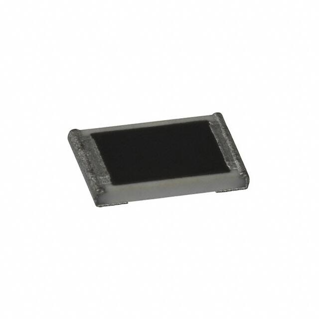
Precision Thick Film Chip Resistors
ERJ type
ERJ XG, 1G series
ERJ 1R, 2R, 3R, 6R series
ERJ 3E, 6E, 8E, 14, 12, 1T series
(Oct. 2021) Products marked as “NRFND” are
not recommended for new design.
Target products : ERJ8E, 14, 12, 1Tseries
Please refer to the recommended alternatives with
”Design Support Tool” ・
Features
● Small size and lightweight
: Metal glaze thick film resistive element and three layers of electrodes
● High reliability
: Taping packaging available
● Compatible with placement machines
● Suitable for both reflow and flow soldering
: ERJXG, 1G, 2R, 3E, 6E, 8E, 14, 12, 1T series :±1 %
● Low resistance tolerance
ERJ1R, 2R, 3R, 6R series
:±0.5 %
: IEC 60115-8,JIS C 5201-8,JEITA RC-2134C
● Reference standard
● AEC-Q200 compliant (except ERJXG, ERJ1R)
● RoHS compliant
■ As for packaging methods, land pattern, soldering conditions and safety precautions,
please see data files.
Explanation of part numbers
● ERJ1R, 2R, 3R, 6R series : ±0.5 %
1
2
3
4
5
6
7
8
9
10
E
R
J
3
R
B
D
1
0
0
Product code
Size, Power rating
Thick film
chip resistors
Code inch Power rating
T.C.R.,Marking
T.C.R.
Code
D
0201
0.05 W
H
±50 ×10–6/K (1R, 2R)
2R
0402
0.063 W
B
±50 ×10–6/K (3R, 6R)
3R
0603
0.1 W
K
±100 ×10–6/K (2R)
6R
0805
0.1 W
E
±100 ×10–6/K (3R, 6R)
12
V
2
Packaging methods
Resistance tolerance
Code
1R
11
Tolerance
±0.5 %
Resistance value
Code
Packaging
Part No.
C
Pressed carrier taping
2 mm pitch, 15,000 pcs
ERJ1R
X
Punched carrier taping
2 mm pitch, 10,000 pcs
ERJ2R
V
Punched carrier taping
4 mm pitch, 5,000 pcs
ERJ3R
ERJ6R
The first three digits are significant
figures of resistance and the last one
denotes number of zeros following.
Example : 1002 → 10 KΩ
Design and specifications are each subject to change without notice. Ask factory for the current technical specifications before purchase and/or use.
Should a safety concern arise regarding this product, please be sure to contact us immediately.
2-Nov-21
�Precision Thick Film Chip Resistors
Explanation of part numbers
● ERJXGN, 1GN, 2RC, 2RK, 3EK, 6EN, 8EN, 14N, 12N, 12S, 1TN series : ±1 %
1
2
3
4
5
6
7
8
9
10
E
R
J
8
E
N
F
1
0
0
Product code
Size, Power rating
Thick film
chip resistors
Resistance tolerance
Code
inch
Power rating
Code
XGN
01005
0.031 W
F
1GN
0201
0.05 W
2RC
0402 0.1 W
2RK
0402 0.1 W
3EK
0603 0.1 W
6EN
0805
0.125 W
NRFND
8EN
1206
0.25 W
NRFND
14N
1210 0.5 W
NRFND
12N
1812
0.75 W
NRFND
12S
2010
0.75 W
NRFND
1TN
2512
1W
V
2
Resistance value
Packaging methods
Tolerance
±1 %
12
11
The first three digits are significant
figures of resistance and the last
one denotes number of zeros
following.
Decimal point is expressed by "R".
Example : 1002 → 10 kΩ
Code
Packaging
Part No.
Y
Pressed carrier taping
W8P2, 20,000 pcs
U
Embossed carrier taping
W4P1, 40,000 pcs
C
Pressed carrier taping
2 mm pitch, 15,000 pcs
X
Punched carrier taping
2 mm pitch, 10,000 pcs
V
Punched carrier taping
4 mm pitch, 5,000 pcs
ERJXGN
ERJ1GN
ERJ2RC
ERJ2RK
ERJ3EK
ERJ6EN
ERJ8EN
NRFND
NRFND
U
NRFND
Embossed carrier taping
4 mm pitch, 5,000 pcs
ERJ14N
ERJ12N
ERJ12S
Embossed carrier taping
4 mm pitch, 4,000 pcs
ERJ1TN
Not recommended for new design
Ratings
<±0.5 %>
Part No.
(inch size)
Rated power*1
(70 ℃)
(W)
Limiting
element
voltage*2
(V)
Maximum
overload
voltage*3
(V)
0.05
15
30
±0.5
1 k to 1 M
0.063
50
100
±0.5
100 to 100 k
0.063
50
100
±0.5
0.1
75*4
150*4
±0.5
0.1
75
*4
*4
0.1
150
200
±0.5
0.1
150
200
±0.5
ERJ1RH
(0201)
ERJ2RH
(0402)
ERJ2RK
(0402)
ERJ3RB
(0603)
ERJ3RE
(0603)
ERJ6RB
(0805)
ERJ6RE
(0805)
150
Resistance
tolerance
(%)
±0.5
T.C.R.
(×10-6/K)
Category
temperature
range
(℃)
AEC-Q200
Grade
(E24,E96)
±50
-55 to +125
-
(E24,E96)
±50
(E24,E96)
±100
(E24,E96)
±50
-55 to +155
Grade 0
Resistance
range
(Ω)
10 to 97.6
102 k to 1 M
100 to 100 k
10 to 97.6
102 k to 1 M
100 to 100 k
10 to 97.6
102 k to 1 M
(E24,E96)
±100
(E24,E96)
±50
(E24,E96)
±100
*1 : Use it on the condition that the case temperature is below the upper category temperature.
*2 : Rated continuous working voltage (RCWV) shall be determined from RCWV=√Power rating × Resistance value,
or limiting element voltage listed above, whichever less.
*3 : Overload test voltage (OTV) shall be determined from OTV = specified magnification (refer to performance) × RCWV
or maximum overload voltage listed above, whichever less.
*4 : UPGRADE
Design and specifications are each subject to change without notice. Ask factory for the current technical specifications before purchase and/or use.
Should a safety concern arise regarding this product, please be sure to contact us immediately.
2-Nov-21
�Precision Thick Film Chip Resistors
Ratings
