Multilayer NTC Thermistors
ERTJ series
Features
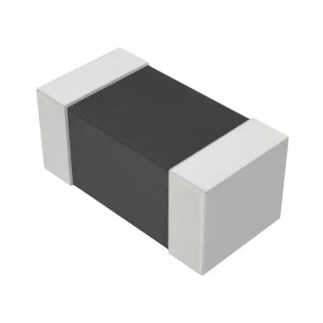
●Surface Mount Device (0201・0402・0603)
●Highly reliable multilayer / monolithic structure
●Wide temperature operating range (-40 to 125 ℃)
●Environmentally-friendly lead-free
●RoHS compliant
Recommended applications
●Mobile Phone
・Temperature compensation for crystal oscillator
・Temperature compensation for semiconductor devices
●Personal Computer and Peripheral Device
・Temperature detection for CPU and memory device
・Temperature compensation for ink-viscosity (Inkjet Printer)
●Battery Pack (secondary battery)
・Temperature detection of battery cells
●Liquid Crystal Display
・Temperature compensation of display contrast
・Temperature compensation of display backlighting (CCFL)
Explanation of part numbers
1
2
3
4
5
6
7
8
9
10
E
R
T
J
0
E
G
1
0
3
Common code
Type code
Product code
ERT
NTC
Thermistors
J
Chip type
(SMD)
Multilayer
type
Size code
(inch size)
Z
0201
0
0402
1
0603
B Value class code
Packaging
style code
0201,0402
Pressed carrier
E taping punched
carrier taping
(Pitch : 2 mm)
V
0603
Punched carrier
taping
(Pitch : 4 mm)
11
J
Nominal resistance
A
2701 to 2800
R25 (Ω)
G
3301 to 3400
M
3801 to 3900
The first two digits are
significant figures of
resistance and the
third one denotes the
number of zeros
following them.
P
4001 to 4100
R
4201 to 4300
S
4301 to 4400
T
4401 to 4500
V
4601 to 4700
12
A
Example
Resistance tolerance
code
Special
specification
F ±1 % Narrow
tolerance
G ±2 % type
H ±3 % Standard
J ±5 % type
Construction
③
④
➄
①
②
No.
Name
①
Semiconductive ceramics
②
Internal electrode
③
④
Substrate electrode
Terminal electrode
➄
Design and specifications are each subject to change without notice. Ask factory for the current technical specifications before purchase and/or use.
Should a safety concern arise regarding this product, please be sure to contact us immediately.
Intermediate electrode
External electrode
1-Mar-20
�Multilayer NTC Thermistors
Ratings
Size code (inch size)
Z(0201)
0(0402)
Operating temperature range
Rated maximum power dissipation*1
Dissipation factor
*2
1(0603)
–40 to 125 ℃
33 mW
66 mW
100 mW
Approximately 1 mW / ℃
Approximately 2 mW / ℃
Approximately 3 mW / ℃
*1: Rated Maximum Power Dissipation : The maximum power that can be continuously applied at the rated ambient temperature.
・The maximum value of power, and rated power is same under the condition of ambient temperature 25 ℃ or less. If the temperature
exceeds 25 ℃, rated power depends on the decreased power dissipation curve.
・Please see “Operating Power” for details.
*2: Dissipation factor : The constant amount power required to raise the temperature of the Thermistor 1 ℃ through self heat generation
under stable temperatures.
・Dissipation factor is the reference value when mounted on a glass epoxy board (1.6 mmT).
Part number list of narrow tolerance type (Resistance tolerance : ±2 %, ±1 %)
● 0201 inch size
Part number
ERTJZEG103□A
ERTJZEP473□
ERTJZEP683□
ERTJZER683□
ERTJZER104□
ERTJZET104□
ERTJZEV104□
Nominal resistance
at 25 ℃ (Ω)
10 kΩ
47 kΩ
68 kΩ
68 kΩ
100 kΩ
100 kΩ
100 kΩ
Resistance tolerance
B Value
at 25/50 (K)
B Value
at 25/85 (K)
±1 %(F)
or
±2 %(G)
(3380 K)
4050 K±1 %
4050 K±1 %
4250 K±1 %
4250 K±1 %
4500 K±1 %
4700 K±1 %
3435 K±1 %
(4100 K)
(4100 K)
(4300 K)
(4300 K)
(4550 K)
(4750 K)
Resistance tolerance
B Value
at 25/50 (K)
B Value
at 25/85 (K)
±1 %(F)
or
±2 %(G)
(3380 K)
4050 K±1 %
4050 K±1 %
4050 K±1 %
4250 K±1 %
4330 K±1 %
4700 K±1 %
4700 K±1 %
3435 K±1 %
(4100 K)
(4100 K)
(4100 K)
(4300 K)
(4390 K)
(4750 K)
(4750 K)
Resistance tolerance
B Value
at 25/50 (K)
B Value
at 25/85 (K)
±1 %(F)
or ±2 %(G)
(3380 K)
(4330 K)
3435 K±1 %
4390 K±1 %
● 0402 inch size
Part number
ERTJ0EG103□A
ERTJ0EP333□
ERTJ0EP473□
ERTJ0EP683□
ERTJ0ER104□
ERTJ0ES104□
ERTJ0EV104□
ERTJ0EV224□
Nominal resistance
at 25 ℃ (Ω)
10 kΩ
33 kΩ
47 kΩ
68 kΩ
100 kΩ
100 kΩ
100 kΩ
220 kΩ
● 0603 inch size
Part number
ERTJ1VG103□A
ERTJ1VS104□A
Nominal resistance
at 25 ℃ (Ω)
10 kΩ
100 kΩ
□ : Resistance tolerance code
Part number list of standard type (Resistance tolerance : ±5 %, ±3 %)
● 0201 inch size
Part number
ERTJZET202□
ERTJZET302□
ERTJZET472□
ERTJZEG103□A
ERTJZEP473□
ERTJZEP683□
ERTJZER683□
ERTJZER104□
ERTJZET104□
ERTJZEV104□
ERTJZET154□
ERTJZET224□
Nominal resistance
at 25 ℃ (Ω)
2.0 kΩ
3.0 kΩ
4.7 kΩ
10 kΩ
47 kΩ
68 kΩ
68 kΩ
100 kΩ
100 kΩ
100 kΩ
150 kΩ
220 kΩ
Resistance tolerance
B Value
at 25/50 (K)
B Value
at 25/85 (K)
±3 %(H)
or
±5 %(J)
4500 K±2 %
4500 K±2 %
4500 K±2 %
(3380 K)
4050 K±2 %
4050 K±2 %
4250 K±2 %
4250 K±2 %
4500 K±2 %
4700 K±2 %
4500 K±2 %
4500 K±2 %
(4450 K)
(4450 K)
(4450 K)
3435 K±1 %
(4100 K)
(4100 K)
(4300 K)
(4300 K)
(4550 K)
(4750 K)
(4750 K)
(4750 K)
□ : Resistance tolerance code
Design and specifications are each subject to change without notice. Ask factory for the current technical specifications before purchase and/or use.
Should a safety concern arise regarding this product, please be sure to contact us immediately.
1-Mar-20
�Multilayer NTC Thermistors
Part number list of standard type (Resistance tolerance : ±5 %, ±3 %)
● 0402 inch size
Part number
Nominal resistance
at 25 ℃ (Ω)
Resistance tolerance
B Value
at 25/50 (K)
B Value
at 25/85 (K)
ERTJ0EA220□
22 Ω
2750 K±3 %
(2700 K)
ERTJ0EA330□
33 Ω
2750 K±3 %
(2700 K)
ERTJ0EA400□
40 Ω
2750 K±3 %
(2700 K)
ERTJ0EA470□
47 Ω
2750 K±3 %
(2700 K)
ERTJ0EA680□
68 Ω
2800 K±3 %
(2750 K)
ERTJ0EA101□
100 Ω
2800 K±3 %
(2750 K)
ERTJ0EA151□
150 Ω
2800 K±3 %
(2750 K)
ERTJ0ET102□
1.0 kΩ
4500 K±2 %
(4450 K)
ERTJ0ET152□
1.5 kΩ
4500 K±2 %
(4450 K)
ERTJ0ET202□
2.0 kΩ
4500 K±2 %
(4450 K)
ERTJ0ET222□
2.2 kΩ
4500 K±2 %
(4450 K)
ERTJ0ET302□
3.0 kΩ
4500 K±2 %
(4450 K)
ERTJ0ER332□
3.3 kΩ
4250 K±2 %
(4300 K)
ERTJ0ET332□
3.3 kΩ
4500 K±2 %
(4450 K)
ERTJ0ET472□
4.7 kΩ
4500 K±2 %
(4450 K)
ERTJ0ER472□
4.7 kΩ
4250 K±2 %
(4300 K)
ERTJ0ER682□
6.8 kΩ
4250 K±2 %
(4300 K)
ERTJ0EG103□A
10 kΩ
(3380 K)
3435 K±1 %
ERTJ0EM103□
10 kΩ
3900 K±2 %
(3970 K)
ERTJ0ER103□
10 kΩ
4250 K±2 %
(4300 K)
ERTJ0ER153□
15 kΩ
4250 K±2 %
(4300 K)
ERTJ0ER223□
22 kΩ
4250 K±2 %
(4300 K)
ERTJ0EP333□
33 kΩ
4050 K±2 %
(4100 K)
ERTJ0ER333□
33 kΩ
4250 K±2 %
(4300 K)
ERTJ0ET333□
33 kΩ
4500 K±2 %
(4580 K)
ERTJ0EP473□
47 kΩ
4050 K±2 %
(4100 K)
ERTJ0ET473□
47 kΩ
4500 K±2 %
(4550 K)
ERTJ0EV473□
47 kΩ
4700 K±2 %
(4750 K)
ERTJ0EP683□
68 kΩ
4050 K±2 %
(4100 K)
ERTJ0ER683□
68 kΩ
4250 K±2 %
(4300 K)
ERTJ0EV683□
68 kΩ
4700 K±2 %
(4750 K)
ERTJ0EP104□
100 kΩ
4050 K±2 %
(4100 K)
ERTJ0ER104□
100 kΩ
4250 K±2 %
(4300 K)
ERTJ0ES104□
100 kΩ
4330 K±2 %
(4390 K)
ERTJ0ET104□
100 kΩ
4500 K±2 %
(4580 K)
ERTJ0EV104□
100 kΩ
4700 K±2 %
(4750 K)
ERTJ0ET154□
150 kΩ
4500 K±2 %
(4580 K)
ERTJ0EV154□
150 kΩ
4700 K±2 %
(4750 K)
ERTJ0EV224□
220 kΩ
4700 K±2 %
(4750 K)
ERTJ0EV334□
330 kΩ
4700 K±2 %
(4750 K)
ERTJ0EV474□
470 kΩ
4700 K±2 %
(4750 K)
±3 %(H)
or
±5 %(J)
□ : Resistance tolerance code
Design and specifications are each subject to change without notice. Ask factory for the current technical specifications before purchase and/or use.
Should a safety concern arise regarding this product, please be sure to contact us immediately.
1-Mar-20
�Multilayer NTC Thermistors
Part number list of standard type (Resistance tolerance : ±5 %, ±3 %)
● 0603 inch size
Part number
Nominal resistance
at 25 ℃ (Ω)
Resistance tolerance
B Value
at 25/50 (K)
B Value
at 25/85 (K)
ERTJ1VA220□
22 Ω
2750 K±3 %
(2700 K)
ERTJ1VA330□
33 Ω
2750 K±3 %
(2700 K)
ERTJ1VA400□
40 Ω
2800 K±3 %
(2750 K)
ERTJ1VA470□
47 Ω
2800 K±3 %
(2750 K)
ERTJ1VA680□
68 Ω
2800 K±3 %
(2750 K)
ERTJ1VA101□
100 Ω
2800 K±3 %
(2750 K)
ERTJ1VT102□
1.0 kΩ
4500 K±2 %
(4450 K)
ERTJ1VT152□
1.5 kΩ
4500 K±2 %
(4450 K)
ERTJ1VT202□
2.0 kΩ
4500 K±2 %
(4450 K)
ERTJ1VT222□
2.2 kΩ
4500 K±2 %
(4450 K)
ERTJ1VT302□
3.0 kΩ
4500 K±2 %
(4450 K)
ERTJ1VT332□
3.3 kΩ
4500 K±2 %
(4450 K)
ERTJ1VR332□
3.3 kΩ
4250 K±2 %
(4300 K)
ERTJ1VR472□
4.7 kΩ
4250 K±2 %
(4300 K)
ERTJ1VT472□
4.7 kΩ
4500 K±2 %
(4450 K)
ERTJ1VR682□
6.8 kΩ
4250 K±2 %
(4300 K)
ERTJ1VG103□A
10 kΩ
(3380 K)
3435 K±1 %
ERTJ1VR103□
10 kΩ
4250 K±2 %
(4300 K)
ERTJ1VR153□
15 kΩ
4250 K±2 %
(4300 K)
ERTJ1VR223□
22 kΩ
4250 K±2 %
(4300 K)
ERTJ1VR333□
33 kΩ
4250 K±2 %
(4300 K)
ERTJ1VP473□
47 kΩ
4100 K±2 %
(4150 K)
ERTJ1VR473□
47 kΩ
4250 K±2 %
(4300 K)
ERTJ1VV473□
47 kΩ
4700 K±2 %
(4750 K)
ERTJ1VR683□
68 kΩ
4250 K±2 %
(4300 K)
ERTJ1VV683□
68 kΩ
4700 K±2 %
(4750 K)
ERTJ1VS104□A
100 kΩ
(4330 K)
4390 K±1 %
ERTJ1VV104□
100 kΩ
4700 K±2 %
(4750 K)
ERTJ1VV154□
150 kΩ
4700 K±2 %
(4750 K)
ERTJ1VT224□
220 kΩ
4500 K±2 %
(4580 K)
±3 %(H)
or
±5 %(J)
□ : Resistance tolerance code
Design and specifications are each subject to change without notice. Ask factory for the current technical specifications before purchase and/or use.
Should a safety concern arise regarding this product, please be sure to contact us immediately.
1-Mar-20
�Multilayer NTC Thermistors
Part number list of standard type (Resistance tolerance : ±5 %, ±3 %)
● Temperature and Resistance value (the resistance value at 25 ℃ is set to 1)/ Reference values
ERTJ□□A to
ERTJ□□G to ERTJ□□M to
ERTJ□□P to
ERTJ□□R to
ERTJ0ES to
ERTJ1VS to
ERTJ□□T to
ERTJ□□T to
ERTJ□□V to
B25/50
2750 K
2800 K
(3375 K)
3900 K
4050 K
4250 K
4330 K
(4330 K)
4500 K
4500 K
4700 K
B25/85
(2700 K)
(2750 K)
3435 K
(3970 K)
(4100 K)
(4300 K)
(4390 K)
4390 K
(4450 K)
(4580 K)
(4750 K)
*1
*2
T(℃)
13.28
20.52
32.11
33.10
43.10
45.67
45.53
63.30
47.07
59.76
10.21
10.40
15.48
23.29
24.03
30.45
32.08
31.99
42.92
33.31
41.10
8.061
8.214
11.79
17.08
17.63
21.76
22.80
22.74
29.50
23.80
28.61
-25
6.427
6.547
9.069
12.65
13.06
15.73
16.39
16.35
20.53
17.16
20.14
-20
5.168
5.261
7.037
9.465
9.761
11.48
11.91
11.89
14.46
12.49
14.33
-15
4.191
4.261
5.507
7.147
7.362
8.466
8.743
8.727
10.30
9.159
10.31
-10
3.424
3.476
4.344
5.444
5.599
6.300
6.479
6.469
7.407
6.772
7.482
-5
2.819
2.856
3.453
4.181
4.291
4.730
4.845
4.839
5.388
5.046
5.481
0
2.336
2.362
2.764
3.237
3.312
3.582
3.654
3.650
3.966
3.789
4.050
5
1.948
1.966
2.227
2.524
2.574
2.734
2.778
2.776
2.953
2.864
3.015
10
1.635
1.646
1.806
1.981
2.013
2.102
2.128
2.126
2.221
2.179
2.262
15
1.38
1.386
1.474
1.567
1.584
1.629
1.642
1.641
1.687
1.669
1.710
20
1.171
1.174
1.211
1.247
1.255
1.272
1.277
1.276
1.293
1.287
1.303
-40
13.05
-35
-30
25
1
1
1
1
1
1
1
1
1
1
1
30
0.8585
0.8565
0.8309
0.8072
0.8016
0.7921
0.7888
0.7890
0.7799
0.7823
0.7734
35
0.7407
0.7372
0.6941
0.6556
0.6461
0.6315
0.6263
0.6266
0.6131
0.6158
0.6023
40
0.6422
0.6376
0.5828
0.5356
0.5235
0.5067
0.5004
0.5007
0.4856
0.4876
0.4721
45
0.5595
0.5541
0.4916
0.4401
0.4266
0.4090
0.4022
0.4025
0.3874
0.3884
0.3723
50
0.4899
0.4836
0.4165
0.3635
0.3496
0.3319
0.3251
0.3254
0.3111
0.3111
0.2954
55
0.4309
0.4238
0.3543
0.3018
0.2881
0.2709
0.2642
0.2645
0.2513
0.2504
0.2356
60
0.3806
0.3730
0.3027
0.2518
0.2386
0.2222
0.2158
0.2161
0.2042
0.2026
0.1889
65
0.3376
0.3295
0.2595
0.2111
0.1985
0.1832
0.1772
0.1774
0.1670
0.1648
0.1523
70
0.3008
0.2922
0.2233
0.1777
0.1659
0.1518
0.1463
0.1465
0.1377
0.1348
0.1236
75
0.2691
0.2600
0.1929
0.1504
0.1393
0.1264
0.1213
0.1215
0.1144
0.1108
0.1009
80
0.2417
0.2322
0.1672
0.1278
0.1174
0.1057
0.1011
0.1013
0.09560
0.09162
0.08284
85
0.2180
0.2081
0.1451
0.1090
0.09937
0.08873
0.08469
0.08486
0.08033
0.07609
0.06834
90
0.1974
0.1871
0.1261
0.09310
0.08442
0.07468
0.07122
0.07138
0.06782
0.06345
0.05662
95
0.1793
0.1688
0.1097
0.07980
0.07200
0.06307
0.06014
0.06028
0.05753
0.05314
0.04712
100
0.1636
0.1528
0.09563
0.06871
0.06166
0.05353
0.05099
0.05112
0.04903
0.04472
0.03939
105
0.1498
0.1387
0.08357
0.05947
0.05306
0.04568
0.04340
0.04351
0.04198
0.03784
0.03308
110
0.1377
0.1263
0.07317
0.05170
0.04587
0.03918
0.03708
0.03718
0.03609
0.03218
0.02791
115
0.1270
0.1153
0.06421
0.04512
0.03979
0.03374
0.03179
0.03188
0.03117
0.02748
0.02364
120
0.1175
0.1056
0.0565
0.03951
0.03460
0.02916
0.02734
0.02742
0.02702
0.02352
0.02009
125
0.1091
0.09695
0.04986
0.03470
0.03013
0.02527
0.02359
0.02367
0.02351
0.02017
0.01712
*1: Apply to products with a B25/50 constant of 4500 K and a resistance value of 25 ℃ less than 10 kΩ.
*2: Apply to products with a B25/50 constant of 4500 K and a resistance value of 25 ℃ of 10 kΩ or more.
* Applied only to ERTJ0ET104□
B25/50=
ln (R25/R50)
1/298.15–1/323.15
B25/85=
ln (R25/R85)
1/298.15–1/358.15
R25=Resistance at 25.0±0.1 ℃
R50=Resistance at 50.0±0.1 ℃
R85=Resistance at 85.0±0.1 ℃
Design and specifications are each subject to change without notice. Ask factory for the current technical specifications before purchase and/or use.
Should a safety concern arise regarding this product, please be sure to contact us immediately.
1-Mar-20
�Multilayer NTC Thermistors
Specification and test method
Item
Rated Zero-power
Resistance (R25)
Specifications
Within the specified tolerance.
Testing method
The value is measured at a power that the influence of selfheat generation can be negligible (0.1 mW or
less), at the rated ambient temperature of 25.0 ± 0.1 ℃.
Shown in each Individual Specification.
※Individual Specification shall specify
B25/50 or B25/85.
The Zero-power resistances; R1 and R2, shall be measured
respectively at T1 (deg.C) T2 (deg.C) .
The B value is calculated by the following equation.
BT1/T2=
B Value
ln (R1)- ln (R2)
1/(T1+273.15)–1/(T2+273.15)
T1
25.0 ±0.1 ℃
25.0 ±0.1 ℃
B25/50
B25/85
The terminal electrode shall be free from Applied force :
peeling or signs of peeling.
Size 0201
Size 0402,0603
Duration :10 s
T2
50.0 ±0.1 ℃
85.0 ±0.1 ℃
: 2N
: 5N
Size : 0201, 0402
1.0
0.3/0201
0.5/0402
R0.5
Adhesion
Board
Test Sample
Size : 0603
1.0
Unit:mm
Test
Sample
Bending distance
Bending speed
2.0
R340
45±2
There shall be no cracks and other
mechanical damage.
Resistance to
Soldering Heat
Solderability
(Nallow Tol. type)
R25 change : within ±2 %
B Value change: within ±1 %
(Standard type)
R25 change : within ±3 %
B Value change: within ±2 %
More than 95 % of the soldered area of
both terminal electrodes shall be
covered with fresh solder.
Bending
distance
Bending Strength
There shall be no cracks and other
mechanical damage.
R25 change:within ±5 %
:1 mm
:1 mm/ s
45±2
Soldering bath method
Solder temperature
:270 ±5 ℃
Dipping period
:3.0 ±0.5 s
Preheat condition
Step
Temp(℃)
1
80 to 100
2
150 to 200
Unit:mm
Period(s)
120 to 180
120 to 180
Soldering bath method
Solder temperature
:230 ±5 ℃
Dipping period
:4 ±1 s
Solder
:Sn-3.0Ag-0.5Cu
Design and specifications are each subject to change without notice. Ask factory for the current technical specifications before purchase and/or use.
Should a safety concern arise regarding this product, please be sure to contact us immediately.
1-Mar-20
�Multilayer NTC Thermistors
Specification and test method
Item
Specifications
Temperature
cycling
(Nallow Tol. type)
R25 change : within ±2 %
B Value change: within ±1 %
Humidity
(Standard type)
R25 change : within ±3 %
B Value change: within ±2 %
Biased humidity
Low temperature
exposure
High temperature
exposure
Testing method
Conditions of one cycle
Step 1:‒40 ℃, 30±3 min
Step 2:Room temp., 3 min max.
Step 3:125 ℃, 30±3 min
Step 4:Room temp., 3 min max.
Number of cycles: 100 cycles
Temperature
:85 ±2 ℃
Relative humidity
:85 ±5 %
Test period
:1000 +48/0 h
Temperature
:85 ±2 ℃
Relative humidity
:85 ±5 %
Applied power
:10 mW(D.C.)
Test period
:500 +48/0 h
Temperature
:-40 ±3 ℃
Test period
:1000 +48/0 h
Temperature
:125 ±3 ℃
Test period
:1000 +48/0 h
Typical application
● Temperature detection
Writing current control of HDD
Vcc
GMR Head
R
R
L
NTC
Rth
AD
converter
CPU
● Temperature compensation
(Pseudo-linearization)
Contrast level control of LCD
Interface
● Temperature compensation
(RF circuit)
Temperature compensation of TCXO
Vcc
PMIC
ADC
R
R
Rth
LCD
NTC
R
Rth
Design and specifications are each subject to change without notice. Ask factory for the current technical specifications before purchase and/or use.
Should a safety concern arise regarding this product, please be sure to contact us immediately.
1-Mar-20
�Multilayer NTC Thermistors
Dimensions in mm (not to scale)
L
Unit : mm
W
Size code (inch size)
L
W
T
L 1L 2
Z(0201)
0(0402)
0.60±0.03
0.30±0.03
0.30±0.03
0.15±0.05
1.0±0.1
0.50±0.05
0.50±0.05
0.25±0.15
1(0603)
1.60±0.15
0.8±0.1
0.8±0.1
0.3±0.2
T
L1
L2
Packaging methods (Taping)
● Standard packing quantities
Unit : mm
Size code (inch size)
Thickness
Kind of taping
Pitch
Quantity (pcs/reel)
Z(0201)
0(0402)
1(0603)
0.3
0.5
0.8
Pressed Carrier Taping
2
2
4
15,000
10,000
4,000
Punched Carrier Taping
● 2 mm Pitch (Pressed carrier taping) Size 0201
Feeding hole
t1
Chip pocket
B
F
A
W
E
φD0
K0
Symbol
Unit
(mm)
A
0.36
±0.03
Chip component
B
W
0.66
±0.03
8.0
±0.2
F
P1 P2
Tape running direction
P1
E
3.50
±0.05
P0
1.75
±0.10
P2
2.00
±0.05
P0
2.00
±0.05
4.0
±0.1
ø D0
1.5
+0.1/0
t1
0.55
max.
K0
0.36
±0.03
● 2 mm Pitch (Punched carrier taping) Size 0402
Feeding hole
t1
Chip pocket
B
F
A
W
E
φD0
Chip component
t2
Symbol
Unit
(mm)
A
0.62
±0.05
B
W
1.12
±0.05
8.0
±0.2
F
3.50
±0.05
P1 P2
P0
P1
E
1.75
±0.10
2.00
±0.05
Tape running direction
P2
2.00
±0.05
P0
4.0
±0.1
ø D0
1.5
+0.1/0
t1
0.7
max.
t2
1.0
max.
● 4 mm Pitch (Punched Carrier Taping) Size 0603
Feeding hole
t1
Chip pocket
B
F
A
Chip component
P1
P2
P0
W
E
φD0
Tape running direction
t2
Symbol
Unit
(mm)
A
1.0
±0.1
B
1.8
±0.1
W
8.0
±0.2
F
3.50
±0.05
E
1.75
±0.10
P1
4.0
±0.1
P2
2.00
±0.05
P0
4.0
±0.1
Design and specifications are each subject to change without notice. Ask factory for the current technical specifications before purchase and/or use.
Should a safety concern arise regarding this product, please be sure to contact us immediately.
ø D0
1.5
+0.1/0
t1
1.1
max.
t2
1.4
max.
1-Mar-20
�Multilayer NTC Thermistors
Packaging methods (Taping)
● Reel for taping
W1
E
Symbol
φB
C
D
Unit
(mm)
W2
øA
øB
C
D
180+0/-3
60.0+1.0/0
13.0±0.5
21.0±0.8
E
W1
W2
2.0±0.5
9.0+1.0/0
11.4±1.0
φA
● Leader part and taped end
Leader part
Taped end
Top cover tape
100 min.
Vacant position
160 min.
Vacant position
400 min.
(Unit : mm)
Minimum quantity / Packing unit
Part number
(inch size)
ERTJZ (0201)
Minimum quantity
/ Packing unit
15,000
Packing quantity
in carton
300,000
ERTJ0 (0402)
10,000
200,000
250×200×200
ERTJ1 (0603)
4,000
80,000
250×200×200
Carton L×W×H (mm)
250×200×200
Part No., quantity and country of origin are designated on outer packages in English.
Design and specifications are each subject to change without notice. Ask factory for the current technical specifications before purchase and/or use.
Should a safety concern arise regarding this product, please be sure to contact us immediately.
1-Mar-20
�Safety and Legal Matters to Be Observed
Safety and Legal Matters to Be Observed
Product specifications and applications
■ Please be advised that this product and product specifications are subject to change without notice for
improvement purposes. Therefore, please request and confirm the latest delivery specifications that explain
the specifications in detail before the final design, or purchase or use of the product, regardless of the
application. In addition, do not use this product in any way that deviates from the contents of the company's
delivery specifications.
■ Unless otherwise specified in this catalog or the product specifications, this product is intended for use in
general electronic equipment (AV products, home appliances, commercial equipment, office equipment,
information and communication equipment, etc.).
When this product is used for the following special cases, the specification document suited to each application
shall be signed/sealed (with Panasonic and the user) in advance..These include applications requiring special
quality and reliability, wherein their failures or malfunctions may directly threaten human life or cause harm to
the human body (e.g.: space/aircraft equipment, transportation/traffic equipment, combustion equipment,
medical equipment, disaster prevention/crime prevention equipment, safety equipment, etc.).
Safety design and product evaluation
■ Please ensure safety through protection circuits, redundant circuits, etc., in the customer's system design so
that a defect in our company's product will not endanger human life or cause other serious damage.
■ This catalog shows the quality and performance of individual parts. The durability of parts varies depending on
the usage environment and conditions. Therefore, please ensure to evaluate and confirm the state of each part
after it has been mounted in your product in the actual operating environment before use.
If you have any doubts about the safety of this product, then please notify us immediately, and be sure to conduct
a technical review including the above protection circuits and redundant circuits at your company.
Laws / Regulations / Intellectual property
■ The transportation of dangerous goods as designated by UN numbers, UN classifications, etc., does not apply
to this product. In addition, when exporting products, product specifications, and technical information described
in this catalog, please comply with the laws and regulations of the countries to which the products are exported,
especially those concerning security export control.
■ Each model of this product complies with the RoHS Directive (Restriction of the use of hazardous substances in
electrical and electronic equipment) (2011/65/EU and (EU) 2015/863). The date of compliance with the RoHS
Directive and REACH Regulation varies depending on the product model.
Further, if you are using product models in stock and are not sure whether or not they comply with the RoHS
Directive or REACH Regulation, please contact us by selecting "Sales Inquiry" from the inquiry form.
■ During the manufacturing process of this product and any of its components and materials to be used,
Panasonic does not intentionally use ozone-depleting substances stipulated in the Montreal Protocol and
specific bromine-based flame retardants such as PBBs (Poly-Brominated Biphenyls) / PBDEs (Poly-Brominated
Diphenyl Ethers). In addition, the materials used in this product are all listed as existing chemical substances
based on the Act on the Regulation of Manufacture and Evaluation of Chemical Substances.
■ With regard to the disposal of this product, please confirm the disposal method in each country and region
where it is incorporated into your company's product and used.
■ The technical information contained in this catalog is intended to show only typical operation and application
circuit examples of this product. This catalog does not guarantee that such information does not infringe upon
the intellectual property rights of Panasonic or any third party, nor imply that the license of such rights has been
granted.
Panasonic Industry will assume no liability whatsoever if the use of our company's
products deviates from the contents of this catalog or does not comply with the
precautions. Please be advised of these restrictions.
01-Dec-23
�Matters to Be Observed When Using This Product
Matters to Be Observed When Using This Product
(NTC thermistor / Chip-type)
Safety measures
■ An NTC thermistor (chip-type) (hereinafter "the product" or "the thermistor") is intended for use in general-purpose and
standard applications, such as temperature detection and temperature compensation in general electronic equipment.
The thermistor may deteriorate in performance or fail (short or open modes) when used improperly.
■ If the varistor in short mode is used, applied voltage may cause a large current to flow through the varistor. Consequently,
the varistor heats up and may burn the circuit board. An abnormal state of the varistor that results from a problem with its
service conditions (use environment, design conditions, mounting conditions, etc.) may lead to, in a worst case scenario,
burnout of the circuit board, serious accident, etc. Sufficiently check for what is described below before using the varistor.
Use environments and cleaning conditions
■ This product (varistor) is not designed for use in the specific environments described below. Using the product in such
specific environments or service conditions, therefore, may affect the performance of the product. Please check the
performance and reliability of the product first and then use the product.
(1) Used in liquid, such as water, oil, chemicals, and organic solvents.
(2) Used in a place exposed to direct sunlight, an outdoor place with no shielding, or a dusty place.
(3) Used in a place where the product is heavily exposed to sea breeze or a corrosive gas, such as Cl2, H2S, NH3, SO2,
or NOX.
(4) Used in an environment where electromagnetic waves and radiation are strong.
(5) Located close to a heating component or a flammable material, such as a vinyl cable.
(6) Sealed or coated with a resin, etc.
(7) Solder flux of the soldered product is cleansed with a solvent, water, and a water-soluble cleaner (be careful with solder
flux soluble to water).
(8) Used in a place where dew concentrates on the product.
(9) Used in a contaminated state. (Example) Touching a varistor (with uncovered skin) mounted on a printed board leaves
sebum on the varistor. Do not handle the varistor in this manner.
(10) Used in a place where excessive vibration or impact is applied to the product.
■ Use the varistor within the range of its specified ratings/capabilities. Using the varistor under severe service conditions
that are beyond the specified ratings/capabilities causes degraded performance or destruction of the varistor, which may
lead to scattering of varistor fragments, smoke generation, ignition, etc. Do not use the varistor at a working
temperature or maximum allowable circuit voltage that exceeds the specified working temperature or maximum allowable
circuit voltage. Do not locate the varistor close to combustible materials.
■ In an improper cleaning solution, with which the varistor is cleaned, flux residues or other foreign matter may stick to the
surface of the varistor, which degrades the performance (insulation resistance, etc.) of the varistor. In a polluted cleaning
solution, the concentration of free halogen, etc., is high, and may result in poor/insufficient cleaning.
■ Improper cleaning conditions (insufficient cleaning or excessive cleaning) may impair the performance of the varistor.
(1) Insufficient cleaning
(a) A halogenous substance in flux residues may corrode a metal element, such as a terminal electrode.
(b) A halogenous substance in flux residues may stick to the surface of the varistor and lower its insulation resistance.
(c) Tendencies described in (a) and (b) may be more notable with water-soluble flux than with rosin-based flux.
Be careful about insufficient cleaning.
(2) Excessive cleaning
Ultrasonic waves that are too powerful from an ultrasonic cleaner cause the board to resonate, in which case the
vibration of the board may cause the varistor or a soldered part to crack or reduce the strength of the terminal
electrode. Keep power output from the ultrasonic cleaner at 20 W/L or lower, its ultrasonic frequency at 40 kHz or lower,
and an ultrasonic cleaning time at 5 minutes or less.
30-Jun-23
�Matters to Be Observed When Using This Product
Response to anomalies and handling conditions
■ Do not apply excessive mechanical impact to the varistor. Because the varistor body is made of ceramic, drop impact to
the varistor readily damages or cracks the varistor. Once dropped on the floor, etc., the varistor may have lost its sound
quality and become failure-prone. Do not use said varistor.
■ When handling the board carrying the varistor, be careful not to let the varistor hit against another board. Take extra
caution when handling or storing a stack of boards carrying varistors. There are cases where a corner of a board will
hit against a varistor and damage or crack it, which may result in a failure of the varistor, such as a drop in its insulation
resistance. Do not reuse a varistor that has been used on and removed from a board.
Crack
Mounting
board
Crack
Floor
Circuit design and circuit board design
■ A working temperature at which a varistor works in the circuit must be within the working temperature range specified in
the specification sheet. A temperature at which a varistor incorporated in the circuit is kept in storage without operating
must be within the storage temperature range specified in the specification sheet. Do not use the varistor at a higher
temperature than the maximum working temperature.
・Maximum power
It refers to the maximum of power that can be suppled
consecutively to the thermistor in still air with a certain
ambient temperature. Note that the maximum power when
the ambient temperature is 25 ℃ or lower is equal to the
rated power, and that the maximum power when the
ambient temperature is higher than 25 ℃ follows a derating
curve shown in a graph on the right.
・Heat dissipation constant
A heat dissipation constant represents power that the
thermistor needs to raise its temperature by 1 ℃ by
self-heating in a temperature steady state. Dividing power
consumption by the thermistor by a temperature increment
of the thermistor yields the heat dissipation constant.
The heat dissipation constant is expressed in units of (mW/ ℃ ).
Maximum power/rated power ratio (%)
■ Ensure that a voltage applied across the terminals of the thermistor in use is equal to or lower than the maximum voltage
(maximum power). When the thermistor is used in a condition where the thermistor is supplied with power exceeding the
maximum power, self-heating by the thermistor becomes so intensive that the thermistor with high temperature may fail
or burn out. Discuss safety measures, such as a protective circuit against an abnormal voltage, etc. The thermistor in use
generates heat by itself even when supplied with power equal to or lower than the maximum power. This self-heating
may make the thermistor incapable of exactly detecting the ambient temperature.
When using the thermistor, ensure that a voltage applied across the terminals of the thermistor is equal to or lower than
the maximum voltage (maximum power) and take the heat dissipation constant of the thermistor into consideration.
Derating curve
100
50
25
75
125
Ambient temperature (℃)
■ The resistance of the thermistor changes with changes of the ambient temperature or by its self-heating. When measuring
the resistance value of the thermistor in a circuit examination, acceptance inspection, etc., heed the following items.
① Measurement
: Measurement temperature shall be 25 ±0.1 ℃. We recommend measurement of the
thermistor in a liquid (silicone oil, etc.) in which a measurement temperature is kept stable.
temperature
: Power supplied to the thermistor shall be 0.10 mW or less. We recommend resistance value
② Power
measurement by a four-terminal measurement method, using a constant-current power supply.
■ Using the varistor on an alumina board has an expectation of performance degradation due to thermal impact
(temperature cycle). Before using the varistor, sufficiently confirm that the board does not affect the quality of the varistor.
30-Jun-23
�Matters to Be Observed When Using This Product
Mounting conditions
■ The more solder deposited on the varistor, the greater the stress to the varistor, which leads to cracking of the varistor.
When designing a land on the board, determine the shape and dimensions of the land so that a proper volume of solder
is applied in the land. Design the land such that its left and right sides are equal in size. In a case where solder volumes
are different between the left and right sides of the land, a greater volume of solder takes more time to cool and solidify.
As a result, stress acts on one side which may crack the varistor.
(a) Too much solder (b) Proper volume of solder (c) Too little solder
Surface-mounted component
c
Land
b
Solder
resist
Shape symbol
(JIS size)
Component dimensions
a
b
c
0.3
0.2 to 0.3
0.25 to 0.30
0.2 to 0.3
0.5
0.5
0.4 to 0.5
0.4 to 0.5
0.4 to 0.5
0.8
0.8
0.8 to 1.0
0.6 to 0.8
0.6 to 0.8
L
W
T
Z (0603)
0.6
0.3
0 (1005)
1.0
1 (1608)
1.6
Unit: mm
a
・ Use solder resist to evenly distribute solder
volumes on the left and right sides.
・ When a component is located close to the
varistor, the varistor is mounted together with a
lead-attached component, or a chassis is
located close to the varistor, separate solder
patterns from each other using the solder resist.
* Refer to cases to avoid and recommended
examples shown on the right table.
Items
Mounting the
varistor
together with a
lead-attached
component
Soldering in
the vicinity of
the chassis
Soldering a
lead-attached
component
later
Placing the
products side
by side
Lead of a leadattached component
Chassis
Solder (earth solder)
(Example of improving soldering
by separating solder patterns)
Solder resist
Solder resist
Electrode pattern
Lead of a component
mounted later
Solder iron
Part where too much
solder is applied
Solder resist
Solder resist
Land
・ When the board warps during or after soldering
Case to avoid
of the varistor to the board, the warping of the
board may cause the varistor to crack. Place the
varistor so that stress caused by the warp is
negligible to the varistor.
* Refer to the case to avoid and a case
recommended example shown on the right table.
Case recommended
Case to avoid
Case recommended
Set the varistor sidewise relative
to the direction in which stress
30-Jun-23
�Matters to Be Observed When Using This Product
Stress size
・ Mechanical stresses to the varistor near a breaking
A>B=C>D>E
line of the board vary depending on the mounting
position of the varistor. Refer to the figure on the
Perforated
line
right.
・ The varistor receives mechanical stresses different
in size when the board is broken by different
methods. The size of the stress the varistor
receives is smaller in the following order: pushing
back


 工商网监
湘ICP备2023018690号
工商网监
湘ICP备2023018690号
