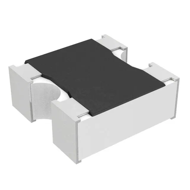
Chip Attenuator
Chip Attenuator
0404
Type:
EXB24AT (Unbalanced p type)
Type:
EXB24AB (Balanced O type)
n Features
EXB24AT type : Unbalanced p type
l Unbalanced p type attenuator circuit in one chip(1.0 mm ´ 1.0 mm)
l Mounting occupation area reduction : about 50 % reduction compared with an attenuator circuit consisting of
three 0402 chip resistors, almost equal to an attenuator circuit consisting of three 0201 chip resistors
l Mounting cost reduction : Mounting times 3 times Õ 1 time
l Attenuation : 1 dB to 10 dB
EXB24AB type : Balanced O type
l Balanced O type attenuator circuit in one chip(1.0 mm ´ 1.0 mm)
l Mounting occupation area reduction : about 64 % reduction compared with an attenuator circuit consisting of four
0402 chip resistors, about 26 % reduction compared with attenuator circuit consisting of four 0201 chip resistors
l Mounting cost reduction : Mounting times 4 times Õ 1 time
l Attenuation : 0 dB to 10 dB
n Recommended Applications
l Attenuation / level control / impedance matching of high frequency signals of communication equipment;
cellular phones(GSM, CDMA, PDC, etc.), PHS, PDA, for example.
�Chip Attenuator
n Explanation of Part Numbers
l EXB24AT type : Unbalanced p type
1
2
3
4
5
6
7
8
9
10
11
12
E
X
B
2
4
A
T
3
A
R
3
X
l EXB24AB type : Balanced O type
1
2
3
4
5
6
7
8
9
10
11
12
E
X
B
2
4
A
B
3
G
R
8
X
n Attenuation-Frequency Characteristics (typical) (EXB24AT type)
�Chip Attenuator
n Construction
EXB24AT
EXB24AB
EXB24AT
EXB24AB
n Circuit Configuration
n Dimensions (not to scale)
EXB24AT
Dimensions
(mm)
Dimensions
(mm)
EXB24AB
L
W
T
A
B
1.00±0.10
1.00+0.10
0.35±0.10
0.33±0.10
0.15±0.10
C
P(typical value)
0.25±0.10
0.65
The bar marking for recognizing terminal direction is
located on the side of terminal 4.
Dimensions
(mm)
Dimensions
(mm)
L
W
T
A
B
1.00±0.10
1.00+0.10
0.35±0.10
0.33±0.10
0.15±0.10
C
P(typical value)
0.30±0.10
0.65
�Chip Attenuator
n Ratings
Attenuation Value
EXB24AT
1 dB, 2 dB, 3 dB, 4 dB, 5 dB, 6 dB, 10 dB*
Attenuation Value Tolerance
1 dB, 2 dB, 3 dB, 4 dB, 5 dB : ± 0.3 dB
: ± 0.5 dB
6 dB, 10 dB
Item
Frequency Range
VSWR
0 dB to 3 dB : ± 0.8 dB
: ± 1.0 dB
10 dB
: ± 2.0 dB
100 W, 200 W, 300 W *
0.04 W /package
0.04 W /package
DC to 2 GHz
DC to 2.5 GHz
1.2 Max.(typical value)
1.3 Max.
(Voltage Standing Wave Ratio)
6 dB
50 W*
Characteristic Impedance
Power Rating
EXB24AB
0 dB, 1 dB, 2 dB, 3 dB, 6 dB, 10 dB*
1.5 Max.(0 dB, typical value)
Number of Resistors
3 resistors
4 resistors
Number of Terminals
4 terminals
4 terminals
-55 ¡C to +125 ¡C
-55 ¡C to +125 ¡C
Category Temperature Range
(Operating Temperature Range)
*Please inquire about the other attenuator value / characteristics impedance.
Power Derating Curve
For resistors operated in ambient temperature above
70¡C, power rating shall be derated in accordance
with the figure on the right.
n Packaging Methods
l Standard Quantity
Type
(inches)
EXB24AT/AB
(0404)
Thickness (mm)
Weight (mg)
Punched (Paper) Taping (2 mm Pitch)
0.35
1.1
10000 pcs./reel
n Taping Dimensions
l Taping Reel
Dimensions
fA
(mm)
180.0 Ð 03.0
l Punched (Paper) Taping
fB
60 min.
fC
13.0±1.0
W
9.0±1.0
T
Dimensions
11.4±2.0
(mm)
Dimensions
(mm)
A
B
W
F
1.20
1.20
8.00
3.50
P0
P1
P2
4.00
2.00
2.00
±0.05
±0.10
±0.05
±0.10
±0.20
±0.05
±0.05
fD 0
1.50
+0.10
0
E
1.75±0.10
T
0.45±0.10
Products shall be sealed so as to locate the terminal
1 and 2 on the side of feeding direction in the chip
pocket.
�Chip Attenuator
nRecommend Land Pattern
Dimensions
(mm)
a
0.5
b
0.35 to 0.4
c
0.3
d
1.4 to 1.5
Safety Precautions
1. Soldering
Recommendation for soldering method is noted below.
lReflow soldering
Precautions and recommendations are described below.
lPlease inquire with us when you use the different conditions.
lPlease measure a temperature of terminations and study the solderability for every type of board before using.
Rising temperature I
Preheating
Rising temperature II
Main heating
Gradual cooling
The normal to Preheating temperature
30 s to 60 s
140 ¡C to 160 ¡C
60 s to 120 s
Preheating to 200 ¡C
20 s to 40 s
(cf. The limits of resistance to reflow soldering heat)
200 ¡C to 100 ¡C
1 ¡C/s to 4 ¡C/s
(Reflow soldering shall be within two times.)
l Flow soldering
We cannot recommend the flow soldering, because a solder bridge may occur owing to
narrow 0.65 mm pitch.
l Iron soldering
1Solder at 280 ¡C max. and 3 seconds max. with the soldering iron tip.
2The soldering iron tip shall not touch the protective coating of the part.
l Use rosin type flux. Do not use high-activity flux (the chlorine content is 0.2 wt % or more).
l Allow enough preheating so that the difference of soldering temperature and temperature of surface of
the part is 100 ¡C or less. This temperature difference shall be kept in rapid cooling by immersion into
solvent.
l Use of more solder results in more mechanical stress to the part resulting in cracking or impaired
characteristics. Avoid excessive amount of solder.
2. Cleaning
l Residual flux after board washing may cause solder migration. Carefully check the status of board
washing.
Study the type and amount of flux to be used when no washing is made. Study the type of water-soluble flux
and cleaning agent and drying condition when water washing is done. Confirm they will not cause any
trouble.
3. Others
l Take necessary precautions to avoid any abnormal stress caused by bending of board.
l Do not use the product in dewy atmosphere.
�
很抱歉,暂时无法提供与“EXB-24AB6C1RX”相匹配的价格&库存,您可以联系我们找货
免费人工找货