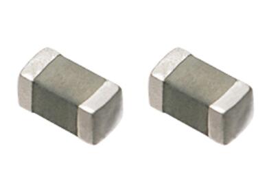
Multilayer Varistors
Multilayer Varistor for ESD pulse
[DC voltage lines/High speed signal lines]
Series: EZJZ, EZJP
Features
●
●
●
●
●
●
●
●
●
Excellent ESD suppression due to original advanced material technology
Having large electrostatic resistance meeting IEC61000-4-2, Level 4 standard
Having no polarity (bipolar) facilitated replacing Zener Diodes. Capable of replacing 2 Zener Diodes and 1 Capacitor.
Lead-free plating terminal electrodes enabling great solderability
Wide range of products is available by adopting multilayer structure, meeting various needs.
Low capacitance versions for DC voltage lines of high speed busses
Ultra low capacitance for high speed signal line
Applicable to high-speed signal lines, such as interfaces (e.g. USB 2.0, IEEE1394, HDMI, and so on), due to
our original ultra-low capacitance technology.
RoHS compliant
■ As for Packaging Methods, Handling Precautions
Please see Data Files
Explanation of Part Numbers
1
2
3
4
5
6
7
8
9
10
11
E
Z
J
Z
0
V
2
7
0
E
A
(Example)
Design Code
Product Code
Z
P
12
Series Code
EZJZ series
EZJP series
Packaging Style Code
V 0402, 0603 Paper Taping
Nominal Varitor Voltage
Size Code
Z
0
1
0201
0402
0603
The first and second digits
denote the first 2 numbers
of the varistor voltage and
the third digit indicates the
number of zeros following.
The decimal point denotes
in R.
A
R
D
E
W
F
Capacitance Code
3 pF
G 100 pF
20 pF
H 150 pF
27 pF
J 220 pF
47 pF
K 330 pF
56 pF M 680 pF
68 pF
Nil
B
C
D
K
M
Design Code
Cap. Tolerance : max.
Cap. Tolerance : ±0.1 pF
Cap. Tolerance : ±0.25 pF
Cap. Tolerance : ±0.50 pF
Cap. Tolerance : ±10 %
Cap. Tolerance : ±20 %
Below 3 pF, the 10 or 11th
position of the P/N indicates the
capacitance value as follows :
2.0 pF·····20, 1.5 p·····F15
Construction
3
4
5
Name
1
Semiconductive Ceramics
2
Internal electrode
3
2
1
No.
4
Substrate electrode
Terminal electrode
5
Intermediate electrode
External electrode
Dimensions in mm (not to scale)
L
W
Size Code Size(inch)
T
L1
L2
L
W
T
L1, L2
Z
0201
0.60±0.03
0.30±0.03
0.30±0.03
0.15±0.05
0
0402
1.00±0.05
0.50±0.05
0.50±0.05
0.2±0.1
1
0603
1.6±0.1
0.8±0.1
0.8±0.1
0.3±0.2
Design and specifications are each subject to change without notice. Ask factory for the current technical specifications before purchase and/or use.
Should a safety concern arise regarding this product, please be sure to contact us immediately.
04 Nov. 2016
�Multilayer Varistors
Multilayer Varistor, Low Capacitance Type
[High speed signal lines]
Features
●
●
●
●
Multilayer monolithic ceramic construction for high speed signal lines
Ideal for USB 2.0, IEEE1394, and HDMI high speed data busses
Applicable to high-speed signal lines, such as interfaces (e.g. USB 2.0, IEEE1394, HDMI, and so on), due to
our original material technology and multilayer technology.
Capacitance: 0.8 to 2.1 pF typ.
Recommended Applications
Mobile phone
DSC, DVC
PC, PDA
TV, DVD
Game console
Antenna circuit, External IF
USB2.0, IEEE1394
USB2.0, IEEE1394, LAN1000BASE
USB2.0, IEEE1394, HDMI
Controller, External IF
Ratings and Characteristics
Size
Part No.
EZJZ0V80010
Maximum
Nominal varistor
allowable voltage
voltage
DC (V)
at 1mA (V)
10
80
EZJZ0V80015D
0402
0603
● Operating
Capacitance (pF)
at 1MHz
Maximum ESD
IEC61000-4-2
1 max. [0.8 typ.]
5
80
1.5±0.5
EZJZ0V500AA
5
50
3 max. [2.1 typ.]
EZJZ0V800AA
18
80
3 max. [2.1 typ.]
EZJZ0V171AA
18
170
3 max. [2.1 typ.]
EZJZ1V80010
10
80
1 max. [0.8 typ.]
EZJZ1V500AA
5
50
3 max. [2.1 typ.]
EZJZ1V800AA
18
80
3 max. [2.1 typ.]
EZJZ1V171AA
18
170
3 max. [2.1 typ.]
Contact discharge : 8kV
Temperature Range: –40 to 85 °C
✽ Recommend soldering method : Reflow soldering
Voltage vs. Current
Max. Leakage Current
Max. Clamping Voltage
1000
1AA
Voltage (V)
EZJZ□V17
A
V800A
EZJZ□
EZJZ□V171AA
V500AA
EZJZ□
100
EZJZ□V800AA
A
EZJZ□V500A
(Typical curve)
10
10–6
10–5
10–4
10–3
10–2
10–1
100
101
Current (A)
Design and specifications are each subject to change without notice. Ask factory for the current technical specifications before purchase and/or use.
Should a safety concern arise regarding this product, please be sure to contact us immediately.
04 Nov. 2016
�Multilayer Varistors
Capacitance vs. Frequency
Impedance vs. Frequency
10000000
100
3 pF max. [2.1 pF typ.]
1000000
1 pF max. [0.8 pF typ.]
10
1
3 pF max. [2.1 pF typ.]
100000
Impedance (Ω)
Capacitance (pF)
1.5 pF typ.
1.5 pF typ.
1 pF max. [0.8 pF typ.]
10000
1000
100
10
(Typical curve)
(Typical curve)
0.1
1
10
100
Frequency (MHz)
1000
10000
1
1
10
100
Frequency (MHz)
1000
10000
Attenuation vs. Frequency
10
3 pFmax.[2.1pFtyp.]
1.5 pFtyp.
1 pFmax.[0.8pFtyp.]
5
Attenuation (dB)
0
–5
–10
–15
–20
–25
–30
–35
(Typical curve)
–40
1
10
100
Frequency (MHz)
1000
10000
Design and specifications are each subject to change without notice. Ask factory for the current technical specifications before purchase and/or use.
Should a safety concern arise regarding this product, please be sure to contact us immediately.
04 Nov. 2016
�Multilayer Varistors
Multilayer Varistor, Low Voltage Type (Standard Type)
[DC voltage lines/Low speed signal lines]
Features
Recommended Applications
Maximum allowable voltage
DC (V)
Wide variety of products is available by adopting
multilayer construction, which achieved wide
range of usage, such as application to DC
voltage lines and signal lines.
● Circuit voltage
40
30
26
16
13
11
6.7
5.6
3.7
Mobile phone
SW, LCD, LED, Audio terminal,
Battery pack, Memory card, External IF
DSC, DVC
SW, LCD, LED, USB
PC, PDA
SW, LCD, LED, USB
TV, DVD
Audio, Video terminal
Audio
Audio terminal, Microphone, Receiver
Game console
Controller, External IF
3 5
12 24 40
Circuit voltage DC (V)
● Varistor voltage : 6.8 to 65 V
● Capacitance : 8.5 to 420 pF
[at 1 mA]
typ. [at 1 MHz]
Ratings and Characteristics
Size
Part No.
EZJPZV6R8JA
EZJPZV6R8GA
EZJPZV080GA
EZJPZV120GA
0201 EZJPZV120DA
EZJPZV120RA
EZJPZV150RA
EZJPZV270RA
EZJPZV270BA
EZJP0V6R8MA
EZJP0V6R8GA
EZJP0V080MA
EZJP0V080KA
EZJP0V080GA
EZJP0V080DA
0402 EZJP0V120JA
EZJZ0V180HA
EZJZ0V220HA
EZJP0V270EA
EZJP0V270RA
EZJZ0V420WA
EZJZ0V650DA
EZJP1V120KA
EZJZ1V180JA
EZJZ1V220JA
EZJZ1V270GA
0603 EZJZ1V270EA
EZJZ1V270RA
EZJZ1V330GA
EZJZ1V420FA
EZJZ1V650DA
● Operating
Maximum Nominal
varistor
allowable
voltage
voltage
DC (V) at 1mA (V)
3.7
3.7
5.6
7.5
7.5
7.5
9
16
16
3.7
3.7
5.6
5.6
5.6
5.6
6.7
11
13
16
16
30
40
6.7
11
13
16
16
16
26
30
40
6.8
6.8
8
12
12
12
15
27
27
6.8
6.8
8
8
8
8
12
18
22
27
27
42
65
12
18
22
27
27
27
33
42
65
Capacitance (pF)
at 1MHz
220 max. [180 typ.]
100 max. [ 85 typ.]
100 max. [ 85 typ.]
100 max. [ 85 typ.]
27 max. [ 22 typ.]
20 max. [ 15 typ.]
20 max. [ 15 typ.]
20 max. [ 15 typ.]
10 max. [8.5 typ.]
680 max. [420 typ.]
100 max. [ 85 typ.]
680 max. [420 typ.]
330 max. [290 typ.]
100 max. [ 65 typ.]
27 max. [ 22 typ.]
220 max. [150 typ.]
150 max. [120 typ.]
150 max. [100 typ.]
47 max. [ 33 typ.]
20 max. [ 15 typ.]
56 max. [ 40 typ.]
27 max. [ 22 typ.]
330 max. [250 typ.]
220 max. [180 typ.]
220 max. [160 typ.]
100 max. [ 85 typ.]
47 max. [ 33 typ.]
20 max. [ 15 typ.]
100 max. [ 85 typ.]
68 max. [ 55 typ.]
27 max. [ 22 typ.]
Temperature Range: –40 to 85 °C
at 1kHz
175 typ.
100 typ.
100 typ.
100 typ.
33 typ.
18 typ.
18 typ.
16.5 typ.
10 typ.
650 typ.
100 typ.
650 typ.
480 typ.
100 typ.
33 typ.
175 typ.
140 typ.
116 typ.
37 typ.
16.5 typ.
45 typ.
33 typ.
290 typ.
210 typ.
185 typ.
100 typ.
37 typ.
16.5 typ.
100 typ.
63 typ.
33 typ.
Maximum
peak current
at 8/20µs, 2times
(A)
Maximum ESD
IEC61000-4-2
5
5
5
5
1
1
1
1
1
20
3
20
15
3
1
10
10
10
4
1
10
5
20
20
20
20
20
3
20
15
5
Contact discharge
8 kV
✽ Recommend soldering method : Reflow soldering
Maximum Allowable Voltage Maximum DC Voltage that can be applied continuously within the operating temperature range
Varistor Voltage
Varistor starting voltage between terminals at DC 1 mA, also known as Breakdown voltage
Maximum Peak Current
Maximum current that can be withstood under the standard pulse 8/20 µs, 2 times based
Maximum
voltage that can be withstood under ESD based on IEC61000-4-2, 10 times
Maximum ESD
(5 times of each positive-negative polarity)
Design and specifications are each subject to change without notice. Ask factory for the current technical specifications before purchase and/or use.
Should a safety concern arise regarding this product, please be sure to contact us immediately.
05
Feb. 2017
�Multilayer Varistors
Voltage vs. Current
EZJP Series
●
EZJZ Series
●
Max. Clamping Voltage
Max. Leakage Current
100
EZJP□V270RA
EZJPZV150RA
EZJPZV120GA
EZJP□V080□A
EZJP□V6R8□A
EZJP□V270RA
EZJZ□V650□A
EZJZ□V420□A
EZJZ□V330□A
EZJZ□V270□A
EZJZ□V220□A
EZJZ□V180□A
EZJZ□V120□A
Voltage (V)
Voltage (V)
EZJPZV150RA
Max. Clamping Voltage
Max. Leakage Current
300
200 EZJZ□V650□A
EZJZ□V420□A
100 EZJZ□V330□A
10
10
EZJZ□V270□A
EZJPZV120GA
EZJP□V080□A
EZJP□V6R8□A
EZJZ□V220□A
EZJZ□V180□A
EZJZ□V120□A
(Typical curve)
1
10–6
10–5
10–4
10–3
10–2
10–1
100
(Typical curve)
1
–6
10
10–5
10–4
101
10–3
Current (A)
10–2
10–1
Current (A)
100
101
102
Capacitance vs. Frequency
EZJP Series
10000
10000
680 pFmax.
330 pFmax.
1000
Capacitance (pF)
EZJZ Series
●
100 pFmax.
27 pFmax.
100
330 pF max.
220 pF max.
100 pF max.
1000
20 pFmax.
10 pFmax.
Capacitance (pF)
●
47 pF max.
100
20 pF max.
10
10
(Typical curve)
1
0.1
1
(Typical curve)
10
100
Frequency (MHz)
1000
1
0.1
10000
1
10
100
Frequency (MHz)
1000
10000
Attenuation vs. Frequency
●
EZJP Series
●
10 pFmax.
20 pFmax.
10
0
27 pFmax.
100 pFmax.
0
20 pF max.
47 pF max.
–10
Attenuation (dB)
–10
Attenuation (dB)
EZJZ Series
10
20
–30
330 pFmax.
680 pFmax.
–40
20
100 pF max.
–30
220 pF max.
330 pF max.
–40
–50
–50
(Typical curve)
–60
0.1
1
(Typical curve)
10
100
Frequency (MHz)
1000
10000
–60
0.1
1
10
100
Frequency (MHz)
1000
10000
Design and specifications are each subject to change without notice. Ask factory for the current technical specifications before purchase and/or use.
Should a safety concern arise regarding this product, please be sure to contact us immediately.
04 Nov. 2016
�Multilayer Varistors
Varistor Characteristics and Equivalent Circuit
A Multilayer Varistor does not have an electrical polarity like zener diodes and is equivalent to total 3 pcs.
of 2 zener diodes and 1 capacitor.
[Equivalent Circuit]
Current (A)
Zener diode
Zener diode
monopolar 2pcs.
Voltage (V)
Capacitor 1 pc.
Multilayer Varistor
ESD Suppressive Effects
Typical effects of ESD suppression
Test conditions: IEC61000-4-2✽ Level 4 Contact discharge, 8 kV
[ESD suppressed waveform]
1400
1200
Without Varistor
Electrostatic discharger
Voltage (V)
1000
Attenuator : 60 dB
330 Ω
50 Ω
Oscillo-scope
150 pF
800
EZJP0V080GA
[V1 mA:8 V, C1 MHz:100 pF max.]
600
400
200
0
MLCV
-200
–20
0
20
40
60
80
100 120
Time (ns)
140
160
180
200
✽ IEC61000-4-2 ··· International Standard of the ESD testing method (HBM) for electronic equipment ability to
withstand ESD generated from a human body. It sets 4 levels of severity
Severity
Contact discharge
Air discharge
Level 1
2 kV
2 kV
Level 2
4 kV
4 kV
Level 3
6 kV
8 kV
Level 4
8 kV
15 kV
Replacement of Zener diode
Replacing “Zener diode and Capacitor” with Multilayer Varistor saves both the mounting area and number
of components used.
1.7
0.3
0.5
2.6
Zener diode
S-79
Mounting area
Approx .83 % space saving
MLCC
Size 0402
1.5
MLCV
Size 0402
Dimensions in mm
Design and specifications are each subject to change without notice. Ask factory for the current technical specifications before purchase and/or use.
Should a safety concern arise regarding this product, please be sure to contact us immediately.
04 Nov. 2016
�Multilayer Varistors
Recommended Applications
Applications
Series
Mobile phones, DSC, PC, PDA,
Series
HDD TV (PDP, LC etc.), DVD, DVC,
EZJZ, P
Game consoles, Audio equipment
PWR, Photoelectronic sensors,
SSR, Motors, Pressure sensors,
Proximity switches
DC 1k
1M
Circuit
1G (Hz)
DC to GHz
Antenna, RF circuit, LVDS
USB, IEEE1394, HDMI etc.
DC to tens of Hz
PWR, SW, Audio terminals
LCD, RS232C, etc.
Ultra low capacitance
(Cap. : 3 pF or less)
Low capacitance
(Cap. : 20 to 680 pF)
Series
High capacitance
EZJS (Cap. : 1800 to 22000 pF)
DC to several kHz
PWR, SW, Audio terminals etc.
Applications
●
Mobile Phone
· Audio lines
· LCD/Camera lines
2 mode noise filter
AMP
LCD/Camera
controller
FPC
LCD/Camera
· LED
IC
· I/O data lines
· SW/Keyboard
I/O
controller
Connector
IC
●
USB1.1/2.0 lines
●
IEEE1394 lines
VDD
Power
IC
D+
USB
controller
D–
GND
IEEE1394
controller
VDD
GND
TPA+
TPA–
TPB+
TPB–
●
HDMI lines
HDMI
IC
Ch : 0
Ch : 1
Ch : 2
TMDS
Connector
Clock
Design and specifications are each subject to change without notice. Ask factory for the current technical specifications before purchase and/or use.
Should a safety concern arise regarding this product, please be sure to contact us immediately.
04 Nov. 2016
�Multilayer Varistors
Performance and Testing Methods
Characteristics
Specifications
Standard test
conditions
Testing Method
Electrical characteristics shall be measured under the following conditions.
Temp. : 5 to 35 °C, Relative humidity : 85 % or less
Varistor voltage
The Varistor voltage is the voltage (VC,or VcmA) between both end terminals of a
To meet the specified
Varistor when specified current (CmA) is applied to it. The measurement shall be
value.
made as quickly as possible to avoid heating effects.
Maximum
allowable voltage
To meet the specified
The maximum DC voltage that can be applied continuously to a varistor.
value.
Capacitance
To meet the specified Capacitance shall be measured at the specified frequency, bias voltage 0 V,
value.
and measuring voltage 0.2 to 2 Vrms.
Maximum peak
current
The maximum current measured (Varistor voltage tolerance is within ±10 %)
To meet the specified
when a standard impulse current of
value.
8/20 µ seconds is applied twice with an interval of 5 minutes.
Maximum ESD
The maximum ESD measured (while the varistor voltage is within ±30 % of its
To meet the specified
nominal value) when exposed to ESD 10 times
value.
(five times for each positive-negative polarity) based on IEC61000-4-2.
Solder ability
The part shall be immersed into a soldering bath under the conditions below.
Solder: H63A
Soldering flux
: Ethanol solution of rosin (Concentration approx. 25 wt%)
To meet the specified
Soldering temp. : 230±5 °C
value.
Period
: 4±1 s
Soldering position : Immerse both terminal electrodes until they are completely
into the soldering bath.
Resistance to
soldering heat
After the immersion, leave the part for 24 ±2 hours under the standard condition,
then evaluate its characteristics.Soldering conditions are specified below:
ΔVc / Vc : within ±10 % Soldering conditions : 270 °C, 3 s / 260 °C, 10 s
Soldering position : Immerse both terminal electrodes until they are completely
into the soldering bath.
After repeating the cycles stated below for specified number of times, leave
the part for 24±2 hours, then evaluate its characteristics.
Cycle : 5 cycles
Temperature
cycling
ΔVc / Vc : within ±10 %
Step
Temperature
Period
1
Max. Operating Temp.
30±3 min
2
Ordinary temp.
3 min max.
3
Min. Operating Temp.
30±3 min
4
Ordinary temp.
3 min max.
Biased Humidity
After conducting the test under the conditions specified below, leave the part
24±2 hours, then evaluate its characteristics.
Temp.
: 40±2 °C
ΔVc / Vc : within ±10 %
Humidity
: 90 to 95 %RH
Applied voltage : Maximum allowable voltage (Individually specified)
Period
: 500+24 / 0 h
High temperature
exposure
(dry heat)
After conducting the test under the conditions specified below, leave the part
24 ±2 hours, then evaluate its characteristics.
ΔVc / Vc : within ±10 % Temp.
: Maximum operating temperature ±3 °C (Individually specified)
Applied voltage : Maximum allowable voltage (Individually specified)
Period
: 500+24 / 0h
Design and specifications are each subject to change without notice. Ask factory for the current technical specifications before purchase and/or use.
Should a safety concern arise regarding this product, please be sure to contact us immediately.
04 Nov. 2016
�*XLGHOLQHV�DQG�SUHFDXWLRQV�UHJDUGLQJ�WKH
WHFKQLFDO�LQIRUPDWLRQ�DQG�XVH�RI�RXU�SURGXFWV
GHVFULEHG�LQ�WKLV�RQOLQH�FDWDORJ�
�ٹ,I�\RX�ZDQW�WR�XVH�RXU�SURGXFWV�GHVFULEHG�LQ�WKLV�RQOLQH�FDWDORJ�IRU�DSSOLFDWLRQV�UHTXLULQJ�
�VSHFLDO�TXDOLWLHV�RU�UHOLDELOLW\��RU�IRU�DSSOLFDWLRQV�ZKHUH�WKH�IDLOXUH�RU�PDOIXQFWLRQ�RI�WKH�
�SURGXFWV�PD\�GLUHFWO\�MHRSDUGL]H�KXPDQ�OLIH�RU�SRWHQWLDOO\�FDXVH�SHUVRQDO�LQMXU\�
��H�J��DLUFUDIW�DQG�DHURVSDFH�HTXLSPHQW��WUDIILF�DQG�WUDQVSRUWDWLRQ�HTXLSPHQW��FRPEXVWLRQ�
�HTXLSPHQW��PHGLFDO�HTXLSPHQW��DFFLGHQW�SUHYHQWLRQ��DQWL�FULPH�HTXLSPHQW��DQG�RU�VDIHW\�
�HTXLSPHQW���LW�LV�QHFHVVDU\�WR�YHULI\�ZKHWKHU�WKH�VSHFLILFDWLRQV�RI�RXU�SURGXFWV�ILW�WR�VXFK�
�DSSOLFDWLRQV��3OHDVH�HQVXUH�WKDW�\RX�ZLOO�DVN�DQG�FKHFN�ZLWK�RXU�LQTXLU\�GHVN�DV�WR�ZKHWKHU
�WKH�VSHFLILFDWLRQV�RI�RXU�SURGXFWV�ILW�WR�VXFK�DSSOLFDWLRQV�XVH�EHIRUH�\RX�XVH�RXU�SURGXFWV�
�ٹ7KH�TXDOLW\�DQG�SHUIRUPDQFH�RI�RXU�SURGXFWV�DV�GHVFULEHG�LQ�WKLV�RQOLQH�FDWDORJ�RQO\�DSSO\�
�WR�RXU�SURGXFWV�ZKHQ�XVHG�LQ�LVRODWLRQ��7KHUHIRUH��SOHDVH�HQVXUH�\RX�HYDOXDWH�DQG�YHULI\�
�RXU�SURGXFWV�XQGHU�WKH�VSHFLILF�FLUFXPVWDQFHV�LQ�ZKLFK�RXU�SURGXFWV�DUH�DVVHPEOHG�LQ�\RXU�
�RZQ�SURGXFWV�DQG�LQ�ZKLFK�RXU�SURGXFWV�ZLOO�DFWXDOO\�EH�XVHG�
�ٹ,I�\RX�XVH�RXU�SURGXFWV�LQ�HTXLSPHQW�WKDW�UHTXLUHV�D�KLJK�GHJUHH�RI�UHOLDELOLW\��UHJDUGOHVV�
�RI�WKH�DSSOLFDWLRQ��LW�LV�UHFRPPHQGHG�WKDW�\RX�VHW�XS�SURWHFWLRQ�FLUFXLWV�DQG�UHGXQGDQF\�
�FLUFXLWV�LQ�RUGHU�WR�HQVXUH�VDIHW\�RI�\RXU�HTXLSPHQW�
�ٹ7KH�SURGXFWV�DQG�SURGXFW�VSHFLILFDWLRQV�GHVFULEHG�LQ�WKLV�RQOLQH�FDWDORJ�DUH�VXEMHFW�WR�
�FKDQJH�IRU�LPSURYHPHQW�ZLWKRXW�SULRU�QRWLFH��7KHUHIRUH��SOHDVH�EH�VXUH�WR�UHTXHVW�DQG�
�FRQILUP�WKH�ODWHVW�SURGXFW�VSHFLILFDWLRQV�ZKLFK�H[SODLQ�WKH�VSHFLILFDWLRQV�RI�RXU�SURGXFWV�LQ�
�GHWDLO��EHIRUH�\RX�ILQDOL]H�WKH�GHVLJQ�RI�\RXU�DSSOLFDWLRQV��SXUFKDVH��RU�XVH�RXU�SURGXFWV�
�ٹ7KH�WHFKQLFDO�LQIRUPDWLRQ�LQ�WKLV�RQOLQH�FDWDORJ�SURYLGHV�H[DPSOHV�RI�RXU�SURGXFWV
�
�W\SLFDO�RSHUDWLRQV�DQG�DSSOLFDWLRQ�FLUFXLWV��:H�GR�QRW�JXDUDQWHH�WKH�QRQ�LQIULQJHPHQW�RI�
�WKLUG�SDUW\
V�LQWHOOHFWXDO�SURSHUW\�ULJKWV�DQG�ZH�GR�QRW�JUDQW�DQ\�OLFHQVH��ULJKW��RU�LQWHUHVW�
LQ�RXU�LQWHOOHFWXDO�SURSHUW\�
�ٹ,I�DQ\�RI�RXU�SURGXFWV��SURGXFW�VSHFLILFDWLRQV�DQG�RU�WHFKQLFDO�LQIRUPDWLRQ�LQ�WKLV�RQOLQH�
�FDWDORJ�LV�WR�EH�H[SRUWHG�RU�SURYLGHG�WR�QRQ�UHVLGHQWV��WKH�ODZV�DQG�UHJXODWLRQV�RI�WKH�
�H[SRUWLQJ�FRXQWU\��HVSHFLDOO\�ZLWK�UHJDUG�WR�VHFXULW\�DQG�H[SRUW�FRQWURO��VKDOO�EH�REVHUYHG��
�5HJDUGLQJ�WKH�&HUWLILFDWH�RI�&RPSOLDQFH�ZLWK�
WKH�(8�5R+6�'LUHFWLYH�5($&+�5HJXODWLRQV!
�ٹ7KH�VZLWFKRYHU�GDWH�IRU�FRPSOLDQFH�ZLWK�WKH�5R+6�'LUHFWLYH�5($&+�5HJXODWLRQV�YDULHV�
�GHSHQGLQJ�RQ�WKH�SDUW�QXPEHU�RU�VHULHV�RI�RXU�SURGXFWV�
�ٹ:KHQ�\RX�XVH�WKH�LQYHQWRU\�RI�RXU�SURGXFWV�IRU�ZKLFK�LW�LV�XQFOHDU�ZKHWKHU�WKRVH�SURGXFWV�
�DUH�FRPSOLDQW�ZLWK�WKH�5R+6�'LUHFWLYH�5($&+�5HJXODWLRQ��SOHDVH�VHOHFW��6DOHV�,QTXLU\��LQ�WKH�
�ZHEVLWH�LQTXLU\�IRUP�DQG�FRQWDFW�XV�
:H�GR�QRW�WDNH�DQ\�UHVSRQVLELOLW\�IRU�WKH�XVH�RI�RXU�SURGXFWV�RXWVLGH�WKH�VFRSH�RI�WKH�
VSHFLILFDWLRQV��GHVFULSWLRQV��JXLGHOLQHV�DQG�SUHFDXWLRQV�GHVFULEHG�LQ�WKLV�RQOLQH�FDWDORJ�
���$SU���
�Multilayer Varistors
Multilayer Varistors,Chip Type
Series: EZJZ, EZJP (For DC voltage lines, high speed signal lines)
Series: EZJS (For DC voltage lines)
Handling Precautions
[Precautions]
・ Do not use the products beyond the descriptions in this product catalog.
・ This product catalog guarantees the quality of the products as individual components.
Before you use the products, please make sure to check and evaluate the products
in the circumstance where they are installed in your product.
Safety Precautions
Multilayer Varistors (hereafter referred to as “Varistors”) should be used for general purpose applications as
countermeasures against ESD and noise found in consumer electronics (audio/visual, home, office, information
& communication) equipment. When subjected to severe electrical, environmental, and/or mechanical stress
beyond the specifications, as noted in the Ratings and Specified Conditions section, the Varistors’ performance
may be degraded, or become failure mode, such as short circuit mode and open-circuit mode.
If you use under the condition of short-circuit, heat generation of Varistors will occur by running large current
due to application of voltage. There are possibilities of smoke emission, substrate burn-out, and, in the worst
case, fire. For products which require high safety levels, please carefully consider how a single malfunction can
affect your product. In order to ensure the safety in the case of a single malfunction, please design products
with fail-safe, such as setting up protecting circuits, etc.
We are trying to improve the quality and the reliability, but the durability differs depending on the use
environment and the use conditions. On use, be sure to confirm the actual product under the actual use
conditions.
● For the following applications and conditions, please be sure to consult with our sales representative in
advance and to exchange product specifications which conform to such applications.
・ When your application may have difficulty complying with the safety or handling precautions specified below.
・ High-quality and high-reliability required devices that have possibility of causing hazardous conditions, such
as death or injury (regardless of directly or indirectly), due to failure or malfunction of the product.
① Aircraft and Aerospace Equipment (artificial satellite, rocket, etc.)
② Submarine Equipment (submarine repeating equipment, etc.)
③ Transportation Equipment (motor vehicles, airplanes, trains, ship, traffic signal controllers, etc.)
④ Power Generation Control Equipment
(atomic power, hydroelectric power, thermal power plant control system, etc.)
⑤ Medical Equipment (life-support equipment, pacemakers, dialysis controllers, etc.)
⑥ Information Processing Equipment (large scale computer systems, etc.)
⑦ Electric Heating Appliances, Combustion devices (gas fan heaters, oil fan heaters, etc.)
⑧ Rotary Motion Equipment
⑨ Security Systems
⑩ And any similar types of equipment
Strict Observance
1. Confirmation of Rated Performance
The Varistors shall be operated within the specified rating/performance.
Applications exceeding the specifications may cause deteriorated performance and/or breakdown, resulting in
degradation and/or smoking or ignition of products. The following are strictly observed.
(1) The Varistors shall not be operated beyond the specified operating temperature range.
(2) The Varistors shall not be operated in excess of the specified maximum allowable voltage.
(3) The Varistors shall not be operated in the circuits to which surge current and ESD that exceeds the specified
maximum peak current and maximum ESD.
(4) Never use for AC power supply circuits.
2. The Varistors shall not be mounted near flammables.
01. Oct. 2019
�Multilayer Varistors
Operating Conditions and Circuit Design
1. Circuit Design
1.1 Operating Temperature and Storage Temperature
When operating a components-mounted circuit, please be sure to observe the “Operating Temperature Range”,
written in delivery specifications. Storage temperature of PCB after mounting Varistors, which is not operated,
should be within the specified “Storage Temperature Range” in the delivery specifications. Please remember not
to use the product under the condition that exceeds the specified maximum temperature.
1.2 Operating Voltage
The Varistors shall not be operated in excess of the “Maximum allowable voltage”. If the Varistors are operated
beyond the specified Maximum allowable voltage, it may cause short and/or damage due to thermal run away.
The circuit that continuously applies high frequency and/or steep pulse voltage please examines the reliability of
the Varistor even if it is used within a “Maximum allowable voltage”. Also, it would be safer to check also the
safety and reliability of your circuit.
1.3 Self-heating
The surface temperature of the Varistors shall be under the specified Maximum Operating Temperature in the
Specifications including the temperature rise caused by self-heating. Check the temperature rise of the Varistor
in your circuit.
1.4 Environmental Restrictions
The Varistors does not take the use under the following special environments into consideration.
Accordingly, the use in the following special environments, and such environmental conditions may affect the
performance of the product; prior to use, verify the performance, reliability, etc. thoroughly.
① Use in liquids such as water, oil, chemical, and organic solvent.
② Use under direct sunlight, in outdoor or in dusty atmospheres.
③ Use in places full of corrosive gases such as sea breeze, Cl2,H2S,NH3,SO2,and NOx.
④ Use in environment with large static electricity or strong electromagnetic waves or strong radial ray.
⑤ Where the product is close to a heating component, or where an inflammable such as a polyvinyl chloride
wire is arranged close to the product.
⑥ Where this product is sealed or coated with resin etc.
⑦ Where solvent, water, or water-soluble detergent is used in flux cleaning after soldering.
(Pay particular attention to water-soluble flux.)
⑧ Use in such a place where the product is wetted due to dew condensation.
⑨ Use the product in a contaminated state.
Ex.) Do not handle the product such as sticking sebum directly by touching the product after mounting
printed circuit board.
⑩ Under severe conditions of vibration or impact beyond the specified conditions found in the Specifications.
2. Design of Printed Circuit Board
2.1 Selection of Printed Circuit Boards
There is a possibility of performance deterioration by heat shock (temperature cycles), which causes cracks,
from alumina substrate. Please confirm that the substrate you use does not deteriorate the Varistors’ quality.
2.2 Design of Land Pattern
1) Recommended land dimensions are shown below. Use the proper amount of solder in order to prevent cracking.
Using too much solder places excessive stress on the Varistors.
Recommended Land Dimensions(Ex.)
Unit (mm)
SMD
Component dimensions
Size
Code/EIA L
W
T
c
Land
b
a
Solder resist
Z(0201)
0.6
0.3
0.3
0(0402)
1.0
0.5
0.5
1(0603)
1.6
0.8
0.8
2(0805)
2.0
a
b
0.2 to 0.3 0.25 to 0.30
0.4 to 0.5
0.8 to 1.0
1.25 0.8 to 1.25 0.8 to 1.2
0.4 to 0.5
0.6 to 0.8
0.8 to 1.0
c
0.2 to 0.3
0.4 to 0.5
0.6 to 0.8
0.8 to 1.0
01. Oct. 2019
�Multilayer Varistors
c
b
SMD
Size
Code/EIA
S
Land
(0504 2Array)
Unit (mm)
Component dimensions
L
W
T
1.37
1.0
0.6
a
b
c
P
0.3 to 0.45 to 0.3 to 0.54 to
0.4
0.55
0.4
0.74
P
(2) The land size shall be designed to have equal space, on both right and left side. If the amount of solder on
the right land is different from that of the left land, the component may be cracked by stress since the side
with a larger amount of solder solidifies later during cooling.
Recommended Amount of Solder
(a) Excessive amount
2.3 Utilization of Solder Resist
(1) Solder resist shall be utilized to equalize
the amounts of solder on both sides.
(2) Solder resist shall be used to divide the
pattern for the following cases;
・ Components are arranged closely.
・ The Varistor is mounted near
a component with lead wires.
・ The Varistor is placed near a chassis.
See the table right.
(b) Proper amount
(c) Insufficient amount
Prohibited Applications and Recommended Applications
Mixed
mounting
with a
component
with lead
wires
The lead wire of a Component
With lead wires
Arrangement
near
chassis
Solder(ground solder)
Solder resist
Solder resist
Electrode pattern
A lead wire of Retrofitted
component
Lateral
arrangement
Solder resist
Solderingiron
iron
Portion to be
(1)To minimize mechanical stress caused
by the warp or bending of a PC board,
please follow the recommended Varistors’
layout below.
by pattern division
Chassis
Retro-fitting
of component
with lead
wires
2.4 Component Layout
To prevent the crack of Varistors, place it
on the position that could not easily be
affected by the bending stress of substrate
while going through procedures after
mounting or handling.
Improved applications
Prohibited
applications
Item
Excessively soldered
Solder resist
Land
Prohibited layout
Recommended layout
Layout the Varistors sideways
against the stressing direction.
01. Oct. 2019
�Multilayer Varistors
(2) The following layout is for your reference since
mechanical stress near the dividing/breaking
position of a PC board varies depending on
the mounting position of the Varistors.
E
Perforation
D
C
Magnitude of stress
A>B=C>D>E
A
Slit
B
(3) The magnitude of mechanical stress applied to the Varistors when dividing the circuit board in descending
order is as follows: push back < slit < V-groove < perforation. Also take into account the layout of the
Varistors and the dividing/breaking method.
2.5 Mounting Density and Spaces
Intervals between components should not be too narrow to prevent the influence from solder bridges
and solder balls. The space between components should be carefully determined.
Precautions for Assembly
1. Storage
(1) The Varistors shall be stored between 5 to 40 °C and 20 to 70 % RH, not under severe conditions of high
temperature and humidity.
(2) If stored in a place where humidity, dust, or corrosive gasses (hydrogen sulfide, sulfurous acid, hydrogen
chloride and ammonia, etc.) are contained, the solderability of terminals electrodes will be deteriorated.
In addition, storage in a place where the heat or direct sunlight exposure occurs will causes or direct sunlight
exposure occurs will causes mounting problems due to deformation of tapes and reels and components and
taping/reels sticking together.
(3) Do not store components longer than 6 months. Check the solderability of products that have been stored
for more than 6 months before use.
2. Adhesives for Mounting
(1) The amount and viscosity of an adhesive for mounting shall be such that the adhesive will not flow off on
the land during its curing.
(2) If the amount of adhesive is insufficient for mounting, the Varistors may fall off after or during soldering.
(3) Low-viscosity of the adhesive causes displacement of Varistors.
(4) The heat-curing methods for adhesive are ultraviolet radiation, far-infrared radiation, and so on.
In order to prevent the terminal electrodes of the Varistors from oxidizing, the curing shall be under the
following conditions:160 °C max., for 2 minutes max.
(5) Insufficient curing may cause the Varistors to fall off after or during soldering. In addition, insulation
resistance between terminal electrodes may deteriorate due to moisture absorption. In order to prevent
these problems, please observe proper curing conditions.
3. Chip Mounting Consideration
(1) When mounting the Varistors components on a PC board, the Varistor bodies shall be free from excessive
impact loads such as mechanical impact or stress due to the positioning, pushing force and displacement
of vacuum nozzles during mounting.
(2) Maintenance and inspection of the Chip Mounter must be performed regularly.
(3) If the bottom dead center of the vacuum nozzle is too low, the Varistor will crack from excessive force
during mounting. Pease refer to the following precautions and recommendations.
(a) Set and adjust the bottom dead center of the vacuum nozzles to the upper surface of the PC board
after correcting the warp of the PC board.
(b) Set the pushing force of the vacuum nozzle during mounting to 1 to 3 N in static load.
(c) For double surface mounting, apply a supporting pin on the rear surface of the PC board to suppress the
bending of the PC board in order to minimize the impact of the vacuum nozzles. Typical examples are
shown in the table belowsecondary.
(d) Adjust the vacuum nozzles so that their bottom dead center during mounting is not too low.
01. Oct. 2019
�Multilayer Varistors
Item
Prohibited mounting
Single
surface
mounting
Double
surface
mounting
Recommended mounting
The supporting pin
Crack
does not necessarily
have to be positioned
Separation of
Crack
Supporting
pin
Supporting
pin
(4) The closing dimensions of the positioning chucks shall be controlled. Maintenance and replacement of
positioning chucks shall be performed regularly to prevent chipping or cracking of the Varistors caused
by mechanical impact during positioning due to worn positioning chucks.
(5) Maximum stroke of the nozzle shall be adjusted so that the maximum bending of PC board does not
exceed 0.5 mm at 90 mm span. The PC board shall be supported by an adequate number of supporting pins.
4. Selection of Soldering Flux
Soldering flux may seriously affect the performance of the Varistors. Please confirm enough whether the
soldering flux have an influence on performance of the Varistors or not, before using.
5. Soldering
5.1 Flow Soldering
When conducting flow soldering, stress from abrupt temperature change is applied to the Varistors, so the
temperature, especially temperature of solder should be controlled very carefully. Varistors should not be
subjected to abrupt temperature change because it causes occurrence of thermal cracks as a result of
excessive thermal stress inside of the Varistors from flow soldering. You should be careful to temperature
difference. Therefore it is essential that solderinprocess follow these recommended conditions.
(1) Application of Soldering flux :
The soldering flux shall be applied to the mounted Varistors thinly and uniformly by foaming method.
(2) Preheating : Conduct sufficient pre-heating, and make sure that the temperature difference between
solder and Varistors’ surface is 150 °C or less.
(3) Immersion into Soldering bath :
The Varistors shall be immersed into a soldering bath of 240 to 260 °C for 3 to 5 seconds.
(4) Gradual Cooling : After soldering, avoid rapid cooling (forced cooling) and conduct gradual cooling,
so that thermal cracks do not occur.
(5) Flux Cleaning : When the Varistors are immersed into a cleaning solvent, be sure that the surface
temperatures of devices do not exceed 100 °C.
(6) Performing flow soldering once under the conditions shown in the figure below
[Recommended profile of Flow soldering (Ex.)] will not cause any problems.
However, pay attention to the possible warp and bending of the PC board.
Soldering
260
240
Gradual cooling
(at ordinary
mperature)
△T
Temperature (˚C)
Recommended profile of Flow Soldering (Ex.)
0
Time
60 ot 120 s
Size/EIA
0603
Temp. Tol.
T ≦150 °C
3 to 5 s
For products specified in individual specifications, avoid flow soldering.
01. Oct. 2019
�Multilayer Varistors
5.2 Reflow Soldering
The reflow soldering temperature conditions are composed of temperature curves of Preheating, Temp. rise,
Heating, Peak and Gradual cooling. Large temperature difference inside the Varistors caused by rapid heat
application to the Varistors may lead to excessive thermal stresses, contributing to the thermal cracks. The
Preheating temperature requires controlling with great care so that tombstone phenomenon may be prevented.
260
220
②Temp.
③Gradual
cooling
180
140
①Preheating
③Heating
60 ot 120 s
Item
① Preheating
④Peak
△T
Temperature (˚C)
Recommended profile of Reflow Soldering (Ex.)
60 s max.
Time
② Temp. rise
③ Heating
④ Peak
⑤ Gradual
cooling
Temperature
140 to 180 ℃
Preheating temp
to Peak temp.
220 ℃ min.
260 ℃ max.
Peak temp.
to 140 ℃
Size/EIA
0201 to 0805, 0504
Period or Speed
60 to 120 s
2 to 5 ℃ / s
60 s max.
10 s max.
1 to 4 ℃ / s
Temp. Tol.
T ≦150 °C
△T : Allowable temperature difference △T≦ 150 °C
The rapid cooling (forced cooling) during Gradual cooling part should be avoided, because this may cause defects
such as the thermal cracks, etc. When the Varistors are immersed into a cleaning solvent, make sure that the
surface temperatures of the devices do not exceed 100 °C. Performing reflow soldering twice under the conditions
shown in the figure above [Recommended profile of Flow soldering (Ex.)] will not cause any problems.
However, pay attention to the possible warp and bending of the PC board.
Recommended soldering condition is for the guideline for ensuring the basic characteristics of the components,
not for the stable soldering conditions. Conditions for proper soldering should be set up according to individual
conditions. The temperature of this product at the time of mounting changes depending on mounting conditions,
therefore, please confirm that Product surface becomes the specified temperature when mounting it on the end
product.
5.3 Hand Soldering
Hand soldering typically causes significant temperature change, which may induce excessive thermal stresses
inside the Varistors, resulting in the thermal cracks, etc. In order to prevent any defects, the following should be
observed.
· Control the temperature of the soldering tips with special care.
· Avoid the direct contact of soldering tips with the Varistors and/or terminal electrodes.
· Do not reuse dismounted Varistors.
(1) Condition 1 (with preheating)
(a) Soldering : Use thread solder (φ 1.0 mm or below) which contains flux with low chlorine, developed for
precision electronic equipment.
(b) Preheating : Conduct sufficient preheating, and make sure that the temperature difference between solder
and Varistors’ surface is 150 °C or less.
(c) Temperature of Iron tip: 300 °C max.
(The required amount of solder shall be melted in advance on the soldering tip.)
(d) Gradual cooling : After soldering, the Varistors shall be cooled gradually at room temperature.
Recommended profile of Hand soldering (Ex.)
△T
Gradual
cooling
Preheating
60 ot 120 s
3 s max.
△T : Allowable temperature difference △T ≦ 150 °C
01. Oct. 2019
�Multilayer Varistors
(2) Condition 2 (without preheating)
Hand soldering can be performed without preheating,
Conditions of Hand soldering without preheating
by following the conditions below:
(a) Soldering iron tip shall never directly touch the
ceramic and terminal electrodes of the Varistors.
(b) The lands are sufficiently preheated with a soldering
iron tip before sliding the soldering iron tip to the
terminal electrodes of the Varistors for soldering.
Item
Condition
Temperature of Iron tip
Wattage
Shape of Iron tip
Soldering time with a
soldering iron
270 ℃ max.
20 W max.
φ 3 mm max.
3 s max.
6. Post Soldering Cleaning
6.1 Cleaning solvent
Soldering flux residue may remain on the PC board if cleaned with an inappropriate solvent.
This may deteriorate the performance of Varistors, especially insulation resistance.
6.2 Cleaning conditions
Inappropriate cleaning conditions such as insufficient cleaning or excessive cleaning may impair the electrical
characteristics and reliability of the Varistors.
(1) Insufficient cleaning can lead to :
(a) The halogen substance found in the residue of the soldering flux may cause the metal of terminal electrodes
to corrode.
(b) The halogen substance found in the residue of the soldering flux on the surface of the Varistors may change
resistance values.
(c) Water-soluble soldering flux may have more remarkable tendencies of (a) and (b) above compared to those
of rosin soldering flux.
(2) Excessive cleaning can lead to :
(a) When using ultrasonic cleaner, make sure that the output is not too large, so that the substrate will not
resonate. The resonation causes the cracks in Varistors and/or solders, and deteriorates the strength of the
terminal electrodes. Please follow these conditions for Ultrasonic cleaning:
Ultrasonic wave output : 20 W/L max.
Ultrasonic wave frequency : 40 kHz max.
Ultrasonic wave cleaning time : 5 min. max.
6.3 Contamination of Cleaning solvent
Cleaning with contaminated cleaning solvent may cause the same results as that of insufficient cleaning
due to the high density of liberated halogen.
7. Inspection Process
The pressure from measuring terminal pins might bend the PCB when implementing circuit inspection
after mounting Varistors on PCB, and as a result, cracking may occur.
(1) Mounted PC boards shall be supported by an adequate number of supporting pins on the back with bend
settings of 90 mm span 0.5 mm max.
(2) Confirm that the measuring pins have the right tip shape, are equal in height, have the right pressure and
are set in the correct positions. The following figures are for your reference to avoid bending the PC board.
Item
Prohibited mounting
Check pin
Bending of
PC board
Separated, Crack
Recommended mounting
Check pin
Supporting pin
8.Protective Coating
Make sure characteristics and reliability when using the resin coating or resin embedding for the purpose of
improvement of humidity resistance or gas resistance, or fixing of parts because failures of a thermistors such
as 1) ,2) and 3) may be occurred.
(1) The solvent which contained in the resin permeate into the Varistors, and it may deteriorate the
characteristic.
01. Oct. 2019
�Multilayer Varistors
(2) When hardening the resin, chemical reaction heat (curing heat generation) happen and it may occurs the
infection to the Varistors.
(3) The lead wire might be cut down and the soldering crack might be happen by expansion or contraction of resin
hardening.
9. Dividing/Breaking of PC Boards
(1) Please be careful not to stress the substrate with bending/twisting when dividing, after mounting
components including Varistors. Abnormal and excessive mechanical stress such as bending or
torsion shown below can cause cracking in the Varistors.
Torsion
Bending
(2) Dividing/Breaking of the PC boards shall be done carefully at moderate speed by using a jig or apparatus to
prevent the Varistors on the boards from mechanical damage.
(3) Examples of PCB dividing/breaking jigs: The outline of PC board breaking jig is shown below. When PC board
are broken or divided, loading points should be close to the jig to minimize the extent of the bending.
Also, planes with no parts mounted on should be used as plane of loading, in order to prevent tensile stress
induced by the bending, which may cause cracks of the Varistors or other parts mounted on the PC boards.
Outline of Jig
Prohibited mounting
Recommended mounting
V-groove
PC board
Loading
point
PC
board
PC board
Loading direction
component
V-groove
PC
board
V-groove
Loading direction
component
Loading point
splitting jig
10. Mechanical Impact
(1) The Varistors shall be free from any excessive mechanical impact. The Varistor body is made of ceramics
and may be damaged or cracked if dropped. Never use a Varistor which has been dropped; their quality may
already be impaired, and in that case, failure rate will increase.
(2) When handling PC boards with Varistors mounted on them, do not allow the Varistors to collide with another PC
board. When mounted PC boards are handled or stored in a stacked state, the corner of a PC board might strike
Varistors, and the impact of the strike may cause damage or cracking and can deteriorate the withstand voltage
and insulation resistance of the Varistor.
Crack
Mounted
PCB
Crack
Floor
11. Do not reuse this product after removal from the mounting board.
01. Oct. 2019
�Multilayer Varistors
Precautions for discarding
As to the disposal of the Varisrors, check the method of disposal in each country or region where the modules are
incorporated in your products to be used.
Other
The various precautions described above are typical. For special mounting conditions, please contact us.
Applicable laws and regulations , others
1. This product not been manufactured with any ozone depleting chemical controlled under the Montreal Protocol.
2. This product comply with RoHS(Restriction of the use of certain Hazardous Substance in electrical and
electronic equipment) (DIRECTIVE 2011/65/EU and 2015/863/EU).
3. All the materials used in this part are registered material under the Law Concerning the Examination and
Regulation of Manufacture, etc. of Chemical Substance.
4. If you need the notice by letter of “A preliminary judgement on the Laws of Japan foreign exchange and
Foreign Trade Control”, be sure to let us know.
5. These products are not dangerous goods on the transportation as identified by UN (United nations) numbers or
UN classification.
6. The technical information in this catalog provides example of our products’ typical operations and application
circuit. We do not guarantee the non-infringement of third party’s intellectual property rights and we do not
grant any license, Right or interest in our intellectual property.
01. Oct. 2019
�Mouser Electronics
Authorized Distributor
Click to View Pricing, Inventory, Delivery & Lifecycle Information:
Panasonic:
EZJ-Z1V270GA EZJ-Z1V650DA EZJ-Z0V270RA EZJ-Z1V171AA EZJ-Z0V171AA EZJ-Z1V330GA EZJ-Z1V500AA
EZJ-Z0V080KA EZJ-Z0V120JA EZJ-Z0V180HA EZJ-Z0V220HA EZJ-Z0V270EA EZJ-Z0V420WA EZJ-Z0V500AA
EZJ-Z0V650DA EZJ-Z0V80005 EZJ-Z0V80010 EZJ-Z0V80015D EZJ-Z0V800AA EZJ-Z1V120KA EZJ-Z1V180JA
EZJ-Z1V220JA EZJ-Z1V270EA EZJ-Z1V270RA EZJ-Z1V420FA EZJ-Z1V80010 EZJ-Z1V800AA EZJ-P0V080GA
EZJ-P0V080KA EZJ-P0V080MA EZJ-PZV080GA EZJ-PZV120DA EZJ-PZV120GA EZJ-PZV120RA EZJ-PZV150RA
EZJ-PZV270BA EZJ-PZV270RA EZJ-PZV6R8GA EZJ-PZV6R8JA EZJ-P0V080DA EZJ-P0V6R8GA EZJP0V270RA EZJ-P0V6R8MA EZJ-P0V270EA EZJ-P0V120JA EZJ-P1V120KA
�


 工商网监
湘ICP备2023018690号
工商网监
湘ICP备2023018690号

