Product Standards
MOS FET
FJ4B01100L1
FJ4B01100L1
Single P-channel MOS FET
For Load switching circuits
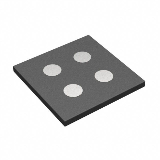
Unit: mm
0.80
3
1
2
0.80
4
TOP
Low Drain-source ON resistance:Rds(on) typ. = 68 mΩ (VGS = -2.5 V)
CSP (Chip Size Package)
RoHS compliant (EU RoHS / MSL:Level 1 compliant)
0.10
Features
0.40
Marking Symbol: 1D
BOTTOM
Packaging
Embossed type (Thermo-compression sealing) : 1 000 pcs / reel (standard)
Absolute Maximum Ratings Ta = 25 °C
Parameter
Symbol
Drain-Source Voltage
Gate-Source Voltage
Drain Current
Peak Drain Current
Power Dissipation
Channel Temperature
Operating Ambient Temperature
Storage Temperature
Note *1
*2
*3
*4
VDS
VGS
ID1*1
ID2*2
ID3*3
IDp1*1*4
IDp2*2*4
IDp3*3*4
PD1*1
PD2*2
PD3*3
Tch
Topr
Tstg
Rating
Unit
-12
±8
-2.2
-3.3
-4.1
-17
-26
-32
0.36
0.82
1.3
150
-40 ~ +85
-55 ~ +150
V
V
0.60
0.20
0.40
0.60
1. Gate
2. Drain
Panasonic
JEITA
Code
3. Source
4. Source
XLGA004-W-0808-RA01
—
—
Internal Connection
2(D)
A
A
W
°C
°C
°C
1(G)
3,4(S)
FR4 board (25.4mm×25.4mm×t1.0mm)、Min Cu 36mm2 Copper
FR4 board (25.4mm×25.4mm×t1.0mm)、Full Cu
Ceramic substrate (70mm×70mm×t1.0mm)
t = 10 μs, Duty Cycle < 1%
Page 1 of 6
�Product Standards
MOS FET
FJ4B01100L1
Electrical Characteristics Ta = 25 °C ± 3 °C
Parameter
Symbol
Drain-Source Breakdown Voltage
Zero Gate Voltage Drain Current
Gate-Source Leakage Current
Gate Threshold Voltage
VDSS
IDSS
IGSS
Vth
Drain-Source ON Resistance
RDS(on)
Input Capacitance *1
Output Capacitance *1
Reverse Transfer Capacitance *1
Turn-on delay time *1,*2
Rise time *1,*2
Turn-off delay time *1,*2
Fall time *1,*2
Total Gate Charge *1
Gate to Source Charge *1
Gate to Drain Miller Charge *1
Body Diode Forward Voltage
Ciss
Coss
Crss
td(on)
tr
td(off)
tf
Qg
Qgs
Qgd
VF(D-S)
Note
Conditions
ID = -1 mA, VGS = 0
VDS = -12 V, VGS = 0
VGS = ±8 V, VDS = 0 V
ID = -1.2 mA, VDS =-10 V
ID = -1.5 A, VGS = -4.5 V
ID = -1.5 A, VGS = -2.5 V
ID = -0.2 A, VGS = -1.8 V
ID = -0.1 A, VGS = -1.5 V
VDS = -10 V
VGS = 0
f = 1MHz
Min
Typ
Max
Unit
-12
-0.3
57
68
82
97
459
85
75
8
11
59
10
7
0.75
0.95
-0.7
VDD = -6 V
VGS = 0 to -4.5 V
ID = -1.0 A
VDD = -6 V
VGS = -4.5 V
ID = -1.0 A
IF = -0.2A, VGS = 0V
V
μA
μA
V
-10
±10
-1.0
74
90
139
290
mΩ
pF
ns
nC
nC
nC
V
-1.2
Measuring methods are based on JAPANESE INDUSTRIAL STANDARD JIS C 7030 Measuring methods for transistors.
*1 Guaranteed by design, not subject to production testing
*2 Measurement circuit for Turn-on delay time / Rise time / Turn-off delay time / Fall time
Electrical State Discharge Characteristics
Standard
Test Type
Symbol
Conditions
Human body model HBM C = 100 pF, R = 1.5 kΩ
AEC-Q101-001
C = 200 pF, R = 0 Ω
MM
Machine model
Class
Value
H1C >1k to ≦ 2k
M2 >100 to ≦ 200
Unit
V
V
Page 2 of 6
�Product Standards
MOS FET
FJ4B01100L1
Note2: Measurement circuit
VDD = -6V
Vin
0V
-4.5 V
PW = 10 μs
D.C. ≦ 1 %
RL = 6 Ω
ID = -1A
Vout
D
Vin
G
50 Ω
S
10 %
Vin
90 %
90 %
Vout
10 %
td(on) tr
td(off) tf
Page 3 of 6
�Product Standards
MOS FET
FJ4B01100L1
ID - VDS
RDS(on) - ID
-1.0
1000
Drain source On-resistance
RDS (on) (mΩ)
- 4.5 V
Drain current ID (A)
- 2.5 V
- 1.8 V
-0.5
- 1.5 V
VGS = - 1.2 V
-0.0
-0.0
-0.1
-0.2
100
-0.3
VGS = - 4.5 V
-0.1
-1.0
Drain current ID(A)
ID - VGS
Drain-source On-resistance
RDS(on) (mΩ)
Drain current ID (A)
125 ºC
85 ºC
25 ºC
-0.10
- 40 ºC
-0.01
-0.5
240
220
200
180
160
140
120
100
80
60
40
20
0
125 ºC
85 ºC
25 ºC
- 40 ºC
-0
-1.0
-1
-2
-3
-4
-5
-6
-7
-8
Gate-source voltage VGS ( V)
Gate-source voltage VGS (V)
IF - VF
IGS - VGS
-1.E-04
85 ºC
125 ºC
25 ºC
-0.10
- 40 ºC
-0.01
-0.2
-0.4
-0.6
-0.8
Body Diode Forward Voltage VF (V)
Gate-source Leakage Current
IGS (A)
-1.00
Diode Forward Current IF (A)
-10.0
RDS(on) - VGS
-1.00
-0.0
- 2.5 V
10
Drain-source voltage VDS (V)
-0.0
- 1.8 V
- 1.5 V
-1.0
125 ºC
-1.E-05
85 ºC
-1.E-06
25 ºC
-1.E-07
- 40 ºC
-1.E-08
-1.E-09
-0
-5
-10
-15
-20
Gate-source voltage VGS (V)
Page 4 of 6
�Product Standards
MOS FET
FJ4B01100L1
IDS - VDS
Dynamic Input/Output Characteristics
-4.5
Gate to source Voltage VG (V)
-1.E-04
125 ºC
-1.E-05
-1.E-06
-1.E-07
-1.E-08
-1.E-09
-40 ºC
-1.E-10
25 ºC
85 ºC
-1.E-11
-0
-4.0
-3.5
-3.0
VDD = - 6 V
-2.5
-2.0
- 12 V
-1.5
-1.0
-0.5
-0.0
0
-5
-10
-15
-20
-25
Drain-source Voltage VDS ( V )
1
2
3
4
5
6
7
Total Gate Charge Qg (nC)
Rth - tsw
Safe Operating Area
1000
-1.E+02
Min Cu 36mm2 Copper.
IDP=-17A
10us
Drain current ID (A)
Thermal resistance Rth (ºC / W)
Zero Gate Voltage Drain Current
IDS ( A )
-1.E-03
100
Full Cu
10
Ta=25ºC, Mounted on FR4 board
(25.4mm×25.4mm×t1.0mm).
Limited by
RDS(on)(VGS=-4.5V)
-1.E+00
1ms
10ms
-1.E-01
Ta=25ºC, Mounted on FR4 board
(25.4mm×25.4mm×t1.0mm).
Min Cu 36mm2 Copper.
100ms
1s
DC
-1.E-02
1
0.001
-1.E+01
0.1
10
Pulse Width (s)
1000
-1.E-02
-1.E-01
-1.E+00
-1.E+01
-1.E+02
Drain-source Voltage VDS (V)
Page 5 of 6
�Product Standards
MOS FET
FJ4B01100L1
XLGA004-W-0808-RA01
Unit: mm
0.80±0.04
3
1
2
0.10±0.02
0.80±0.04
4
0.60
0.40
Φ0.20±0.03
0.40
0.60
Land Pattern (Reference)
0.40
Φ0.20±0.03
0.40
Page 6 of 6
�
很抱歉,暂时无法提供与“FJ4B01100L1”相匹配的价格&库存,您可以联系我们找货
免费人工找货