物料型号:FK4B01120L1
器件简介:
- 这是一款用于负载开关电路的单N沟道MOSFET。
- 符合RoHS指令(欧盟RoHS / MSL:1级合规)。
- 低漏极-源极导通电阻:典型值为17毫欧(VGS = 2.5V)。
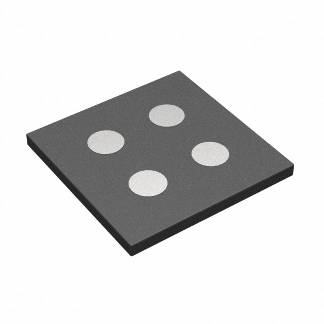
- 采用CSP(芯片尺寸封装)。
引脚分配:
- 1号引脚:栅极(Gate)
- 2号引脚:漏极(Drain)
- 3号和4号引脚:源极(Source)
参数特性:
- 漏极-源极电压(VDS):12V
- 栅极-源极电压(VGS):±8V
- 漏极电流(ID):ID1为3.9A,ID2为6.5A,ID3为7.9A
- 峰值漏极电流(IDp):IDp1为31A,IDp2为52A,IDp3为63A
- 功率耗散(PD):PD1为0.37W,PD2为0.94W,PD3为1.5W
- 通道温度(Tch):150℃
- 工作环境温度(Topr):-40℃至+85℃
- 存储温度(Tstg):-55℃至+150℃
功能详解:
- 该MOSFET具有低导通电阻和符合RoHS指令的特点,适用于负载开关电路。
- 电气特性包括漏极-源极击穿电压、栅极-源极漏电流、栅极阈值电压、输入电容、输出电容、反向传输电容、导通延迟时间、上升时间、关断延迟时间、下降时间、总栅极电荷、栅极到源极电荷、栅极到漏极米勒电荷、体二极管正向电压等。
应用信息:
- 适用于负载开关电路,具有低导通电阻和高效率。
封装信息:
- 封装类型:ULGA004-W-1010-RA01
- 封装尺寸:单位为毫米,具体尺寸信息在文档中有详细描述。