MN101C49 Series
MN101C49G
Type
Internal ROM type
MN101C49H
MN101CF49K
MN101CP49K
Mask ROM
MN101C49K
FLASH
EPROM
ROM (byte)
128K
160K
224K
RAM (byte)
4K
6K
10K
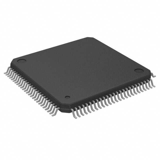
LQFP100-P-1414, QFP100-P-1818B
[Standard]
0.10 µs (at 4.5 V to 5.5 V, 20 MHz)
0.238 µs (at 2.7 V to 5.5 V, 8.39 MHz)
125 µs (at 2.0 V to 5.5 V, 32 kHz)*
[Double speed]
0.12 µs (at 4.5 V to 5.5 V, 8.39 MHz)
0.25 µs (at 3.0 V to 5.5 V, 4 MHz)
62.5 µs (at 2.0 V to 5.5 V, 32 kHz)*
*: The lower limit for operation guarantee for EPROM built-in type is 2.3 V.
The lower limit for operation guarantee for flash memory built-in type is 4.5 V.
Package (Lead-free)
Minimum Instruction
Execution Time
Interrupts
RESET. Watchdog. External 0 to 5. Timer 0 to 4. Timer 6. Timer 7 (2 systems). Time base. Serial 0 to 3. Automatic transfer finish. A/D
conversion finish. Key interrupts (8 lines)
Timer Counter
8-bit timer × 6
Timer 0 ..................Square-wave/8-bit PWM output. Event count. Remote control carrier output. Pulse width measurement
Timer 1 ..................Square-wave output. Event count. Synchronous output event
Timer 2 ..................Square-wave/8-bit PWM output. Event count. Synchronous output event. Pulse width measurement
Timer 3 ..................Square-wave output. Event count. Remote control carrier output
Timer 4 ..................Square-wave/8-bit PWM output. Event count. Pulse width measurement. Serial 1 baud rate timer
Timer 6 ..................8-bit freerun timer
Timer 0, 1 can be cascade-connected
Timer 2, 3 can be cascade-connected
16-bit timer × 1
Timer 7 ..................Square-wave/16-bit PWM output (cycle/duty continuous variable). Event count. Synchronous output event. Pulse
width measurement. Input capture
Time base timer: One-minute count setting
Watchdog timer × 1
Serial interface
Synchronous type/UART (full-duplex) × 1: Serial 0
Synchronous type/Simple UART (half-duplex) × 1: Serial 1
Synchronous type × 1: Serial 2
Synchronous type/Single-master I2C × 1: Serial 3
DMA controller
Maximum transfer cycles: 255
Starting factor: External request. Various types of interrupt. Software
Transfer mode: 1-byte transfer. Word transfer. Burst transfer
I/O Pins
I/O
Input
73 :
(72) :
15 :
(14) :
Common use. Specified pull-up resistor available. Input/output selectable (bit unit)
Flash memory built-in type
Common use. Specified pull-up resistor available
Flash memory built-in type
A/D converter
10-bit × 8 channels (with S/H)
D/A converter
8-bit × 4 channels
Special Ports
Buzzer output. Remote control carrier output. High-current drive port
MAD00011LEM
�MN101C49G, MN101C49H, MN101C49K, MN101CF49K, MN101CP49K
ROM Correction
Correcting address designation: Up to 3 addresses possible
Electrical Charactreistics (Supply current)
Parameter
Operating supply current
Supply current at HALT
Supply current at STOP
Symbol
Condition
min
Limit
typ
30
max
70
Unit
mA
IDD1
fosc = 20 MHz. VDD = 5 V
IDD2
fosc = 8.39 MHz. VDD = 5 V
15
30
mA
IDD3
fx = 32.768 kHz. VDD = 3 V
40
120
µA
IDD4
fx = 32 kHz. VDD = 3 V (5 V). Ta = 25 °C
IDD5
fx = 32.768 kHz. VDD = 3 V (5 V). Ta = 85 °C
IDD6
VDD = 5 V. Ta = 25 °C
IDD7
VDD = 5 V. Ta = 85 °C
5(13) 11(30)
µA
30(90)
µA
3
µA
60
µA
Note) ( ): Flash memory built-in type
Pin Assignment
75
74
73
72
71
70
69
68
67
66
65
64
63
62
61
60
59
58
57
56
55
54
53
52
51
P74, A12
P73, A11
P72, A10
P71, A9
P70, A8
P67, A7
P66, A6
P65, A5
P64, A4
P63, A3
P62, A2
P61, A1
P60, A0
P54, A17
P53, A16
P52, NCS
P51, NRE
P50, NWE
P47, KEY7
P46, KEY6
P45, KEY5
P44, KEY4
P43, KEY3
P42, KEY2
P41, KEY1
QFP100-P-1818B, LQFP100-P-1414
76
77
78
79
80
81
82
83
84
85
86
87
88
89
90
91
92
93
94
95
96
97
98
99
100
VREFAN0, PA0
AN1, PA1
AN2, PA2
AN3, PA3
AN4, PA4
AN5, PA5
AN6, PA6
AN7, PA7
VREF+
VDD
OSC2
OSC1
VSS
XI
XO
MMOD
SBO0, P00
SBI0, P01
SBT0, P02
SBO2, P03
SBI2, P04
SBT2, P05
NDK, BUZZER, P06
SYSCLK, P07
1
2
3
4
5
6
7
8
9
10
11
12
13
14
15
16
17
18
19
20
21
22
23
24
25
A13, P75
A14, P76
A15, P77
D0, LED0, P80
D1, LED1, P81
D2, LED2, P82
D3, LED3, P83
D4, LED4, P84
D5, LED5, P85
D6, LED6, P86
D7, LED7, P87
SDO0, PD0
SDO1, PD1
SDO2, PD2
SDO3, PD3
SDO4, PD4
SDO5, PD5
SDO6, PD6
SDO7, PD7
DAVSS
DA0, PC0
DA1, PC1
DA2, PC2
DA3, PC3
DAVDD
Note) ( ): Flash memory built-in type
MAD00011LEM
50
49
48
47
46
45
44
43
42
41
40
39
38
37
36
35
34
33
32
31
30
29
28
27
26
P40, KEY0
P37, NDKDMA
P36, NSTDMA
P35, NLDDMA, SCL, SBT3
P34, NBT, SBI3
P33, NBR, SDA, SBO3
P32, SBT1
P31, RXD1, SBI1
P30, TXD1, SBO1
P17(VPP)
P16, TM4IO
P15
P14, TM7IO
P13, TM3IO
P12, TM2IO
P11, TM1IO
P10, TM0IO, RMOUT
P27, NRST
P26(VDD2)
P25, IRQ5
P24, IRQ4
P23, IRQ3
P22, IRQ2
P21, IRQ1, SENS
P20, IRQ0
�Request for your special attention and precautions in using the technical information and
semiconductors described in this book
(1) If any of the products or technical information described in this book is to be exported or provided to non-residents, the laws and
regulations of the exporting country, especially, those with regard to security export control, must be observed.
(2) The technical information described in this book is intended only to show the main characteristics and application circuit examples
of the products. No license is granted in and to any intellectual property right or other right owned by Panasonic Corporation or any
other company. Therefore, no responsibility is assumed by our company as to the infringement upon any such right owned by any
other company which may arise as a result of the use of technical information described in this book.
(3) The products described in this book are intended to be used for standard applications or general electronic equipment (such as office
equipment, communications equipment, measuring instruments and household appliances).
Consult our sales staff in advance for information on the following applications:
– Special applications (such as for airplanes, aerospace, automobiles, traffic control equipment, combustion equipment, life support
systems and safety devices) in which exceptional quality and reliability are required, or if the failure or malfunction of the products may directly jeopardize life or harm the human body.
– Any applications other than the standard applications intended.
(4) The products and product specifications described in this book are subject to change without notice for modification and/or improvement. At the final stage of your design, purchasing, or use of the products, therefore, ask for the most up-to-date Product
Standards in advance to make sure that the latest specifications satisfy your requirements.
(5) When designing your equipment, comply with the range of absolute maximum rating and the guaranteed operating conditions
(operating power supply voltage and operating environment etc.). Especially, please be careful not to exceed the range of absolute
maximum rating on the transient state, such as power-on, power-off and mode-switching. Otherwise, we will not be liable for any
defect which may arise later in your equipment.
Even when the products are used within the guaranteed values, take into the consideration of incidence of break down and failure
mode, possible to occur to semiconductor products. Measures on the systems such as redundant design, arresting the spread of fire
or preventing glitch are recommended in order to prevent physical injury, fire, social damages, for example, by using the products.
(6) Comply with the instructions for use in order to prevent breakdown and characteristics change due to external factors (ESD, EOS,
thermal stress and mechanical stress) at the time of handling, mounting or at customer's process. When using products for which
damp-proof packing is required, satisfy the conditions, such as shelf life and the elapsed time since first opening the packages.
(7) This book may be not reprinted or reproduced whether wholly or partially, without the prior written permission of our company.
20080805
�