Product Standards
NN31001A
http://www.semicon.panasonic.co.jp/en/
7 A Synchronous DC-DC Step down Regulator,
Power Supply in Package
(VIN = 4.5 V to 28 V, VOUT = 0.6 V to 5.5 V)
FEATURES
DESCRIPTION
High-Speed Response DC-DC Step Down Regulator Circuit
that employs Hysteretic Control System
Built-in inductor and capacitors
Skip (discontinuous) Mode for high efficiency at light load
Maximum Output Current : 7 A
NN31001A is a synchronous DC-DC step down
regulator (1-ch), Power Supply in Package (PSiP), which
integrates a Controller IC that employs a hysteretic
control system, two Power MOSFETs, an Inductor and
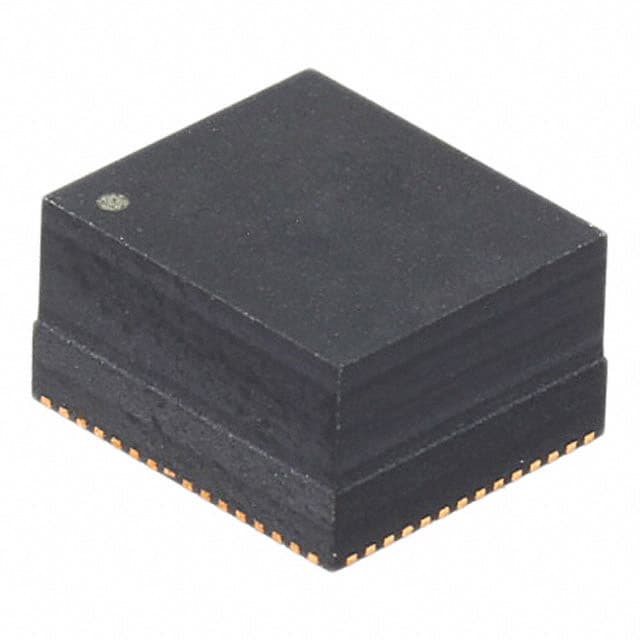
Capacitors into a single 8.5 x 7.5 x 4.7mm QFN package.
The easiness of mounting PSiP onto a Printed Circuit
Board (PCB), a very small footprint and a highly reduced
number of external components, offers very compact
and simplified solutions for applications requiring pointof-load design.
The number of external components have been reduced
to only input/output capacitor, slow start capacitor and
feedback resistors.
Furthermore, for applications requiring an output voltage
of 1.0 V / 3.3 V, the external feedback resistors can be
eliminated, resulting into even a smaller footprint.
The PSiP achieves efficiencies of greater than 94% with
very good power dissipation capabilities.
Input Voltage Range : PVIN=AVIN = 4.5 V to 28 V,
Output Voltage Range : 0.6 V to 5.5 V
Selectable Switching Frequency 400 kHz / 600 kHz / 800kHz
Built-in Feed Back Resistors for 1.0 V / 3.3 V default settings
Configurable output voltage settings using external Resistors
Adjustable Soft Start
Low Operating and Standby Quiescent Current
Open Drain Power Good Indication for Output Over / Under
Voltage
Selectable Auto recovery / latch off protection system
Adjustable current limit threshold
Built-in Under Voltage Lockout (UVLO),
Thermal Shut Down (TSD), Under Voltage Detection (UVD),
APPLICATIONS
Over Voltage Detection (OVD), Short Circuit Protection (SCP)
High Current Distributed Power Systems such as
Over Current Protection (OCP)
・DSP and FPGA Point-of-Load Applications
Plastic Quad Flat Non-leaded Package Heat Slug Down
・Routers
(QFN Type, Size : 8.5 mm 7.5 mm, 0.5 mm pitch)
・Industrial Equipment
・Space constrained Applications etc.
100
SIMPLIFIED APPLICATION
VREG
90
10uF x 2
PVIN
EN
PGOOD
AVIN
PRTCNT
BST
LX
OCPCNT
NN31001A
1k
Efficiency [%]
VIN
100k
VREG
MODE
FSEL
VFB
VOUTM
#1.0V / 3.3 V
without using FB resistor
VOUT
AGND1, 2
PGND
70
VOUT=1V, Fsw=400kHz
60
VOUT=1V, Fsw=600kHz
VOUT = 1.0V
1.5k
SS
80
22uF x 3
4.7nF
Note : The application circuit is an example. The operation of
the mass production set is not guaranteed. Sufficient
evaluation and verification is required in the design of
the mass production set. The Customer is fully
responsible for the incorporation of the above
illustrated application circuit in the design of the
equipment.
VOUT=1V, Fsw=800kHz
50
VOUT=3.3V, Fsw=600kHz
VOUT=3.3V, Fsw=800kHz
40
0.01
0.1
1
7 10
IOUT [A]
Condition :
Vin = 12 V, VOUT Setting = 1.0 V / 3.3 V
Switching Frequency = 400 / 600 / 800 kHz, Skip mode
Cout = 66 F ( 22 F x 3 )
Page 1 of 33
�Product Standards
NN31001A
ORDERING INFORMATION
Order Number
Feature
Package
Output Supply
NN31001A-BB
Maximum Output Current : 7 A
57 pin HQFN
Emboss Taping
ABSOLUTE MAXIMUM RATINGS
Parameter
Symbol
Rating
Unit
Notes
Supply voltage
VIN
30
V
*1
Operating free-air temperature
Topr
– 40 to + 85
C
*2
Operating junction temperature
Tj
– 40 to + 150
C
*2
Storage temperature
Tstg
– 55 to + 150
C
*2
– 0.3 to (VREG + 0.3)
V
Input Voltage Range
VMODE,VFSEL,VOUTM,VPRTCNT
VOCPCNT,VFB
*1
*3
VEN
– 0.3 to 6.0
V
*1
VPGOOD
– 0.3 to (VREG + 0.3)
V
*1
*3
VLX
– 0.3 to (VIN + 0.3)
V
*1
*4
HBM
2
kV
—
Output Voltage Range
ESD
Notes : This product may sustain permanent damage if subjected to conditions higher than the above stated absolute
maximum rating. This rating is the maximum rating and device operating at this range is not guaranteed as it
is higher than our stated recommended operating range.
When subjected under the absolute maximum rating for a long time, the reliability of the product may be affected.
VIN is voltage for AVIN, PVIN. VIN = AVIN = PVIN.
Do not apply external currents and voltages to any pin not specifically mentioned.
*1 : The values under the condition not exceeding the above absolute maximum ratings and
the power dissipation.
*2 : Except for the power dissipation, operating ambient temperature, and storage temperature,
all ratings are for Ta = 25 C.
*3 :(VREG + 0.3) V must not exceed 6 V.
*4 : (VIN + 0.3) V must not exceed 30 V.
Page 2 of 33
�Product Standards
NN31001A
POWER DISSIPATION RATING
Package
Plastic Quad Flat Non-leaded Package
Heat Slug Down (QFN Type)
j-C
PD
(Ta = 25 C)
PD
(Ta = 85 C)
Notes
6.7 C / W
3.49 W
1.82 W
*1
5.7 C / W
5.56 W
2.89 W
*2
Notes : For the actual usage, please follow the power supply voltage, load and ambient temperature conditions to ensure that there is
enough margin and the thermal design does not exceed the allowable value.
*1:Glass Epoxy Substrate (4 Layers) [50 50 0.8 t (mm)]
*2:Glass Epoxy Substrate (4 Layers) [50 50 1.57 t (mm)]
CAUTION
Although this IC has built-in ESD protection circuit, it may still sustain permanent damage if not handled
properly. Therefore, proper ESD precautions are recommended to avoid electrostatic damage to the MOS
gates.
RECOMMENDED OPERATING CONDITIONS
Parameter
Supply voltage range
Input Voltage Range
Output Voltage Range
Symbol
Min
Typ
Max
Unit
Notes
AVIN
4.5
12
28
V
—
PVIN
4.5
12
28
V
—
VMODE
– 0.3
—
VREG + 0.3
V
*1
VFSEL
– 0.3
—
VREG + 0.3
V
*1
VPRTCNT
– 0.3
—
VREG + 0.3
V
*1
VEN
– 0.3
—
5.0
V
—
VPGOOD
– 0.3
—
VREG + 0.3
V
*1
VLX
– 0.3
—
VIN + 0.3
V
*2
Notes : Voltage values, unless otherwise specified, are with respect to GND.
GND is voltage for AGND, PGND. AGND = PGND
VIN is voltage for AVIN, PVIN. VIN = AVIN = PVIN.
Do not apply external currents or voltages to any pin not specifically mentioned.
*1 : (VREG + 0.3) V must not exceed 6 V.
*2 : (VIN + 0.3) V must not exceed 30 V.
Page 3 of 33
�Product Standards
NN31001A
ELECTRICAL CHARACTERISTICS
CO = 22 µF 3, VOUT Setting = 1.0 V, VIN = AVIN = PVIN = 12 V, Switching Frequency = 600 kHz
VMODE = VREG (FCCM), Ta = 25 C 2 C unless otherwise noted.
Parameter
Symbol
Condition
Limits
Unit Note
Min
Typ
Max
IVDDACTN1
IOUT = 0 A, VFB = 0.620 V
RFB1 = 1.0 k
RFB2 = 1.5 k
VMODE = 0 V, VEN = 5 V
—
700
1200
µA
—
IVDDACTN2
VEN = 5 V , IOUT = 0 A
RFB1 = 1.0 k
RFB2 = 1.5 k
VMODE = VREG
VFSEL = OPEN
—
15
23
mA
—
AVIN = PVIN = 12 V
VEN = 0 V
—
2
5
µA
—
Current Consumption
Current Consumption at active1
(Skip mode)
Current Consumption at active2
(FCCM)
AVIN/PVIN Current Consumption
at standby
IVINSTB
Logic Pin Characteristics
EN pin Low-level input voltage
VENL
—
—
—
0.3
V
—
EN pin High-level input voltage
VENH
—
1.5
—
5.0
V
—
—
10
20
µA
—
EN pin leakage current
ILEAKEN
MODE pin Low-level input voltage
VMODEL
—
—
—
VREG
0.3
V
—
MODE pin High-level input voltage
VMODEH
—
VREG
0.7
—
VREG
V
—
MODE pin leakage current
ILEAKMD
—
12.5
25
µA
—
VEN = 5 V
VMODE = 5 V
PRTCNT pin Low-level input
voltage
VPRTL
—
—
—
0.3
V
—
PRTCNT pin High-level input
voltage
VPRTH
—
VREG
– 0.3
—
—
V
—
PRTCNT pin leakage current
ILEAKPRT
VEN = 5 V, VPRTCNT = 5 V
—
0
2
µA
—
FSEL pin Low-level input voltage
VFSELL
—
—
—
0.3
V
—
FSEL pin High-level input voltage
VFSELH
—
VREG
– 0.3
—
—
V
—
FSEL pin High leakage current
ILEAKFSH
VFSEL = 5 V
—
6.25
12.5
µA
—
FSEL pin Low leakage current
ILEAKFSL
VFSEL = 0 V
—
6.25
12.5
µA
—
Page 4 of 33
�Product Standards
NN31001A
ELECTRICAL CHARACTERISTICS (Continued)
CO = 22 µF 3, VOUT Setting = 1.0 V, VIN = AVIN = PVIN = 12 V, Switching Frequency = 600 kHz
VMODE = VREG (FCCM), Ta = 25 C 2 C unless otherwise noted.
Parameter
Symbol
Condition
Limits
Min
Typ
Max
Unit Note
VREG Characteristics
Output voltage
VREGO
IVREG = 5mA
5.3
5.6
5.9
V
—
Input voltage variation
VREGLIN
VREGLIN = VREG (VIN =12 V)
-VREG (VIN =6 V)
IVREG = 5mA
—
—
150
mV
—
Drop out voltage
VREGDO
VIN = 4.5 V, IVREG = 5mA
4.1
—
—
V
—
0.594
0.600
0.606
V
—
VFB Characteristics
VFB comparator threshold
VFBTH
VFB pin leakage current 1
ILEAKFB1
VFB = 0 V
–1
—
1
µA
—
VFB pin leakage current 2
ILEAKFB2
VFB = 6 V
–1
—
1
µA
—
UVLO shutdown voltage
VUVLODE
VIN = 5 V to 0 V
3.97
4.10
4.23
V
—
UVLO wakeup voltage
VUVLORE
VIN = 0 V to 5 V
4.17
4.30
4.43
V
—
UVLO hysteresis
VUVLO
150
200
250
mV
—
—
Under Voltage Lock Out
—
PGOOD
PGOOD Threshold 1
(VFB ratio for UVD detect)
PGOOD Hysteresis 1
(VFB ratio for UVD release)
PGOOD Threshold 2
(VFB ratio for OVD detect)
PGOOD Hysteresis 2
(VFB ratio for OVD release)
VPGUV
PGOOD : High to Low
77
85
93
%
—
VPGUV
PGOOD : Low to High
3.5
5.0
6.5
%
—
VPGOV
PGOOD : High to Low
107
115
123
%
—
VPGOV
PGOOD : Low to High
3.5
5.0
6.5
%
—
PGOOD start up delay time
( After reached VFB = 0.6 V )
TPGD
—
0.4
1.0
1.6
ms
—
PGOOD ON resistance
RPG
—
—
10
15
—
Page 5 of 33
�Product Standards
NN31001A
ELECTRICAL CHARACTERISTICS (Continued)
CO = 22 µF 3, VOUT Setting = 1.0 V, VIN = AVIN = PVIN = 12 V, Switching Frequency = 600 kHz
VMODE = VREG (FCCM), Ta = 25 C 2 C unless otherwise noted.
Parameter
Symbol
Condition
Limits
Unit Note
Min
Typ
Max
Vo1
RFB1 = 1.0 k
RFB2 = 1.5 k
VMODE = VREG
IOUT = 3.5 A
0.985
1.000
1.015
V
—
Vo2
RFB1 = 4.5 k
RFB2 = 1 k
VMODE = VREG
IOUT = 3.5 A
3.250
3.300
3.350
V
—
Vo3
VFB = OPEN
before VEN = 0 V to 1.5 V
VMODE = VREG
IOUT = 3.5 A
0.985
1.000
1.015
V
—
Vo4
VFB = VREG
before VEN = 0 V to 1.5 V
VMODE = VREG
IOUT = 3.5 A
3.250
3.300
3.350
V
—
Efficiency 1
VEFF1
PVIN = 12 V
VOUT = 5 V, IOUT = 4 A
VFSEL = VREG ( 800kHz )
—
95
—
%
*1
Efficiency 2
VEFF2
PVIN = 12 V
VOUT = 3.3 V, IOUT = 4 A
VFSEL = OPEN ( 600kHz )
—
95
—
%
*1
Efficiency 3
VEFF3
PVIN = 12 V
VOUT = 3.3 V, IOUT = 4 A
VFSEL = VREG ( 800kHz )
—
94
—
%
*1
Efficiency 4
VEFF4
PVIN = 12 V
VOUT = 1.0 V, IOUT = 4 A
VFSEL = 0 V ( 400kHz )
—
88
—
%
*1
Efficiency 5
VEFF5
PVIN = 12 V
VOUT = 1.0 V, IOUT = 4 A
VFSEL = OPEN ( 600kHz )
—
87
—
%
*1
Efficiency 6
VEFF6
PVIN = 12 V
VOUT = 1.0 V, IOUT = 4 A
VFSEL = VREG ( 800kHz )
—
85
—
%
*1
DC-DC Characteristics
Output voltage 1
Output voltage 2
Output voltage 3
Output voltage 4
Note :
*1 : Typical design value
Page 6 of 33
�Product Standards
NN31001A
ELECTRICAL CHARACTERISTICS (Continued)
CO = 22 µF 3, VOUT Setting = 1.0 V, VIN = AVIN = PVIN = 12 V, Switching Frequency = 600 kHz
VMODE = VREG (FCCM), Ta = 25 C 2 C unless otherwise noted.
Parameter
Symbol
Condition
Limits
Min
Typ
Max
Unit Note
DC-DC Characteristics
Note :
Load regulation1
VLOA1
IOUT = 10 mA to 7 A
VMODE = 0 V
—
2.0
—
%
*1
Load regulation2
VLOA2
IOUT = 10 mA to 7 A
VMODE = VREG
—
1.0
—
%
*1
Line regulation
VLIN
PVIN = 6 V to 28 V
VMODE = VREG
IOUT = 2.0 A
—
0.1
0.3
%/V
—
Output ripple voltage 1
VRL1
IOUT = 10 mA
VMODE = 0 V
—
30
—
mV
[p-p]
*1
Output ripple voltage 2
VRL2
IOUT = 10 mA
VMODE = VREG
—
15
—
mV
[p-p]
*1
Output ripple voltage 3
VRL3
IOUT = 3.5 A
VMODE = VREG
—
10
—
mV
[p-p]
*1
Load transient response 1
VTR1
IOUT = 100 mA to 3.5 A
t = 0.5 A / µs
VMODE = 0 V or VREG
—
15
—
mV
*1
Load transient response 2
VTR2
IOUT = 3.5 A to 100 mA
t = 0.5 A / µs
VMODE = 0 V or VREG
—
20
—
mV
*1
Minimum Input and output voltage
difference
VDIFF
VDIFF = VIN – VOUT
—
2.5
—
V
*1
*1 : Typical design value
Page 7 of 33
�Product Standards
NN31001A
ELECTRICAL CHARACTERISTICS (Continued)
CO = 22 µF 3, VOUT Setting = 1.0 V, VIN = AVIN = PVIN = 12 V, Switching Frequency = 600 kHz
VMODE = VREG (FCCM), Ta = 25 C 2 C unless otherwise noted.
Parameter
Symbol
Condition
Limits
Min
Typ
Max
Unit Note
Protection
DC-DC Over Current
Protection Limit 1
ILMT1
OCPCNT=OPEN
—
9.0
—
A
*1
DC-DC Over Current
Protection Limit 2
ILMT2
OCPCNT=220 k
—
7.0
—
A
*1
DC-DC Over Current
Protection Limit 3
ILMT3
OCPCNT=100 k
—
4.7
—
A
*1
Thermal Shut Down (TSD)
Threshold
TTSDTH
—
—
130
—
C
*1
Thermal Shut Down (TSD)
Hysteresis
TTSDHYS
—
—
30
—
C
*1
Soft-Start Timing
SS Charge Current
ISSCHG
VSS = 0.3 V
1
2
4
µA
—
SS Discharge Resistance (Shut-down)
RSSDIS
VEN = 0 V
—
5
10
k
—
Switching Frequency Adjustment
DC-DC Switching Frequency 1
FSW1
IOUT = 4 A, VFSEL = 0 V
—
400
—
kHz
*1
DC-DC Switching Frequency 2
FSW2
IOUT = 4 A, VFSEL = OPEN
—
600
—
kHz
*1
DC-DC Switching Frequency 3
FSW3
IOUT = 4 A, VFSEL = VREG
—
800
—
kHz
*1
Note :
*1 : Typical design value
Page 8 of 33
�Product Standards
NN31001A
PIN CONFIGURATION
30 31 32
LX
PVIN
VFB
SS
PGOOD
OCPCNT
PRTCNT
VREG
FSEL
MODE
EN
AGND
39 40 41 42 43
62 AGND
61
LX
58
VOUT
59
PGND
60
PVIN
PVIN
15 14 13 12 11 10 9 8
44
45
46
47
48
49
50
51
52
53
54
55
56
57
VFB
AGND
VOUTM
PGND
VOUT
7 6 5 4 3 2 1
VOUT
LX_S
29
28
27
26
25
24
23
22
21
20
19
18
17
16
33 34 35 36 37 38
PGND
BST
AVIN
N.C.
AGND
BST
Bottom View
PIN FUNCTIONS
Pin No.
Pin name
Type
VOUT
Output
Description
1
2
3
48
49
50
51
Output voltage pin
52
53
54
55
56
57
Note : Detailed pin descriptions are provided in the OPERATION and APPLICATION INFORMATION section.
Page 9 of 33
�Product Standards
NN31001A
PIN FUNCTIONS (Continued)
Pin No.
Pin name
Type
Description
PGND
Ground
Ground pin for Power MOSFET
* Pin No. 47 : recommended settings – no connection
PVIN
Power
supply
Power supply pin for Power MOSFET
Recommended rise time ( time to reach 90 % of set value ) setting is
greater than or equal to 10 µs and less than or equal to 1 s.
4
5
6
7
47
8
9
10
11
12
13
14
15
16
17
18
19
20
21
22
LX
Output
23
Power MOSFET output pin
An inductor is connected and switching operation is carried out
between VIN and GND.
* Pin No. 19 to 25 : recommended settings – no connection
24
25
26
Output
Power MOSFET output sense pin
* Pin No. 26 to 27 : recommended settings – no connection
BST
Output
High side Power MOSFET gate driver pin
Bootstrap operation is carried out in order to drive the gate voltage of High
side Power MOSFET.
* Pin No. 28 to 30 : recommended settings – no connection
NC
-
AGND
Ground
33
AVIN
Power supply
34
EN
Input
27
LX_S
28
29
30
31
Non Connection pin
32
39
Ground pin
45
Power supply pin
Recommended rise time ( time to reach 90 % of set value ) setting is
greater than or equal to 10 µs and less than or equal to 1 s.
ON / OFF control pin
DC-DC is stopped at Low level input, and it is started at High level input.
Note : Detailed pin descriptions are provided in the OPERATION and APPLICATION INFORMATION section.
Page 10 of 33
�Product Standards
NN31001A
PIN FUNCTIONS (Continued)
Pin No.
Pin name
Type
35
FSEL
Input
Frequency select pin
This is set to 400 kHz at Low level input, 800 kHz at High level input,
and 600 kHz at open.
36
MODE
Input
Skip (discontinuous) mode / FCCM (Forced Continuous Conduction Mode)
select pin
Skip mode is set at Low level input, FCCM is set at High level input.
37
PRTCNT
Input
Protection Control Set pin for Latch mode / Auto recovery mode during
OVD / SCP operations
38
VREG
Output
40
OCPCNT
Input
41
42
PGOOD
SS
LDO output pin
This is Output pin of Power supply (LDO) for internal control circuit.
Programmable over-current protection. Connected resistor on this pin will
adjust the over-current protection threshold.
Output
Power good open drain pin
A pull up resistor between PGOOD and VREG terminal is necessary.
Output is low during Over or Under Voltage Detection conditions.
Output
Soft start capacitor connect pin
The output voltage at a start up is smoothly controlled
by adjusting Soft Start time.
Please connect capacitor between SS and GND.
Input
Comparator negative input pin / 1.0 V, 3.3 V output voltage select pin
VFB terminal voltage is regulated to REF output (internal reference voltage).
Since VFB is a high impedance terminal, it should not be routed near
other noisy path (LX, BST, etc.)
Routing path should be kept as short as possible.
Output voltage sense pin
Switching frequency is controlled by monitoring output voltage.
This pin is also used as Feedback pin during internal feedback function.
43
VFB
Description
44
46
VOUTM
Input
58
VOUT
Output
Voltage output pin for heat radiation
59
PGND
Ground
Ground pin of Power MOSFET for heat radiation
60
PVIN
Power
supply
Power supply pin for heat radiation
61
LX
Output
Power MOSFET output pin for heat radiation
62
AGND
Ground
Ground pin for heat radiation
Note : Detailed pin descriptions are provided in the OPERATION and APPLICATION INFORMATION section.
Page 11 of 33
�Product Standards
NN31001A
FUNCTIONAL BLOCK DIAGRAM
AVIN
SS
33
42
EN
34
VBG
BGR
VINT
SS
Soft-Start
41
PGOOD
0.6 V + 15 %
VREG
38
VREG
5.6 V
For internal power
0.6 V – 15 %
8, 9, 10
11, 12, 13
14, 15, 16
17, 18, 60
VREG
UVLO
For internal reset release
OCP
UVLO
PVIN
TSD
SCP
VOUTM
46
1.0V / 3.3V
Divider/Selector
28, 29, 30 BST
Fault
HPD
HGATE
19, 20, 21
22, 23, 24
25, 61
LX
43, 44
VFB
Soft Start
VREG
FSEL
35
AVIN
36
MODE
VREF
Ton
Timer + Comp
OCPCNT
40
26, 27 LX_S
HGO
Lo
0.6 V
Toff
Timer + Comp
VOUT
ON
CMP
1, 2, 3
48, 49, 50
51, 52, 53
54, 55, 56
57, 58
LGATE
Control
Logic
LPD
PGND
LGO
FCCM
/ Skip
37
PRTCNT
REF
4, 5, 6
7, 47, 59
Protect
control
OCP
threshold
control
32, 39, 45, 62
AGND
31
N.C.
Note : This block diagram is for explaining functions. Part of the block diagram may be omitted, or it may be simplified.
Page 12 of 33
�Product Standards
NN31001A
OPERATION
1. Protection
(1) Output Over-Current Protection (OCP) function
And Short-Circuit Protection (SCP) function
1) The Over Current Protection is activated at about
9 A (Typ.) when OCPCNT pin is set to open. This
device uses pulse – by – pulse valley current
protection method. When the low side MOSFET is
turned on, the voltage across the drain and source is
monitored which is proportional to the inductor current.
The high side MOSFET is only allowed to turn on when
the current flowing in the low side MOSFET falls below
the OCP level. Hence, during the OCP, the output
voltage continues to drop at the specified current.
Output Voltage [V]
Over Current Protection ( typ : 9 A )
#OCPCNT = OPEN
7.3 A to 10.7 A
1)
2)
(Ground short
protection Detection
about 60 % of Vout )
3) The Short-Circuit Protection function is implemented
when the output voltage decreases and the VFB pin
reaches to about 60 % of the set voltage of 0.6 V. If the
VFB voltage stays below 70 % of 0.6 V for more than
250 µs after SCP triggers, both high side and low side
MOSFET will be turned off and the output will be
discharged by internal MOS transistor.
(The above operation after SCP triggered is at latch off
mode. The details are described in the next page)
(2) Output Over Voltage Detection
If the VFB pin voltage exceeds 115 % of a
predetermined value (0.6 V) and lasts more than 10ns,
overvoltage detection will be triggered and PGOOD pin
will be pulled down. Furthermore, in an overvoltage
condition, high side and low side MOSFETs are turned
off to stop PWM operation. If the VFB pin voltage drops
below 110 % of the predetermined value (0.6 V) within
2 ms after overvoltage detection triggers, PGOOD pin
will be pulled up again and PWM operation will resume.
Otherwise, IC is transferred to latch off state and the
output will be discharged by internal MOS transistor.
(The above operation after OVD triggered is at latch off
mode. The details are described in the next page)
VFB
Output current [A]
Figure : OCP and SCP Operation
Note: PRTCNT = VREG ( SCP latch off mode )
2) The Over Current Protection threshold level can be
programmed by connecting a pull down resistor at
OCPCNT pin. The value of the resistor connected
between OCPCNT pin and ground will determine the
OCP threshold level.
115 %
110 %
100 %
0.6 V
0.6 V
2 ms
PGOOD
1 ms
Note: The OCP level is fixed to around 0.7 A when OCPCNT
pin is connected to Ground.
OCP level ( typ )
OCPCNT resistor
9A
OPEN ( more than 1M )
7A
220 k
4.7 A
100 k
Table : OCP threshold level
The accuracy of OCP level is around 20 % of the
typical value in the above table.
OCP level with resistor at OCPCNT pin ( ROCP ) can be
calculated by the following approximate equation.
OCP levelA 9
435
ROCP k
Figure : OVD Operation
Note: PRTCNT = VREG ( OVD latch off mode )
(3) Output discharging function
When EN is low, the output is discharged by an internal
MOSFET transistor.
When EN is high, if the controller is turned off either by
Under Voltage Lock Out (UVLO), Over Voltage
Detection (OVD) or Short Circuit Protection (SCP), the
output is discharged by an internal MOSFET transistor.
The ON-resistance of the internal MOSFET transistor
is about 35 .
Note: ROCP is recommended to be more than 100 k.
Page 13 of 33
�Product Standards
NN31001A
OPERATION (Continued)
1. Protection (Continued)
(4) Protection control (PRTCNT) function
The IC turn-off operation after Over Voltage Detection
and Short Circuit Protection can be programmed by
PRTCNT pin voltage. Changing the input level of
PRTCNT will select Latch off and Auto recovery mode
for OVD and SCP operations. The following table and
figures represents detailed explanation of this function.
After latch off detection, power reset or EN pin reset is
necessary to activate the device again.
VFB
2ms
2 ms
DCDC
state
DCDC
state
ON
1 ms
1 ms
PGOOD
ON
OFF
( Latch off )
Figure : SCP Operation2
PRTCNT = VREG : Latch off case
Figure : OVD Operation1
PRTCNT = L : Auto recovery case
VFB
115 %
110 %
100 %
Switching
stop
Switching
stop
Switching
0.6 V
0.6 V
2 ms