Phototransistors
PNZ1270
Silicon NPN Phototransistor
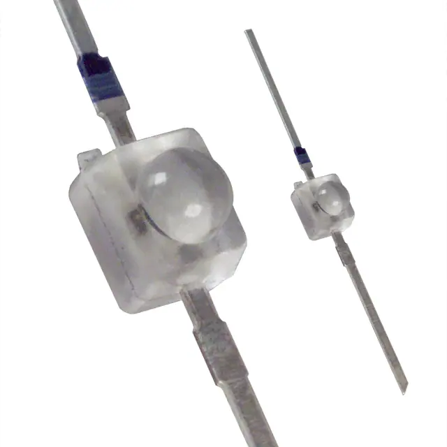
Unit : mm
For optical control systems
ø1.8
M
Di ain
sc te
on na
tin nc
ue e/
d
0.5±0.1
Features
Type number : Emitter mark (Blue)
10.0 min.
10.0 min.
3.2±0.3 3.2±0.3
High sensitivity
di
p
Pl
lan nclu
ea
e
se
pla m d m des
ne ain ain foll
htt visit
d te t o
p:/ fo
/w llo dis disc nan enan wing
ww wi co on ce c fo
.se ng ntin tin ty e ty ur
mi UR ue ued pe pe Pro
co L a d t ty
du
n.p bo yp pe
ct
life
an ut e
d
as lat
cy
on es
cle
ic. t in
sta
co fo
ge
.jp rm
.
/en at
i
o
/
n.
0.15
R0.9
0.85 ± 0.15
2.8±0.2
Small size designed for easier mounting to printed circuit board
Absolute Maximum Ratings (Ta = 25˚C)
Parameter
Symbol
Collector to emitter voltage
VCEO
Emitter to collector voltage
VECO
Collector current
IC
Collector power dissipation
PC
Operating ambient temperature
Topr
Storage temperature
Tstg
0.4±0.1
2.8±0.2 1.8
1.05±0.1
Fast response : tr = 2.5 µs (typ.)
1.8
2
2.2±0.15
(0.7)
45
˚
Good collector photo current linearity with respect to optical
power input
(0.7)
1
Ratings
Unit
20
V
5
V
20
mA
50
mW
–25 to +85
˚C
–30 to +100
˚C
1: Collector
2: Emitter
ue
Electro-Optical Characteristics (Ta = 25˚C)
Symbol
ICEO
Collector photo current
Peak sensitivity wavelength
*2
en
int
ICE(L)*3
VCE = 10V, L = 1000 lx*1
VCE = 10V
θ
Measured from the optical axis to the half power point
tr*2
tf*2
min
VCE = 10V
λP
Ma
Fall time
*1
an
Acceptance half angle
Rise time
Conditions
ce
/D
isc
on
tin
Parameter
Dark current
typ
max
1
100
nA
19.2
mA
0.8
VCC = 10V, ICE(L) = 1mA, RL = 100Ω
Unit
800
nm
14
deg.
2.5
µs
3.5
µs
Measurements were made using a tungsten lamp (color temperature T = 2856K) as a light source.
Switching time measurement circuit
Sig.IN
VCC
(Input pulse)
Sig.OUT (Output pulse)
RL
,,,,
,,
50Ω
*3 I
CE(L)
90%
10%
td
tr
tf
td : Delay time
tr : Rise time (Time required for the collector photo current to
increase from 10% to 90% of its final value)
tf : Fall time (Time required for the collector photo current to
decrease from 90% to 10% of its initial value)
Classifications
Class
Q
R
S
T
ICE(L) (mA)
0.8 to 2.4
1.6 to 4.8
3.2 to 9.6
6.4 to 19.2
1
�Phototransistors
PNZ1270
PC — Ta
ICE(L) — VCE
40
Ta = 25˚C
T = 2856K
L =1000 lx
4
3
Collector photo current
50
ICE(L) — L
10 5
ICE(L) (µA)
ICE(L) (mA)
5
VCE = 10V
Ta = 25˚C
T = 2856K
10 4
30
20
10
20
40
60
80
4
8
12
16
10 3
10 2
20
10
10
24
VCE (V)
ICE(L) — Ta
10 5
ICE(L) (mA)
VCE = 10V
10 2
Collector photo current
ICEO (nA)
10
1
10 2
Illuminance
10 3
10 4
L (lx)
Spectral sensitivity characteristics
100
VCE = 10V
T = 2856K
10 4
10 3
VCE = 10V
Ta = 25˚C
80
60
40
20
40
Ambient temperature
80
10 2
– 40
120
Ta (˚C )
an
Directivity characteristics
10˚
20˚
int
100
50
40
30
20
80
Ambient temperature
40˚
50˚
60˚
70˚
0
200
120
Ta (˚C )
tr — ICE(L)
400
600
800
1000
10
tf — ICE(L)
VCE = 10V
Ta = 25˚C
10
RL = 1kΩ
500Ω
1
100Ω
10 –1
1200
Wavelength λ (nm)
10 2
VCE = 10V
Ta = 25˚C
tr (µs)
60
30˚
Rise time
70
Relative sensitivity S (%)
Ma
90
80
40
10 2
en
0˚
0
RL = 1kΩ
tf (µs)
0
Fall time
10 –1
– 40
ce
/D
isc
on
tin
ue
Dark current
0
Collector to emitter voltage
ICEO — Ta
10 3
100 lx
0
100
Ta (˚C )
250 lx
1
S (%)
0
Ambient temperature
2
Relative sensitivity
0
– 20
500 lx
di
p
Pl
lan nclu
ea
e
se
pla m d m des
ne ain ain foll
htt visit
d te t o
p:/ fo
/w llo dis disc nan enan wing
ww wi co on ce c fo
.se ng ntin tin ty e ty ur
mi UR ue ued pe pe Pro
co L a d t ty
du
n.p bo yp pe
ct
life
an ut e
d
as lat
cy
on es
cle
ic. t in
sta
co fo
ge
.jp rm
.
/en at
i
o
/
n.
Collector photo current
M
Di ain
sc te
on na
tin nc
ue e/
d
Collector power dissipation
PC (mW)
60
500Ω
100Ω
1
10 –1
80˚
90˚
10 –2
10 –2
10 –1
Collector photo current
2
1
10
ICE(L) (mA)
10 –2
10 –2
10 –1
Collector photo current
1
10
ICE(L) (mA)
�Request for your special attention and precautions in using the technical information and
semiconductors described in this book
(1) If any of the products or technical information described in this book is to be exported or provided to non-residents, the laws and
regulations of the exporting country, especially, those with regard to security export control, must be observed.
(2) The technical information described in this book is intended only to show the main characteristics and application circuit examples
of the products, and no license is granted under any intellectual property right or other right owned by our company or any other
company. Therefore, no responsibility is assumed by our company as to the infringement upon any such right owned by any other
company which may arise as a result of the use of technical information described in this book.
M
Di ain
sc te
on na
tin nc
ue e/
d
(3) The products described in this book are intended to be used for standard applications or general electronic equipment (such as office
equipment, communications equipment, measuring instruments and household appliances).
Consult our sales staff in advance for information on the following applications:
– Special applications (such as for airplanes, aerospace, automobiles, traffic control equipment, combustion equipment, life support
systems and safety devices) in which exceptional quality and reliability are required, or if the failure or malfunction of the products may directly jeopardize life or harm the human body.
– Any applications other than the standard applications intended.
d
pla inc
ne lud
se
pla m d m es
v
ne ain ain foll
htt isit
d te t o
p:/ fo
/w llo dis disc nan enan wing
ww wi co on ce c fo
.se ng ntin tin ty e ty ur
mi UR ue ued pe pe Pro
co L a d t ty
du
n.p bo yp pe
ct
life
an ut e
d
as lat
cy
on es
cle
ic. t in
sta
co fo
ge
.jp rm
.
/en at
i
o
/
n.
(4) The products and product specifications described in this book are subject to change without notice for modification and/or improvement. At the final stage of your design, purchasing, or use of the products, therefore, ask for the most up-to-date Product
Standards in advance to make sure that the latest specifications satisfy your requirements.
(5) When designing your equipment, comply with the range of absolute maximum rating and the guaranteed operating conditions
(operating power supply voltage and operating environment etc.). Especially, please be careful not to exceed the range of absolute
maximum rating on the transient state, such as power-on, power-off and mode-switching. Otherwise, we will not be liable for any
defect which may arise later in your equipment.
Even when the products are used within the guaranteed values, take into the consideration of incidence of break down and failure
mode, possible to occur to semiconductor products. Measures on the systems such as redundant design, arresting the spread of fire
or preventing glitch are recommended in order to prevent physical injury, fire, social damages, for example, by using the products.
(6) Comply with the instructions for use in order to prevent breakdown and characteristics change due to external factors (ESD, EOS,
thermal stress and mechanical stress) at the time of handling, mounting or at customer's process. When using products for which
damp-proof packing is required, satisfy the conditions, such as shelf life and the elapsed time since first opening the packages.
Pl
ea
Ma
int
en
an
ce
/D
isc
on
tin
ue
(7) This book may be not reprinted or reproduced whether wholly or partially, without the prior written permission of Matsushita
Electric Industrial Co., Ltd.
�