TK
4 mm height!
2 A high capacity
1 Form C type ultra thin,
super miniature relay
FEATURES
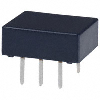
1. Compact and flat type
10.6(L) × 9.0(W) × 4.0(H) .417(L) ×
.354(W) × .157(H)
2. High contact capacity: 2 A
3. Outstanding surge resistance
Surge breakdown voltage between
contact and coil:
2,500 V 2 × 10 μsec. (Telcordia)
Surge breakdown voltage between
open contacts:
1,500 V 10 × 160 μsec. (FCC part 68)
4. Initial breakdown voltage:
1,500 Vrms for 1 min. (Between
contact and coil)
5. Nominal operating power:
High sensitivity of 140mW (Single
side stable type)
By using the highly efficient polar
magnetic circuit “seesaw balance
mechanism”, a nominal operating
power of 140 mW (minimum operating
power of 79 mW) has been achieved.
6. Outstanding vibration and shock
resistance
Functional shock resistance: 750 m/s2
Destructive shock resistance:
1,000 m/s2
Functional vibration resistance:
10 to 55 Hz (at double amplitude of
3.3 mm .130 inch)
Destructive vibration resistance:
10 to 55 Hz (at double amplitude of
5 mm .197 inch)
7. The use of gold-clad twin crossbar
contacts ensures high contact
reliability.
*We also offer a range of products
with AgPd contacts suitable for use
in low level load analog circuits
(Max. 10V DC 10 mA).
*SX relays designed for low level
loads are also available.
TK RELAYS
8. Self-clinching terminal also
available
9. Pre-soldering terminal
10. Sealed construction allows
automatic washing.
TYPICAL APPLICATIONS
1. Computer peripherals
2. Telephone devices and
telecommunications equipment
3. Crime and disaster prevention
equipment
4. Machine tools
ORDERING INFORMATION
TK 1
Contact arrangement
1: 1 Form C
Operating function
Nil: Single side stable
L: 1 coil latching
L2: 2 coil latching
Terminal shape
Nil: Standard PC board terminal
H: Self-clinching terminal
Nominal coil voltage (DC)
1.5, 3, 4.5, 5, 6, 9, 12, 24V
Note: In case of 5 V drive circuit, it is recommended to use 4.5 V type relay.
ds_61018_0000_en_tk: 110509J
1
�TK
TYPES
1) Standard PC board terminal
Contact
arrangement
Nominal coil
voltage
Single side stable
1 coil latching
Part No.
Part No.
Part No.
1.5V DC
TK1-1.5V
TK1-L-1.5V
TK1-L2-1.5V
3V DC
2 coil latching
TK1-3V
TK1-L-3V
TK1-L2-3V
TK1-4.5V
TK1-L-4.5V
TK1-L2-4.5V
5V DC
TK1-5V
TK1-L-5V
TK1-L2-5V
6V DC
TK1-6V
TK1-L-6V
TK1-L2-6V
9V DC
TK1-9V
TK1-L-9V
TK1-L2-9V
12V DC
TK1-12V
TK1-L-12V
TK1-L2-12V
24V DC
TK1-24V
TK1-L-24V
TK1-L2-24V
Nominal coil
voltage
Single side stable
1 coil latching
2 coil latching
Part No.
Part No.
Part No.
1.5V DC
TK1-H-1.5V
TK1-L-H-1.5V
TK1-L2-H-1.5V
4.5V DC
1 Form C
Standard packing: Tube: 50 pcs.; Case: 1,000 pcs.
2) Self-clinching terminal
Contact
arrangement
3V DC
TK1-H-3V
TK1-L-H-3V
TK1-L2-H-3V
TK1-H-4.5V
TK1-L-H-4.5V
TK1-L2-H-4.5V
5V DC
TK1-H-5V
TK1-L-H-5V
TK1-L2-H-5V
6V DC
TK1-H-6V
TK1-L-H-6V
TK1-L2-H-6V
9V DC
TK1-H-9V
TK1-L-H-9V
TK1-L2-H-9V
12V DC
TK1-H-12V
TK1-L-H-12V
TK1-L2-H-12V
24V DC
TK1-H-24V
TK1-L-H-24V
TK1-L2-H-24V
4.5V DC
1 Form C
Standard packing: Tube: 50 pcs.; Case: 1,000 pcs.
RATING
1. Coil data
1) Single side stable
Nominal coil
voltage
Pick-up voltage
(at 20°C 68°F)
Drop-out voltage
(at 20°C 68°F)
Nominal operating
current
[±10%] (at 20°C 68°F)
Coil resistance
[±10%] (at 20°C 68°F)
1.5V DC
93.8mA
16Ω
3V DC
46.7mA
64.3Ω
4.5V DC
5V DC
6V DC
9V DC
75%V or less of
nominal voltage*
(Initial)
10%V or more of
nominal voltage*
(Initial)
31mA
145Ω
28.1mA
178Ω
23.3mA
257Ω
Nominal operating
power
Max. applied voltage
(at 20°C 68°F)
140mW
150%V of
nominal voltage
15.5mA
579Ω
12V DC
11.7mA
1,028Ω
24V DC
11.3mA
2,133Ω
270mW
120%V of
nominal voltage
Nominal operating
current
[±10%] (at 20°C 68°F)
Coil resistance
[±10%] (at 20°C 68°F)
Nominal operating
power
Max. applied voltage
(at 20°C 68°F)
1.5V DC
66.7mA
22.5Ω
3V DC
33.3mA
90Ω
4.5V DC
22.2mA
202.5Ω
20mA
250Ω
100mW
150%V of
nominal voltage
150mW
120%V of
nominal voltage
2) 1 coil latching
Nominal coil
voltage
5V DC
6V DC
Set voltage
(at 20°C 68°F)
75%V or less of
nominal voltage*
(Initial)
Reset voltage
(at 20°C 68°F)
75%V or less of
nominal voltage*
(Initial)
16.7mA
360Ω
11.1mA
810Ω
12V DC
8.3mA
1,440Ω
24V DC
6.3mA
3,840Ω
9V DC
*Pulse drive (JIS C 5442-1986)
2
ds_61018_0000_en_tk: 110509J
�TK
3) 2 coil latching
Nominal coil
voltage
Set voltage
(at 20°C 68°F)
Reset voltage
(at 20°C 68°F)
Nominal operating
current
[±10%] (at 20°C 68°F)
Coil resistance
[±10%] (at 20°C 68°F)
Set coil
Reset coil
Set coil
Reset coil
1.5V DC
133.9mA
133.9mA
11.2Ω
11.2Ω
Nominal operating
power
Max. applied voltage
(at 20°C 68°F)
Set coil
Reset coil
200mW
200mW
150%V of
nominal voltage
3V DC
66.7mA
66.7mA
45Ω
45Ω
4.5V DC
44.5mA
44.5mA
101.2Ω
101.2Ω
5V DC
40mA
40mA
125Ω
125Ω
33.3mA
33.3mA
180Ω
180Ω
22.2mA
22.2mA
405Ω
405Ω
12V DC
20.8mA
20.8mA
576Ω
576Ω
250mW
250mW
120%V of
nominal voltage
24V DC
16.7mA
16.7mA
1,440Ω
1,440Ω
400mW
400mW
110%V of
nominal voltage
6V DC
9V DC
75%V or less of
nominal voltage*
(Initial)
75%V or less of
nominal voltage*
(Initial)
*Pulse drive (JIS C 5442-1986)
2. Specifications
Characteristics
Item
Arrangement
Contact
Rating
Initial contact resistance, max.
Max. 50 mΩ (By voltage drop 6 V DC 1A)
Contact material
Ag+Au clad
Nominal switching capacity
2 A 30 V DC (resistive load)
Max. switching power
60 W (DC) (resistive load)
Max. switching voltage
220 V DC
Max. switching current
2A
Min. switching capacity (Reference value)*1
10μA 10mV DC
Nominal operating
power
Single side stable
140 mW (1.5 to 12 V DC), 270 mW (24 V DC)
1 coil latching
100 mW (1.5 to 12 V DC), 150 mW (24 V DC)
2 coil latching
Insulation resistance (Initial)
Electrical
characteristics
Between open contacts
Between contact and coil
1,500 Vrms for 1 min. (Detection current: 10 mA)
Surge breakdown
voltage (Initial)
Between open contacts
1,500 V (10×160μs) (FCC Part 68)
Between contacts and coil
750 Vrms for 1 min. (Detection current: 10 mA)
2,500 V (2×10μs) (Telcordia)
Temperature rise (at 20°C 68°F)
Max. 50°C
(By resistive method, nominal coil voltage applied to the coil; contact carrying current: 2A.)
Operate time [Set time] (at 20°C 68°F)
Max. 3 ms [Max. 3 ms] (Nominal coil voltage applied to the coil, excluding contact bounce
time.)
Release time [Reset time] (at 20°C 68°F)
Max. 2 ms [Max. 3 ms] (Nominal coil voltage applied to the coil, excluding contact bounce
time.) (without diode)
Mechanical
characteristics
Vibration resistance
Conditions
200 mW (1.5 to 9 V DC), 250 mW (12 V DC), 400 mW (24 V DC)
Min. 1,000MΩ (at 500V DC)
Measurement at same location as “Initial breakdown voltage” section.
Breakdown voltage
(Initial)
Shock resistance
Expected life
Specifications
1 Form C
Functional
Min. 750 m/s2 (Half-wave pulse of sine wave: 6 ms; detection time: 10μs.)
Destructive
Min. 1,000 m/s2 (Half-wave pulse of sine wave: 6 ms.)
Functional
10 to 55 Hz at double amplitude of 3.3 mm (Detection time: 10μs.)
Destructive
10 to 55 Hz at double amplitude of 5 mm
Mechanical
Min. 108 (Single side stable), Min. 5×10⁷ (1 or 2 coil latching) (at 180 cpm)
Electrical
Min. 105 (2 A 30 V DC resistive) (at 20 cpm)
Conditions for operation, transport and storage*2
Ambient temperature: –40°C to 85°C –40°F to 185°F*3;
Humidity: 5 to 85% R.H. (Not freezing and condensing at low temperature)
Max. operating speed (at rated load)
20 cpm
Unit weight
Approx. 1 g .035 oz.
Notes: *1 This value can change due to the switching frequency, environmental conditions, and desired reliability level, therefore it is recommended to check this with the
actual load. (SX relays are available for low level load switching [10V DC, 10mA max. level])
*2 Refer to 6. Conditions for operation, transport and storage mentioned in AMBIENT ENVIRONMENT (p. 19, Relay Technical Information).
*3 The maximum ambient temperature allows for coil temperature rise at maximum allowable coil voltage.
As for the applicable range of continuous carrying current against temperature, please refer to “Maximum value of continuous carrying current” chart. (Page 4)
ds_61018_0000_en_tk: 110509J
3
�TK
REFERENCE DATA
1. Maximum value of continuous carrying current
2. Maximum switching capacity
3. Life curve
3.0
2
1
100
No. of operations, ×104
Switching current, A
Continuous carrying current, A
Test conditions:
Coil applied voltage: 110% of rated voltage
Continuous carrying current: 1,000 hours
2.0
DC load
1.0
0.5
0.4
0.3
30 V DC resistive
10
0.2
20 30
50
60
70
80 85 90
Ambient temperature, °C
40
0
50
100
200 300
Switching voltage, V
4. Mechanical life
5. Electrical life (DC load)
Tested sample: TK1-12V, 8 pcs.
Switching frequency: 30 Hz
Tested sample: TK1-12V, 10 pcs.
Condition: 2 A 30 V DC resistive load, 20 cpm
Change of pick-up and drop-out voltage
90
80
Pick-up voltage
Max.
70
Min.
60
50
40
30
Drop-out voltage
20
Max.
Min.
10
0
10
Ratio against the rated voltage, %V
Ratio against the rated voltage, %V
100
100
90
90
80
Pick-up voltage
60
Min.
50
40
Drop-out voltage
20
Min.
0
No. of operations, ×104
Tested sample: TK1-12V, 6 pcs.
Measured portion: Inside the coil
Ambient temperature: 70°C 158°F
40
30
70
60
50
40
30
Max.
Min.
10
10
0
No . of operations, ×104
50
40
30
20
10
10
0
80 90 100 110 120 130 140 150
Coil applied voltage, %V
80 90 100 110 120 130 140 150
Coil applied voltage, %V
Tested sample: TK1-12V, 5 pcs.
4
3
Operate time
1
Release time
0
4
80
Max.
Max.
Min.
Min.
90
100 110 120
Coil applied voltage, %V
Variation ratio, %
8. Ambient temperature characteristics
Tested sample: TK1-5 V, 50 pcs.
Operate/release time, ms
7.-(2) Operate/release time characteristics
Tested sample: TK1-5 V, 50 pcs.
Operate/release time, ms
7.-(1) Operate/release time characteristics
2
10
0A
1A
2A
60
20
0
80
70°C
Temperature rise, °C
Temperature rise, °C
6.-(2) Coil temperature rise
Tested sample: TK1-12V, 6 pcs.
Measured portion: Inside the coil
Ambient temperature: 25°C 77°F
50
2
Switching current, A
20
10
100
1,000
10,000
No. of operations, ×104
Room temperature
0A
1A
2A
Max.
30
6.-(1) Coil temperature rise
60
Max.
70
1
Change of contact resistance
100
Contact resistance, mΩ
0
4
3
40
30
20
10
Drop-out
voltage
−
x
−
x
Pick-up
voltage
0
–40 –20
2
Release time
Max.
Max.
Min.
Min.
Operate time
1
0
0
20 40
60 80
Ambient
–10 temperature, °C
–20
–30
–40
80
90
100 110 120
Coil applied voltage, %V
ds_61018_0000_en_tk: 110509J
�TK
9.-(1) High-frequency characteristics
(Isolation)
9.-(2) High-frequency characteristics (Insertion
loss)
10. Malfunctional shock
Tested sample: TK1-12V, 6 pcs. (single side stable);
TK1-L2-12V, 6 pcs. (latching)
1.8
Y
,
Y
Insertion loss, dB
Isolation, dB
1.4
100
50
Deenergized
condition
(Reset state)
Energized
condition
(Set state)
Z
980m/s2
,
,Z XX
Z
1.6
1.2
980m/s2 Y
X
980m/s2
N.O.
1.0
0.8
980m/s2
0.6
,
N.O.
N.C.
10
100
Frequency, MHz
1,000
ON
10
100
Frequency, MHz
ON
0
–5
5
Pick-up voltage
ON
0
ON
–5
Rate of change, %
Drop-out voltage
ON
OFF OFF
0
–5
OFF
0
5
.197
Inter-relay distance
Circuit
458 Ω
0.08 μF
0.08 μF
48 V DC
5
4
–
458 Ω
Wire spring relay
OFF
Drop-out voltage
0
OFF
–5
OFF
, mm inch
12. Actual load test (35 mA 48 V DC wire spring
relay load)
+
5
0
5
.197
Inter-relay distance
, mm inch
Change of pick-up and drop-out voltage
Ratio against the rated voltage, %V
Rate of change, %
ON
5
1,000
11.-(2) Influence of adjacent mounting
Rate of change, %
Rate of change, %
Pick-up voltage
5
2
,980m/s
Y
0
11.-(1) Influence of adjacent mounting
Change of contact resistance
100
100
90
90
80
Pick-up voltage
70
Max.
Min.
60
50
40
30
Drop-out voltage
Max.
Min.
20
0
N.C.
N.O.
80
70
60
50
Max.
40
30
Max.
Min.
Min.
20
10
10
ds_61018_0000_en_tk: 110509J
X
0.2
Contact resistance, mΩ
0
,
Z
980m/s2
N.C.
0.4
10
20
30
40
No. of operations,×104
50
0
10
20
30
40
No. of operations,×104
50
5
�TK
DIMENSIONS (mm inch)
External dimensions
PC board pattern (Bottom view)
Standard PC board terminal
10.6
.417
4 3.75
.157 .148
3.5
.138
0.25
.010
2.54
.100
5.08
.200
9
.354
0.5
.020
2.54
.100
7.62
.300
0.25
.010
7.62
.300
2.54
.100
4 3.75
.157 .148
3.5
.138
0.25
.010
2.54
.100
Single side stable
9
.354
1
+
0.5
.020
2.54
.100
Tolerance: ±0.1 ±.004
Schematic (Bottom view)
Self-clinching terminal
10.6
.417
6-1.0 dia. holes
6-.039 dia. holes
2.54
.100
2
1-coil latching
3
1
−
−
2
2-coil latching
3
1
+
+
2
−
3
+
0.25
.010
7.62
.300
General tolerance: ±0.3 ±.012
6 5 4
Direction indication
(Deenergized condition)
6 5 4
Direction indication
(Reset condition)
6 5 4
Direction indication
(Reset condition)
NOTES
1. Packing style
The relay is packed in a tube with the
relay orientation mark on the left side, as
shown in the figure below.
Orientation (indicates PIN No.1) stripe
Stopper (green)
2. Automatic insertion
To maintain the internal function of the
relay, the chucking pressure should not
exceed the values below.
Chucking pressure in the direction A:
9.8 N {1 kgf} or less
Chucking pressure in the direction B:
29.4 N {3 kgf} or less
Chucking pressure in the direction C:
9.8 N {1 kgf} or less
mm inch
A
(4)
(5)
C
B
Direction A
Direction B Direction C
6 5 4
(6)
1
2
3
.118
6
.236
3
1 2 3
Please chuck the
portion.
Avoid chucking the center of the relay.
In addition, excessive chucking pressure
to the pinpoint of the relay should be
avoided.
For Cautions for Use, see Relay Technical Information.
6
ds_61018_0000_en_tk: 110509J
�