NCE65T1K2K,NCE65T1K2I
N-Channel Super Junction Power MOSFET Ⅲ
General Description
The series of devices use advanced trench gate super
VDS
650
V
junction technology and design to provide excellent RDS(ON)
RDS(ON)TYP.
950
mΩ
with low gate charge. This super junction MOSFET fits the
ID
4
A
industry’s AC-DC SMPS requirements for PFC, AC/DC
power conversion, and industrial power applications.
Features
●New technology for high voltage device
●Low on-resistance and low conduction losses
●Small package
●Ultra Low Gate Charge cause lower driving requirements
●100% Avalanche Tested
●ROHS compliant
Application
● Power factor correction(PFC)
Schematic diagram
● Switched mode power supplies(SMPS)
● Uninterruptible Power Supply(UPS)
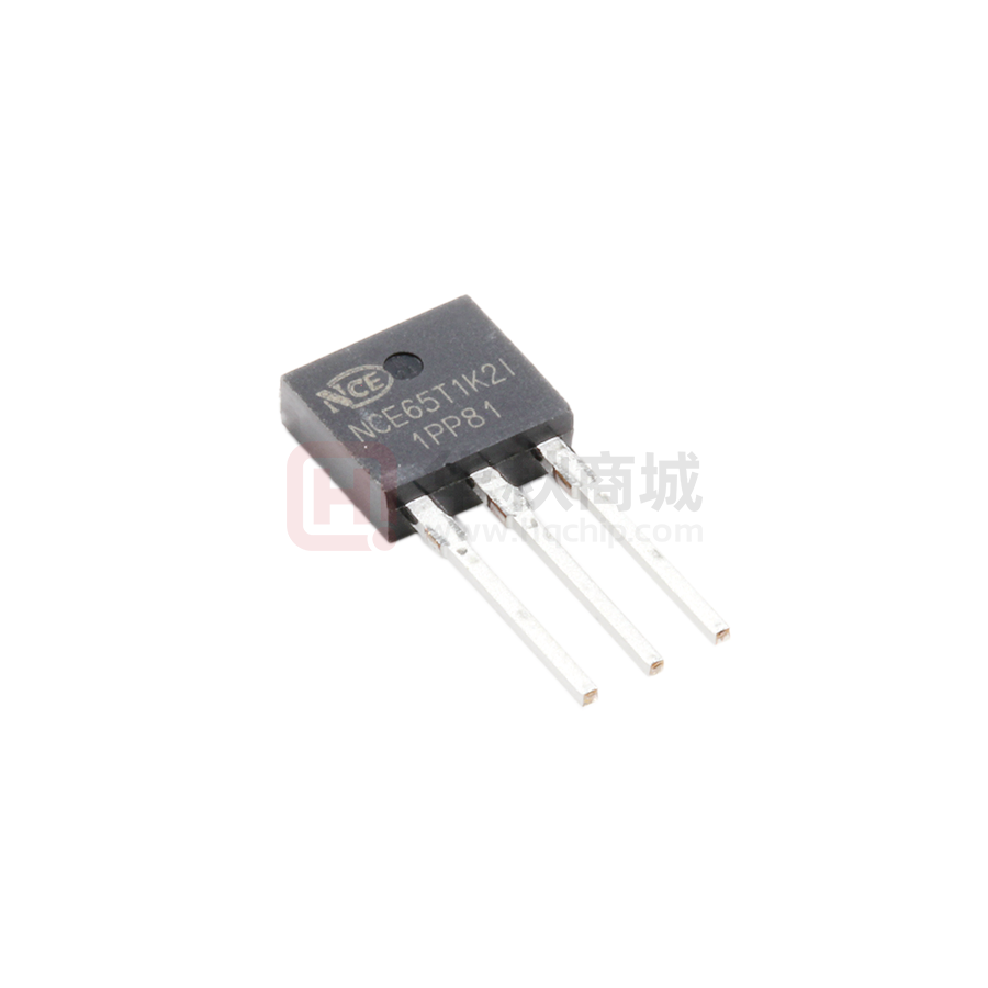
Package Marking And Ordering Information
Device
Device Package
Marking
NCE65T1K2I
TO-251
NCE65T1K2I
NCE65T1K2K
TO-252
NCE65T1K2K
TO-251
Absolute Maximum Ratings (TC=25℃)
Parameter
Symbol
Drain-Source Voltage (VGS=0V)
VDS
VGS
Gate-Source Voltage (VDS=0V) ,AC (f>1 Hz)
Continuous Drain Current at Tc=25°C
ID (DC)
Continuous Drain Current at Tc=100°C
ID (DC)
(Note 1)
IDM (pluse)
Pulsed drain current
Maximum Power Dissipation(Tc=25℃)
PD
TO-252
Table 1.
Derate above 25°C
(Note2)
Single pulse avalanche energy
(Note 1)
Avalanche current
Repetitive Avalanche energy ,tAR limited by Tjmax
(Note 1)
Wuxi NCE Power Co., Ltd
Page
1
Value
Unit
650
V
±30
V
4
A
2.5
A
16
A
41
W
0.328
W/°C
EAS
27
mJ
IAR
0.7
A
EAR
0.1
mJ
http://www.ncepower.com
V1.0
�NCE65T1K2K,NCE65T1K2I
Parameter
Symbol
Value
Unit
Drain Source voltage slope, VDS ≤480 V,
dv/dt
50
V/ns
Reverse diode dv/dt,VDS ≤480 V,ISD
很抱歉,暂时无法提供与“NCE65T1K2I”相匹配的价格&库存,您可以联系我们找货
免费人工找货- 国内价格
- 5+2.88360
- 50+2.21400
- 150+1.93320