DATA SHEET
Solid State Relay OCMOS FET
PS7801J-1A
4-PIN ULTRA SMALL FLAT-LEAD, LOW C × R (3 pF • Ω) 1-ch Optical Coupled MOS FET
−NEPOC Series−
DESCRIPTION
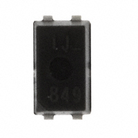
The PS7801J-1A is a low output capacitance solid state relay containing a GaAs LED on the light emitting side (input side) and MOS FETs on the output side. An ultra small flat-lead package has been provided which realizes a reduction in mounting area of about 50% compared with the PS72xx series. It is suitable for high-frequency signal control, due to its low C × R (3 pF • Ω), low output capacitance, and low offstate leakage current.
FEATURES
• Ultra small flat-lead package (4.2 (L) × 2.5 (W) × 1.85 (H) mm) • Low C × R (C × R = 2.9 pF • Ω) • Low output capacitance (Cout = 1.3 pF TYP.) • 1 channel type (1 a output) • Designed for AC/DC switching line changer • Low offset voltage • Ordering number of taping product: PS7801J-1A-F3: 3 500 pcs/reel • Pb-Free product • Safety standards • UL approved: File No. E72422
1 2 4
PIN CONNECTION
(Top View)
3 1. LED Anode 2. LED Cathode 3. MOS FET 4. MOS FET
APPLICATIONS
• Measurement equipment
The information in this document is subject to change without notice. Before using this document, please confirm that this is the latest version.
Not all products and/or types are available in every country. Please check with an NEC Electronics sales representative for availability and additional information.
Document No. PN10687EJ01V0DS (1st edition) Date Published December 2007 NS Printed in Japan
2007
�PS7801J-1A
PACKAGE DIMENSIONS (UNIT: mm)
2.5±0.3 4 3
0.2 MAX.
4.2±0.2
N
0.2±0.1
1 2 3.0 MAX.
1.85±0.05 0.15 +0.1 –0.05
4.6±0.2
3.6 +0.3 –0.4
0.4±0.1 1.27
0.2±0.1
MARKING EXAMPLE
1J
N
701
No.1 pin mark (Nicked corner)
Last number of type No. : 1J *1 *2
An initial of "NEC"
Assembly lot
7 01 (Marking details)
Week assembled Year assembled
*1 The marking corresponds to the last two digits of the part number below. PS7801J-1A *2 Bar : Pb-Free
2
Data Sheet PN10687EJ01V0DS
0.36
�PS7801J-1A
ORDERING INFORMATION
Part Number PS7801J-1A PS7801J-1A-F3 Order Number PS7801J-1A-A PS7801J-1A-F3-A Solder Plating Specification Pb-Free Packing Style 50 pcs (Tape 50 pcs cut) Embossed Tape 3 500 pcs/reel Safety Standard Approval Standard products (UL approved) Application *1 Part Number PS7801J-1A
*1 For the application of the Safety Standard, following part number should be used.
ABSOLUTE MAXIMUM RATINGS (TA = 25°C, unless otherwise specified)
Parameter Diode Forward Current (DC) Reverse Voltage Power Dissipation Peak Forward Current MOS FET Break Down Voltage Continuous Load Current Pulse Load Current
*2 *1
Symbol IF VR PD IFP VL IL ILP
Ratings 50 5.0 50 1 20 160 240
Unit mA V mW A V mA mA
(AC/DC Connection) Power Dissipation Isolation Voltage
*3
PD BV PT TA Tstg
250 500 300 −40 to +85 −40 to +100
mW Vr.m.s. mW °C °C
Total Power Dissipation Operating Ambient Temperature Storage Temperature
*1 PW = 100 μs, Duty Cycle = 1% *2 PW = 100 ms, 1 shot *3 AC voltage for 1 minute at TA = 25°C, RH = 60% between input and output Pins 1-2 shorted together, 3-4 shorted together.
RECOMMENDED OPERATING CONDITIONS (TA = 25°C)
Parameter LED Operating Current LED Off Voltage Symbol IF VF MIN. 2 0 TYP. 5 MAX. 20 0.5 Unit mA V
Data Sheet PN10687EJ01V0DS
3
�PS7801J-1A
ELECTRICAL CHARACTERISTICS (TA = 25°C)
Parameter Diode Forward Voltage Reverse Current MOS FET Off-state Leakage Current Output Capacitance Coupled LED On-state Current On-state Resistance Turn-on Time Turn-off Time
*1, 2
Symbol VF IR ILoff Cout IFon Ron ton toff RI-O CI-O IF = 5 m A VR = 5 V V D = 20 V
Conditions
MIN.
TYP. 1.1
MAX. 1.4 5.0
Unit V
μA
nA pF mA Ω ms
0.01 1.3
0.25 1.7 2.0
VD = 0 V, f = 1 MHz, t ≤ 1 s IL = 160 mA IF = 5 mA, IL = 160 mA, t ≤ 10 ms IF = 5 mA, VO = 5 V, RL = 500 Ω, PW ≥ 10 ms VI-O = 0.5 kVDC V = 0 V, f = 1 MHz 10
9
2.2 0.05 0.03
3.2 0.5 0.5
*1, 2
Isolation Resistance Isolation Capacitance
Ω 0.3 pF
*1 Test Circuit for Switching Time
IF Pulse Input VL
Input 50% 0
VO = 5 V
Input monitor Rin RL
VO monitor
Output
90%
10% ton toff
*2 The turn-on time and turn-off time are specified as input-pulse width ≥ 10 ms. Be aware that when the device operates with an input-pulse width less than 10 ms, the turn-on time and turn-off time will increase.
4
Data Sheet PN10687EJ01V0DS
�PS7801J-1A
TYPICAL CHARACTERISTICS (TA = 25°C, unless otherwise specified)
MAXIMUM FORWARD CURRENT vs. AMBIENT TEMPERATURE
100
Maximum Forward Current IF (mA) Maximum Load Current IL (mA)
MAXIMUM LOAD CURRENT vs. AMBIENT TEMPERATURE
200
80
160
60
120
40
80
20 0 –25
40
0
25
50
75
85
100
0 –25
0
25
50
75
85
100
Ambient Temperature TA (˚C)
Ambient Temperature TA (˚C)
FORWARD VOLTAGE vs. AMBIENT TEMPERATURE
1.6
Output Capacitance Cout (pF)
OUTPUT CAPACITANCE vs. APPLIED VOLTAGE
2.0 f = 1 MHz, t
很抱歉,暂时无法提供与“PS7801J-1A-F3-A”相匹配的价格&库存,您可以联系我们找货
免费人工找货