DATA SHEET DATA SHEET
PHOTOCOUPLERS
PS8601, PS8601L
HIGH SPEED ANALOG OUTPUT TYPE 8 PIN PHOTOCOUPLER
DESCRIPTION
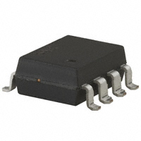
PS8601 and PS8601L is a 8-pin high speed photocoupler containing a GaAIAs LED on input side and a P-N photodiode and a high speed amplifier transistor on output side on one chip. PS8601 is in a plastic DIP (Dual In-line Package). PS8601L is lead bending type (Gull wing) for surface mount.
FEATURES
• High supply voltage • High speed response • High isolation voltage (VCC = 35 V MAX.) (tPHL, tPLH: 0.8 �s MAX.) (BV: 5 000 Vr.m.s. MIN.)
• TTL, CMOS compatible with a resistor • Taping product number (PS8601L-E3) • UL recognized [File No. E72422(s)] • VDE0884 recognized: option
APPLICATIONS
• Interface circuit for various instrumentations, control equipments. • Computer and peripheral manufactures. • Electrical isolation of TV video terminals.
ORDERING INFORMATION
PART NUMBER PS8601 PS8601L PS8601L1 PS8601L2 PS8601-V PS8601L-V PS8601L1-V PS8601L2-V 8 pin DIP 8 pin DIP, lead bending type 8 pin DIP, lead bending type (for long distance) 8 pin DIP 8 pin DIP, lead bending type 8 pin DIP, lead bending type (for long distance) VDE0884 specification products (option) • VDE Approved PACKAGE SAFETY STANDARD APPROVAL Normal specification products • UL Approved
[Handling Precaution]
This product is weak for static electricity by designed with high speed integrated circuit. So, protect against static electricity when handling.
Document No. P11650EJ2V0DS00 (2nd edition) (Previous No. LC-2362) Date Published June 1996 P Printed in Japan
©
1995
�PS8601, PS8601L
PACKAGE DIMENSIONS (Unit: mm)
DIP (Dual In-line Package)
PS8601
PIN CONNECTIONS (Top View)
8 Output 7 6 5
Lead Bending type (Gull-wing)
PS8601L
PIN CONNECTIONS (Top View)
8 Output 7 6 5
10.16 MAX. 8 5
1. 2. 3. 4.
1
2 3 Input 5. 6. 7. 8.
4
10.16 MAX. 8 5
1. 2. 3. 4.
1
2 3 Input 5. 6. 7. 8.
4 Emitter VO Base VCC
6.5
1
4 7.62
6.5
NC Anode Cathode NC
Emitter VO Base VCC
NC Anode Cathode NC
1
4
3.8 MAX.
2.8 4.55 MIN. MAX.
3.8 MAX.
0.65
1.27 MAX. 2.54 9.60 ± 0.4 0.25
M
0.05 to 0.2
0.9 ± 0.25 0.9 ± 0.25
7.62
1.34
1.27 MAX. 2.54 0.50 ± 0.10 0 to 15o 0.25
M
1.34 ± 0.10
Lead Bending type (for long distance)
PS8601L1 PS8601L2
10.16 MAX. 8 5 8
10.16 MAX. 5
6.5
6.5
11.8 ± 0.4 1 4 10.16 7.62 1 4 10.16
3.8 MAX.
2.8 4.25 MIN. MAX.
0.35
3.8 MAX.
2.54 0 to 15o 2.54 1.34 0.50 ± 0.10 0.25
M
1.27 MAX.
1.27 MAX.
0.05 to 0.2
7.62
1.34 ± 0.10
0.25
M
2
�PS8601, PS8601L
ABSOLUTE MAXIMUM RATINGS (TC = 25 �C)
Diode Forward Current Reverse Voltage Power Dissipation Detector Supply Voltage Output Voltage Output Current Power Dissipation Isolation Voltage
*1
IF VR PD VCC VO IO PC BV TA Tstg
25 5 45 35 35 8 100 5 000
mA V mW V V mA mW Vr.m.s.
Operating Temperature Storage Temperature *1
�55 to +100 �55 to +150
�C �C
AC voltage for 1 minute at TA = 25 �C, RH = 60 % between input and output.
ELECTRICAL CHARACTERISTICS (TA = 25 �C)
PARAMETER SYMBOL MIN. TYP . 1.7 MAX. UNIT TEST CONDITIONS
Diode
Forward Voltage Reverse Current Forward Voltage Temperature Coefficient Junction Capacitance
VF IR
2.2 10
V
IF = 16 mA VR = 5 V IF = 16 mA
�A
mV/�C pF
�V F �T
Ct IOH 1 IOH 2 VOL
�1.6
60 3 500 100 0.1 0.4
V = 0, f = 1 MHz IF = 0 mA, VCC = VO = 5.5 V IF = 0 mA, VCC - VO = 35 V IF = 16 mA, VCC = 4.5 V, IO = 1.2 mA IF = 16 mA, VO = Open, VCC = 35 V IF = 0 mA, VO = Open, VCC = 35 V IF = 16 mA, VCC = 4.5 V, VO = 0.4 V Vin-out = 1 kVDC V = 0, f - 1 MHz IF = 16 mA, VCC = 5 V RL = 1.9 k� IF = 16 mA, VCC = 5 V RL = 1.9 k�
Detector
High Level Output Current High Level Output Current Low Level Output Voltage
nA
�A
V
Low Level Supply Current High Level Supply Current Coupler Current Transfer Ratio
ICCL ICCH CTR 15
11
50 0.01 1
�A �A
%
Isolation Resistance Isolation Capacitance Propagation Delay Time (H � L) Propagation Delay Time (L � H)
R1-2 C1-2 tPHL *2 tPLH *2
10
�
0.7 0.5 0.8 pF
�s �s
0.3
0.8
3
�PS8601, PS8601L
*2 Test Circuit for Propagation Delay Time.
Pulse Input
IF
1 2 3 8 7 6 5
VCC = 5 V RL VO VO Monitor
IF 50 % 0 VO 1.5 V tPHL tPLH 5V 1.5 V VOL
PW = 100 µs Duty Cycle = 1/10
IF Monitor
51 Ω
4
4
�PS8601, PS8601L
TYPICAL CHARACTERISTICS (TA = 25 �C)
MAX. FORWARD CURRENT vs. AMBIENT TEMPERATURE
PC - Transistor Power Dissipation - mW 30 IF - MAX. Forward Current - mA 120 100 80 60 40 20
TRANSISTOR POWER DISSIPATION vs. AMBIENT TEMPERATURE
20
10
0
25
50
75
100
125
0
25
50
75
100
125
TA - Ambient Temperature - ˚C
TA - Ambient Temperature - ˚C
FORWARD CURRENT vs. FORWARD VOLTAGE
100 10
OUTPUT CURRENT vs. OUTPUT VOLTAGE
IF - Forward Current - mA
10 TA = 100 ˚C 50 ˚C 25 ˚C 0 ˚C –25 ˚C
IO - Output Current - mA
8 IF = 25 mA 6 IF = 20 mA IF = 15 mA 4 IF = 10 mA IF = 5 mA
1.0
0.1
2
0.01 1.0
1.2
1.4
1.6
1.8
2.0
2.2
2.4
0
0
2
4
6
8
10 12 14
16 18
20
VF - Forward Voltage - V
VO - Output Voltage - V
CURRENT TRANSFER RATIO vs. FORWARD CURRENT
50 CTR - Current Transfer Raito - % 2.0
NORMALIZED OUTPUT CURRENT vs. AMBIENT TEMPERATURE
∆CTR - Current Transfer Raito
1.8 1.6 1.4 1.2 1.0 0.8 0.6 0.4 0.2 0.0 –75 –50 Normalized to at TA = 25 ˚C VCC = 4.5 V VO = 0.4 V IF = 16 mA
40
VCC = 4.5 V VO = 0.4 V TA = 25 ˚C
30
20
10
0 .1
.5
1
5
10
50 100
–20
0
25
50
75
100 125
IF - Forward Current - mA
TA - Ambient Temperature - ˚C
5
�PS8601, PS8601L
OUTPUT VOLTAGE vs. FORWARD CURRENT
7 6
HIGH LEVEL OUTPUT CURRENT vs. AMBIENT TEMPERATURE
1000 RL
IOH - High Level Output Current - nA
VCC = 5 V IF VCC
IF = 0
VO - Output Voltage - V
5 4 3 2 1 0
10 kΩ
100
10 VCC = VO = 35 V VCC = VO = 5.5 V
RL = 1.9 kΩ 5.6 kΩ
1
0
2
4
6
8
10 12
14 16
18 20
.1 –25
0
25
50
75
100
IF - Forward Current - mA
TA - Ambient Temperature - ˚C
PROPAGATION DELAY TIME vs. LOAD RESISTANCE
tPHL, tPLH - Propagation Delay Time - µ s tPHL, tPLH - Propagation Delay Time - µ s
10 VCC = 5 V 5 IF = 16 mA tPLH 3.0 2.5 2.0 1.5 1.0 0.5
PROPAGATION DELAY TIME vs. AMBIENT TEMPERATURE
VCC = 5 V IF = 16 mA RL = 1.9 kΩ
1 .5 tPHL
tPLH
tPHL –25 0 25 50 75 100 125
.1 1 5 10 50 100 RL - Load Resistance - kΩ
0.0 –75 –50
TA - Ambient Temperature - ˚C
6
�PS8601, PS8601L
TAPING
1. TAPING DIRECTION
PS8601L-E3
2. OUTLINE AND DIMENSIONS (TAPE) Unit: mm
P0 P2 T0 D0
E
I
F
W
B
D1
P1
T1
A
3. OUTLINE AND DIMENSIONS (REEL) Unit: mm
SYMBOL A
2 ± 0.5
φ 18.0 ± 0.5
A
φ 21 ± 0.8
R1.0
4. PACKING; 1000 pieces/reel
APAN ×× 101
NEC JAPAN PS86×× N 101
SYMBOL A B D0 D1 E F P0 P1 P2 T0 T1 W
RATINGS 10.7 � 0.1 10.3 � 0.1 1.55 � 0.1 1.55 � 0.1 1.75 � 0.1 7.5 � 0.1 4.0 � 0.1 12.0 � 0.1 2.0 � 0.1 4.3 � 0.2 0.3 16 � 0.3
RATINGS 330 80 � 5.0 16.4 �0
+2.0
N
W
W
7
�PS8601, PS8601L
SOLDERING PRECAUTION
(1) Infrared reflow soldering • Peak temperature : 235 �C or lower (plastic surface) • Time : 30 s or less (Time during plastic surface temperature overs 210 �C) • No. of reflow times : Three • Flux : Rosin-base flux INFRARED RAY REFLOW TEMPERATURE PROFILE
PACKAGE’S SURFACE TEM (˚C)
(ACTUAL HEAT) to 10 s 235 ˚C MAX 210 ˚C
to 30 s 120 to 160 ˚C
60 to 90 s (PRE-HEAT)
TIME (s)
(1) Please avoid be removed the residual flux by water after the first reflow processes.
Peak Temperature 235 ˚C or lower
(2) Dip soldering • Peak temperature : 260 �C or lower • Time • Flux : 10 s or less : Rosin-base flux
8
�PS8601, PS8601L
SPECIFICATION OF VDE MARKS LICENSE DOCUMENT (VDE0884)
PARAMETER Application classification (DIN VDE0109) for rated line voltages � 300 Veff for rated line voltages � 600 Veff Climatic test class (DIN IEC 68 Teil 1/09.80) Dielectric strength maximum operating isolation voltage. Test voltage (partial discharge test procedure a for type test and random test) Upr = 1.2 � UIORM, Pd < 5 pC Test voltage (partial discharge test procedure b for random test) Upr = 1.6 � UIORM, Pd < 5 pC Highest permissible overvoltage Degree of pollution (DIN VDE 0109) Clearance distance Creepage distance Comparative tracking index (DIN IEC 112/VDE 0303 part 1) Material group (DIN VDE0109) Storage temperature range Operating temperature range Isolation resistance, minimum value UIO = 500 V dc at 25 Cel UIO = 500 V dc at Tamp maximum at least 100 Cel Safety maximum ratings (maximum permissible in case of fault, see thermal derating curve) Package temperature Current (input current IF, Psi = 0) Power (output or total power dissipation) Isolation resistance UIO = 500 V dc at 175 Cel (Tsi) Tstg Tamb CTI UIORM Upr SYMBOL SPECK UNIT
IV III 55/100/21 890 1 068 Vpeak Vpeak
Upr
1 424
Vpeak
UTR
8 000 2 > 7.0 > 7.0 175 IIIa
Vpeak
mm mm
�55 to +150 �55 to +100
10 11 10
12
Cel Cel
Ris min Ris min
ohm ohm
Tsi Isi Psi Ris min
175 400 700 10
9
Cel mA mW ohm
9
�PS8601, PS8601L
CAUTION
The Great Care must be taken in dealing with the devices in this guide. The reason is that the material of the devices is GaAs (Gallium Arsenide), which is designated as harmful substance according to the law concerned. Keep the law concerned and so on, especially in case of removal.
No part of this document may be copied or reproduced in any form or by any means without the prior written consent of NEC Corporation. NEC Corporation assumes no responsibility for any errors which may appear in this document. NEC Corporation does not assume any liability for infringement of patents, copyrights or other intellectual property rights of third parties by or arising from use of a device described herein or any other liability arising from use of such device. No license, either express, implied or otherwise, is granted under any patents, copyrights or other intellectual property rights of NEC Corporation or others. While NEC Corporation has been making continuous effort to enhance the reliability of its semiconductor devices, the possibility of defects cannot be eliminated entirely. To minimize risks of damage or injury to persons or property arising from a defect in an NEC semiconductor device, customers must incorporate sufficient safety measures in its design, such as redundancy, fire-containment, and anti-failure features. NEC devices are classified into the following three quality grades: "Standard", "Special", and "Specific". The Specific quality grade applies only to devices developed based on a customer designated "quality assurance program" for a specific application. The recommended applications of a device depend on its quality grade, as indicated below. Customers must check the quality grade of each device before using it in a particular application. Standard: Computers, office equipment, communications equipment, test and measurement equipment, audio and visual equipment, home electronic appliances, machine tools, personal electronic equipment and industrial robots Special: Transportation equipment (automobiles, trains, ships, etc.), traffic control systems, anti-disaster systems, anti-crime systems, safety equipment and medical equipment (not specifically designed for life support) Specific: Aircrafts, aerospace equipment, submersible repeaters, nuclear reactor control systems, life support systems or medical equipment for life support, etc. The quality grade of NEC devices is "Standard" unless otherwise specified in NEC's Data Sheets or Data Books. If customers intend to use NEC devices for applications other than those specified for Standard quality grade, they should contact an NEC sales representative in advance. Anti-radioactive design is not implemented in this product.
M4 96. 5
�