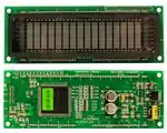
M0216MD-162MDBR2-J
Vacuum Fluorescent Display Module
RoHS Compliant
Newhaven Display International, Inc.
2661 Galvin Ct.
Elgin IL, 60124
Ph: 847-844-8795
Fax: 847-844-8796
www.newhavendisplay.com
nhtech@newhavendisplay.com
nhsales@newhavendisplay.com
�Document Revision History
Revision
Date
0
1
2
3
5/4/01
3/18/02
11/19/05
2/24/06
4
5
5/25/10
6/8/10
6
2/1/19
Description
Initial Release
Eliminate exhaust from glass design
Convert to RoHS Pb-free components
Sumida 134752B –EOL, convert to new power supply 134752C.
Current consumption increases from (170mA TYP ~230mA MAX) to
(350mA TYP ~ 400mA MAX)
User Guide Reformat
High level input current added, controller name added
Character Height Fixed
Changed by
BE
BE
SB
1. SCOPE
This specification applies to VFD module (Model No: M0216MD-162MDBR2-J).
2. FEATURES
a. Since a DC/DC converter is used, only +5Vdc power source is required to operate the module.
b. High quality display and luminance
c. ASCII and Japanese characters (CG-ROM font).
3. GENERAL DESCRIPTIONS
a. This specification becomes effective after being approved by the purchaser.
b. When any conflict is found in the specification, appropriate action should be taken upon
agreement of both parties.
c. The expected necessary service parts should be arranged by the customer before the completion
of production.
4. PRODUCT SPECIFICATIONS
4.1
Type
Table 1
Type
Digit Format
Controller
M0216MD-162MDBR2-J
5x7 Dot with Cursor
PT6314
4.2 Outer Dimensions (See Fig 7 for details)
Table 2
Parameter
Specifications
122.0 +- 1.0
44.0 +- 1.0
20.2 Max
Outer
Dimensions
Width
Height
Thickness
[2]
Unit
mm
mm
mm
�4.3 Specifications of the Display Panel
Parameter
Display Size (W*H)
Number of Digit
Character Size (W*H)
Character Pitch
Dot Size
Display Color
Specification
82.7*19
16 Digits*2 Line
3.85*9.22
3.85*8.03
0.89*0.53
Blue-Green (505 nm)
4.4 Environment Conditions
Parameter
Operating Temperature
Storage Temperature
Humidity (Operating)
Humidity (Non-operating)
Vibration (10 ~ 55 Hz)
Shock
Symbol
Topr
Tstg
Hopr
Hstg
-
Min.
-40
-50
0
0
-
4.5 Absolute Maximum Ratings
Parameter
Supply Voltage
Input Signal Voltage
Symbol
Vcc
Vis
Min.
-0.5
-0.5
4.6 Recommend Operating Conditions
Parameter
Supply Voltage
Signal (Logic) Input Voltage
Symbol
Vcc
Vis
Min.
4.5
0
4.7 DC Characteristics (Ta=+25°C, Vcc=+5.0Vdc)
Parameter
Supply Current
High Level input current
Logic Input
“H” Level
Voltage
“L” Level
Luminance
Table 3
Symbol
Icc
IIH
Vih
Vil
L
Min.
20
0.7*Vcc
100
[3]
Typ.
5.0
-
Typ.
350
200
Unit
mm
mm
mm
mm
-
Max.
+85
+95
85
90
4
40
Table 4
Unit
°C
°C
%
%
G
G
Max.
5.5
5.5
Table 5
Unit
Vdc
Vdc
Max.
5.5
Vcc
Max.
400
500
0.3*Vcc
-
Table 6
Unit
Vdc.
Vdc
Table 7
Unit
mA
µA
Vdc
Vdc
Ft-L
(cd/m2)
�[4]
�[5]
�4.8.6 SYNCHRONOUS SERIAL INTERFACE MODE
In the synchronous serial interface mode, instructions and data are sent between the host and the module using 8-bit
bytes. Two bytes are required per read/write cycle and are transmitted MSB first. The start byte contains 5 high bits, the
Read/Write (R/W) control bit, the Register Select (RS) control bit, and a low bit. The following byte contains the
instruction/data bits. The R/W bit determines whether the cycle is a read (high) or a write(low) cycle. The RS bit is used
to identify the second byte as an instruction (low) or data(high).This mode uses the Strobe (STB) control signal, Serial
Clock (SCK) input, and Serial I/O(SI/SO) line to transfer information. In a write cycle, bits are clocked into the module on
the rising edge of SCK. In a read cycle, bits in the start byte are clocked into the module on the rising edge of SCK. After
the minimum wait time, each bit in the instruction/data byte can be read from the module after each falling edge of
SCK. Each read/write cycle begin son the falling edge of STB and ends on the rising edge. To be a valid read/write cycle,
the STB must go high at the end of the cycle.
[6]
�Typical Synchronous Serial Interface Read Cycle
4.8.7 14pin Connector - Fourteen (14) of through holes are prepared for power supply and data communications.
A connector or pins may be able to soldered to the holes.
[7]
�4.8.8 Mechanical Drawing
Fig 5
1.
FUNCTION DESCRIPTIONS
1.1 Registers in VFD Controller
The VFD controller has two 8-bit registers, an instruc�on register (IR) and a data register (DR). IR stores
instruc�on codes, such as display clear and cursor shi�, and address informa�on for DD-RAM and CG-RAM. The
IR can only be wri�en from the host MPU. DR temporarily stores data to be wri�en into DD-RAM or CG-RAM
and temporarily stores data to be read from DD-RAM or CG-RAM by an internal opera�on. The DR is also used
for data storage when reading data from DD-RAM or CG-RAM. When address informa�on is wri�en into the IR,
data is read and then stored into the DR from DD-RAM or CG-RAM by internal opera�on. Data transfer between
MPU is then completed when the MPU reads the DR. A�er the read, data in DD-RAM or CG-RAM at the next
address is sent to the DFR for the next read from the MPU. By the register selector (RS) signal, these two
registers can be selected (See Table 8).
[8]
�[9]
�[10]
�[11]
�[12]
�[13]
�[14]
�[15]
�[16]
�[17]
�[18]
�[19]
�[20]
�[21]
�[22]
�[23]
�[24]
�
很抱歉,暂时无法提供与“M0216MD-162MDBR2-J”相匹配的价格&库存,您可以联系我们找货
免费人工找货