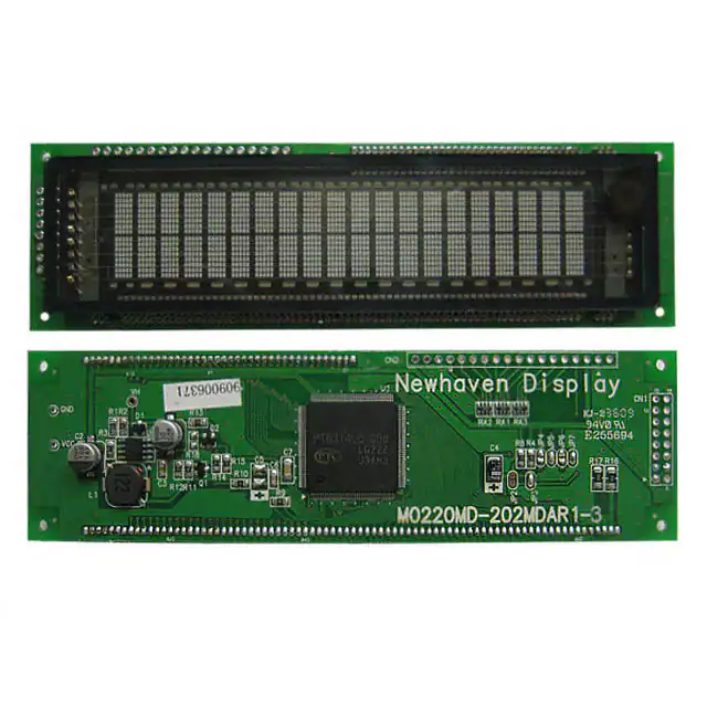
M0220MD-202MDAR1-3
Dot-matrix Character Vacuum Fluorescent Display Module
M0220MD202MDAR1-3
VFD Module
2 Lines x 20 Characters
Model
Dot-Matrix
Character Size = 3.85mm x 8.95mm
RoHS Compliant
M68 Parallel Interface
Newhaven Display International, Inc.
2661 Galvin Ct.
Elgin IL, 60124
Ph: 847-844-8795
Fax: 847-844-8796
www.newhavendisplay.com
nhtech@newhavendisplay.com
nhsales@newhavendisplay.com
�Document Revision History
Revision
0
1
2
3
4
Date
3/21/2005
9/21/2009
12/4/2009
1/26/2011
7/26/15
Description
Initial Release
Updated Driver version, modified VF glass pins
Reduce pixel size to increase brightness and lifetime
Storage temperature updated
Module redesigned
Functions and Features
2 lines x 20 characters
Built-in controller
Built-in VF AC power supply
5.0V power supply
5x8 dots with cursor
Parallel interface (serial interface selectable by onboard jumpers)
Display color: x = 0.250, y = 0.439 (Green)
[2]
Changed by
CL
CL
JT
AK
�L
A
I
Mechanical Drawing
1
2
3
4
A
Rev
D
1
Date
T
N
F
N
O
C
6
Description
E
D
I
B
C
5
B
C
D
Date
07/26/15
Unit
Gen. Tolerance
±0.3mm
2
A
3
4
mm
5
Model:
M0220MD-202MDAR1-3
6
The drawing contained herein is the exclusive property of Newhaven Display International, Inc. and shall not be copied, reproduced, and/or disclosed in any format without permission.
[3]
�Pattern Detail
[4]
�Pin Description
Parallel Interface (Default):
Pin No.
Symbol
1
2
3
4
5
6
7-10
VSS
VDD
NC (/RST)
RS
R/W
E
DB0 – DB3
11-14
DB4 – DB7
External
Connection
Power Supply
Power Supply
(MPU)
MPU
MPU
MPU
MPU
MPU
Function Description
Ground
Supply Voltage for logic (+5.0V)
No Connect (if JP2 is short, PIN3 = Active LOW reset signal)
Register Select signal RS=1: DATA RS=0: COMMAND
Read/Write select signal R/W=1: Read, R/W=0: Write
Operation Enable signal. Falling Edge Triggered
Four low order bi-directional three-state data bus lines.
These four are not used during 4-bit operation
Four high order bi-directional three-state data bus lines.
Recommended LCD connector: 2.54mm pitch pins
Serial Interface:
Pin No.
1
2
3
4
5
6
7-16
Symbol
VSS
VDD
SI/SO
STB
NC
SCK
NC
External
Connection
Power Supply
Power Supply
MPU
MPU
MPU
-
Function Description
Ground
Supply Voltage for logic (+5.0V)
Serial Data In/Out signal
Serial Strobe signal
No Connect
Serial Clock signal
No Connect
Jumper Settings
Mode
JP2
JP3
JP4
JP5
JP6
Serial
Open
Short
Open
Short
Open
Parallel i80
*1
Open
Short
Open
Open
Parallel M68 (default)
*1
Open
Short
Open
Short
*1: JP2 short enables PIN3 as external reset. JP2 open disables reset.
[5]
JP7
Short
Short
Open
�Block Diagram
[6]
�Electrical Characteristics
Item
Operating Temperature Range
Storage Temperature Range
Operating Humidity
Storage Humidity
Vibration
Shock
Supply Voltage
Supply Current (*Note 1)
Luminance
“H” Level input (*Note 2)
“L” Level input
“H” Level output
“L” Level output
Symbol
Vop
Vst
Hop
Hst
VDD
IDD
Condition
10~55Hz
Ta=25⁰C
VDD=5.0V
L
Vih
Vil
Voh
Vol
Min.
-40
-50
0
0
4.5
-
Typ.
5.0
290
Max.
+85
+95
85
90
4
40
5.5
435
Unit
⁰C
⁰C
%
%
G
G
V
mA
350
102
0.7*VDD
0.8*VDD
-
500
146
-
0.3*VDD
0.2*VDD
cd/m
ft-L
V
V
V
V
Note:
1. In-rush current can be approx. 10 times the specified supply current at power up.
2. A 10K ohm pull-up resistor is on each input signal for TTL compatibility.
Controller Information
Built-in PT6314 controller.
Please download specification at http://www.newhavendisplay.com/app_notes/PT6314.pdf
[7]
2
�Table of Commands
[8]
�Parallel Interface:
This VFD module can interface in either two 4-bit operations or one 8-bit operation. For 4-bit interface data, only four
bus lines (DB4 to DB7) are used for transfer. When to use 4-bit parallel data transfer, DB0 to DB3 keep "H" or "L". The
data transfer between the VFD module and the MPU is completed after the 4-bit data has been transferred twice. As for
the order of data transfer the four high order bits (for 8-bit operation, DB4 to DB7) are transferred before the four low
order bits (for 8-bit operation, DB0 to DB3). The busy flag (BF) are performed before transferring the higher 4 bits. BF
checks are not required before transferring the lower 4 bits.
[9]
�Serial Interface:
When data is written, it can be inputted when the STB goes to “0”. The first byte-Start Byte consists of a total 8 bits
including Synchronous bits (bit 1-bit 5), R/W (bit 6), RS (bit 7) and bit 8. The register is selected (IR or DR) by RS(bit 7)
while data write or read is selected by R/W (bit 6 =”0”). Next 8-bit instruction byte will follow closely after the defined
operation in Start Byte. Data should be keep active in rising edge of clock while it would be output in falling edge in Read
operation. Follow the protocol herein:
Serial Data Write:
Serial Data Read:
[10]
�Timing Characteristics:
M68 Write Timing:
M68 Read Timing:
[11]
�i80 Write Timing:
i80 Read Timing:
Power ON Timing:
[12]
�Serial Write Timing:
Serial Read Timing:
[13]
�Built-in Font Table
[14]
�Example Initialization Sequence
[15]
�Quality Information
Test Item
Content of Test
High Temperature storage
Endurance test applying the high
storage temperature for a long time.
Endurance test applying the low storage
temperature for a long time.
Endurance test applying the electric stress
(voltage & current) and the high thermal
stress for a long time.
Endurance test applying the electric stress
(voltage & current) and the low thermal
stress for a long time.
Endurance test applying the electric stress
(voltage & current) and the high thermal
with high humidity stress for a long time.
Endurance test applying the electric stress
(voltage & current) during a cycle of low
and high thermal stress.
Endurance test applying vibration to
simulate transportation and use.
Low Temperature storage
High Temperature
Operation
Low Temperature
Operation
High Temperature /
Humidity Operation
Thermal Shock resistance
Vibration test
Static electricity test
Test Condition
Endurance test applying electric static
discharge.
2
-30⁰C , 48hrs
1,2
+70⁰C 48hrs
2
-20⁰C , 48hrs
1,2
+40⁰C , 90% RH , 48hrs
1,2
0⁰C,30min -> +25⁰C,5min ->
+50⁰C,30min = 1 cycle
10 cycles
10-55Hz , 15mm amplitude.
60 sec in each of 3 directions
X,Y,Z
For 15 minutes
VS=800V, RS=1.5kΩ, CS=100pF
One time
Note 1: No condensation to be observed.
Note 2: Conducted after 4 hours of storage at 25⁰C, 0%RH.
Note 3: Test performed on product itself, not inside a container.
Precautions for using LCDs/LCMs
See Precautions at www.newhavendisplay.com/specs/precautions.pdf
Warranty Information and Terms & Conditions
http://www.newhavendisplay.com/index.php?main_page=terms
[16]
Note
+80⁰C , 48hrs
3
�
很抱歉,暂时无法提供与“M0220MD-202MDAR1-3”相匹配的价格&库存,您可以联系我们找货
免费人工找货