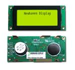
User’s Guide
NHD-10032AZ-FSY-GBW
LCM
(Liquid Crystal Display Graphic Module)
RoHS Compliant
NHD10032AZFSYGBW-
Newhaven Display
100 x 32 pixels
Version Line
Transflective
Side Yellow/Green LED B/L
STN- Gray
6:00 View
Wide Temperature (-20 ~ +70c)
For product support, contact
Newhaven Display International, LLC
2511 Technology Drive, #101
Elgin, IL 60124
Tel: (847) 844-8795 Fax: (847) 844-8796
October 18, 2007
�CONTENTS
1
2
3
4
5
6
7
8
9
10
Mechanical diagram
Block diagram
Features
Mechanical specifications
Absolute maximum ratings
Description Of Terminals
DC Electrical Characteristics
Optical Characteristics
Timing Characteristics
Display command
Newhaven Display International, LLC
Page 2 of 14
�NHD-10032AZ-FSY-GBW
1 Mechanical diagram
PIN SIGNAL
1
VSS
2
VDD
3
V0
4
RS
5
R/W
6
E1
7
E2
8
NC
100X32 Dots
STN
PERFORMANCE FEATURES
LC FLUID
TRANSFLECTIVE
REFLECTIVE
TRANSMISSIVE
TN
POLARIZER
YELLOW BLUE GRAY
HTN
COLOR
BACKLIGHT
LED
SIDE E L
6:00
12:00
VIEWING ANGLE
T E M P E R A T U R E R A N G ES T A N D A R D W I D E
PIN SIGNAL PIN SIGNAL
LED+
9
DB0
17
LED10
DB1
18
11
DB2
12
DB3
13
DB4
14
DB5
15
DB6
16
DB7
2
3
4
5
6
REVISION RECORD
Date Modify ContentsN a m e Confirm
QIU
Drawn:
Checker:
Approved:
P a g e :1-1
UNITm
: m
Model Name:
NHD-10032AZ
2002-02-21
Date:
Page 3 of 14
Newhaven Display International, LLC
�NHD-10032AZ
3
Block diagram
DB0~DB7
E1
R/W
A0
V0
VDD
VSS
COM 16
LCD
DRIVER 1
LCD PANEL
COM 16
SEG 60
LCD
E2
DRIVER 2
SEG 60
VDD
LCM
VR
Vo
VDD-Vo:LCD DRIVING VOLTAGE
4 Features
-5V
Negative
voltage
VR:10K~20K
Full dot-matrix structure with 100dots x 32 dots
1/32 duty ,1/5 bias
STN LCD, positive
Reflective LCD, yellow green
6 o’clock viewing angle
8 bits parallel data input
5 Mechanical specifications
Outline dimension : 65.0mm(L) x 28.4mm (W)
Viewing area
: 46.0mm x 18.4mm
Active area
: 42.95mm x 15.31 mm
Dot size
: 0.38mm x 0.43 mm
Dot pitch
: 0.43 mm x 0.48 mm
6 Absolute Maximum Ratings
Item
Power Voltage
Input Voltage
Operating Temperature Range
Storage Temperature Range
Newhaven Display International, LLC
Symbol
VDD -VSS
VO
VOP
TST
Min
0
VSS
-20
-30
Max
7.0
VDD
+70
+80
Unit
V
Page 4 of 14
�NHD-10032AZ
7 Description Of Terminals
Pin
No.
1
2
3
Input/
Output
Pin Name
VSS
VDD
VO
External
Connection
Power
Supply
4
RS
Input
5
R/W
Input
MPU
6
7
8
E1
E2
NC
Input
Input
MPU
MPU
DB0-DB3
Input/output
MPU
DB4-DB7
Input/output
MPU
9
/
12
13
/
16
MPU
Function
Signal ground for LCM
VDD: +5V
VLCD adjustment
Register select input
“0”:Instruction register (when writing)
Busy flag address counter (When reading)
“1”: Data register (when writing & reading)
Read/write select signal
“0” for writing, “1” for reading
Chip enable active “L”, SEG (1~60)
Chip enable active “L”, SEG (61~120)
Not connected
Low-order lines of data bus with 3-state,
Bi-directional function for use in data
Transaction with the MPU. These lines are
Not used when interfacing with a 4-bit
Microprocessor.
High-order lines of data bus with 3-state,
bi-directional function for use in data
Transactions with the MPU. DB7 may also
be used to check the busy flag.
8 DC Electrical Characteristics
Parameter
Supply voltage for LCD
Input voltage
Supply current
Input leakage current
“H” l evel input voltage
Symbol
VDD VO
VDD
IDD
ILKG
VIH
“L” level input voltage
VIL
“H” level output voltage
“L” level output voltage
VOH
VOL
Newhaven Display International, LLC
Conditions
TA =25
VDD=5.0V;TA =25
Twice initial value
or less
LOH=0.25mA
LOL=1.6mA
Min.
2.2
5.5
1.5
1.0
VDD
Unit
V
V
mA
A
V
0
0.6
V
0.4
V
V
3
Type
4.5
0.75
Max.
2.4
Page 5 of 14
�NHD-10032AZ
9 Optical Characteristics
For TN Type Display Module (Ta=25 , VDD=5.0V 0.25V)
Item
Symbol Condition Min.
Typ.
Cr 4
Viewing angle
-25
-30
Contrast ratio
Cr
2
Response time(rise)
Tr
120
Response time(fall)
Tr
120
Max.
Unit
deg
30
For STN Type Display Module (Ta=25 , VDD=5.0V 0.25V)
Item
Symbol Condition Min.
Typ.
Cr 2
Viewing angle
-60
-40
Contrast ratio
Cr
6
Response time(rise)
Tr
150
Response time(fall)
Tr
150
150
150
ms
ms
Max.
35
40
Unit
deg
250
250
ms
ms
10 Timing Characteristics
MPU bus read/write 1(80-family MPU)
A0. /CS
t aw8
R/W
t cyc8
t cc
t ds8
t ah8
t dh8
DB0~DB7
WRITE
t acc8
t acc8
DB0~DB7
READ
Newhaven Display International, LLC
Page 6 of 14
�NHD-10032AZ
Item
System cycle time
Address setup time
Address hold time
Data setup time
Data hold time
Control pulse width
RD access time
Output disable time
symbol
t cyc8
t aw8
t ah8
t ds8
t dh8
t cc
t cc8
t ch8
Conditions
Min.
1000
20
10
80
10
200
Max.
CL=100pf
90
60
10
unit
ns
ns
ns
ns
ns
ns
ns
ns
MPU bus read/write 2(68-family MPU)
t cyc6
E
t aw6
t ew
t ds6
R/W
t ah6
A0. /CS
t dh6
DB0~DB7
WRITE
DB0~DB7
READ
Item
System cycle time
Address setup time
Address hold time
Data setup time
Data hold time
Access time
Output disable time
Enable
pulse Read
width
Write
Newhaven Display International, LLC
t oh6
t acc6
symbol
t cyc6
t aw6
t ah6
t ds6
t dh6
t acc6
t oh6
t ew
Conditions
CL=100pf
Min.
1000
20
10
80
10
10
100
80
Max.
90
60
unit
ns
ns
ns
ns
ns
ns
ns
ns
ns
Page 7 of 14
�NHD-10032AZ
11 Display command
Parameter
A0
E
R/W
D7
D6
D5
D4
D3
D2
D1
D0
Display
ON /OFF
0
1
0
1
0
1
0
1
1
1
0/1
Display
start line
0
1
0
1
1
0
Set
page
address
0
1
0
1
0
1
Set column
(segment)
address
0
1
0
Read
status
0
Write
display
data
1
0
1
1
0
Bu
sy
Display start address
(0 to 31)
1
1
0
Page (0
to 3)
A
D
C
ON/
OFF
0
Turns display on or off
1: ON ; 0 : OFF
Specifies RAM line corresponding
to top line of display
Sets display RAM page in page
address register
Sets display RAM
address in column
register
Column address (0 to 79)
R
E
S
E
T
Note
column
address
Reads the following status:
0
0
0
0
BUSY 1: Busy
0: Ready
ADC
0: CCW output
1: CW output
ON/OFF 1: Display off
0: Display on
RESET 1: Being reset
0: Normal
Write data
Write data from data bus into
display RAM
Read data
Read data from display RAM onto
data bus
Read
display
data
1
0
1
Select ADC
0
1
0
1
0
1
0
0
0
0
0/1
0
1
0
1
0
1
0
0
1
0
0/1
0
1
0
1
0
1
0
1
0
0
0/1
Read-modify
write
0
1
0
1
1
1
0
0
0
0
0
Read-modify-write ON
End
Reset
0
0
1
1
0
0
1
1
1
1
1
1
0
0
1
0
1
0
1
1
0
0
Read-modify-write OFF
Software reset
Static
driver
ON/OFF
Select duty
0: CW output 1: CCW output
Selects static driving operation.
1: static driver, 0: Normal driving
Select LCD duty cycle
1: 1/32, 0: 1/16
Table 3 is the command table. The SED1520 series identifies a data bus using a combination of
A0 and R/W (RD or WR signals. As the MPU translates a command in the internal timing only
(independent from the external clock). Its speed is very high. The bus y check is usually not
required.
Display ON/OFF (AEH, AFH)
A0
0
E (RD) R/W (/WR)
1
0
Newhaven Display International, LLC
D7
1
D6
0
D5
1
D4
0
D3
1
D2
1
D1
1
D0
D
Page 8 of 14
�NHD-10032AZ
The command turns the display on and off
D=1: display ON
D=0: display OFF
Display start line (C0H~DFH)
This command specifies the line address shown if Figure 3 and indicates the display line that
corresponds to COM0. the display area begins at the specified line address and continues the
line address increment direction. This area having the number of lines of the specified display
duty is displayed. If the line address is changed dynamically by this command the vertical
smooth scrolling and paging can be used.
A0
E (RD) R/W (/WR)
D7
D6
D5
0
1
0
1
1
0
This command loads the display start line register.
D4
A4
A4
0
0
A3
0
0
A2
0
0
A1
0
0
A0
0
1
Line address
0
1
/
/
/
/
/
/
1
1
1
1
1
1F
D3
A3
D2
A2
D1
A1
D0
A0
Set page address (B8H~BBH)
This command specifies the page address that corresponds to the low address of the display
data RAM when it is accessed by the MPU. Any bit of the display data RAM can be accessed
when its page address and column address are specified. The display status is not changed
even when the page address is changed.
A0
0
E (RD) R/W (/WR)
1
0
D7
1
D6
0
D5
1
D4
1
D3
1
D2
0
D1
A1
D0
A0
This command loads the page address register.
A1
0
0
1
1
Newhaven Display International, LLC
A0
0
1
0
1
Page
0
1
2
3
Page 9 of 14
�NHD-10032AZ
Set column address (00H~4FH)
This command specifies a column address of the display data RAM. When the display data RAM
is accessed by the MPU continuously, the column address is incremented by 1 each time it is
accessed from the set address. Therefore, the MPU can access to data continuously. The
column address stops to be incremented at address 80, and the page address is not changed
continuously.
A0
0
E (RD) R/W (/WR)
1
0
D7
0
D6
A6
D5
A5
D4
A4
D3
A3
D2
A2
D1
A1
D0
A0
This command loads the column address register.
A6
0
0
A5 A4
0
0
0
0
A3
0
0
A2 A1
0
0
0
0
A0
0
1
Column address
0
1
/
/
/
/
/
/
/
/
1
0
0
1
1
1
1
4F
Read status
A0
0
E (RD) R/W (/WR)
1
0
D7
D6
Busy ADC
D5
On/off
D4
Reset
D3
A3
D2
A2
D1
A1
D0
A0
Reading the command I/O register (A0=0) yields system status information.
The busy bit indicates whether the driver will accept a command or not.
Busy=1: the driver is currently executing a command or is resetting. No new command will be
accepted.
Busy=0: the driver will accept a new command.
The ADC bit indicates the way column addresses are assigned to segment drivers.
ADC=1 Normal. Column address n segment driver n.
ADC=0 Inverted. Column address 79 u segment driver u.
The ON/OFF bit indicates the current status of the display.
It is the inverse of the polarity of the display ON/OFF command.
ON/OFF=1: display off
ON/OFF=0: display on
The RESET bit indicates whether the driver is executing a hardware or software reset or if it is
in normal operating mode.
Reset=1: currently executing reset command.
Reset=0: normal operation
Newhaven Display International, LLC
Page 10 of 14
�NHD-10032AZ
Write display data
A0
1
E (RD) R/W (/WR)
1
0
D7
D6
D5
D4
D3
Write data
D2
D1
D0
Writes 8-bit of data into the display data RAM, at a location specified by the contents of the
column address and page address registers and then increments the column address register by
one.
Read display data
A0
1
E (RD) R/W (/WR)
0
1
D7
D6
D5
D4
D3
Read data
D2
D1
D0
Reads 8-bit of data from the data I/O latch, updates the contents of the I/O latch with display
data from the display data RAM location specified by the contents of the column address and
page address registers and then increments the column address register.
After loading a new address into the column address register one dummy read is required before
valid data is obtained.
Select ADC (A0H, A1H)
A0
0
E (RD) R/W (/WR)
1
0
D7
1
D6
0
D5
1
D4
0
D3
0
D2
0
D1
0
D0
D
This command selects the relationship between display data RAM column addresses and
segment drivers.
D=1: SEG0 column address 4FH,…(inverted).
D=0: SEG0 column address 00H,…(normal).
This command is provided to reduce restrictions on the placement of driver ICs and routing of
traces during printed circuit board design. See Figure 2 go a table of segments and column
addresses for the two values of D.
Static drive ON/OFF (A4H, A5H)
A0
E (RD) R/W (/WR)
D7
D6
D5
D4
0
1
0
1
0
1
0
Forces display on and all common outputs to be selected.
D=1:static drive on
D=0:static drive off
Newhaven Display International, LLC
D3
0
D2
1
D1
0
D0
D
Page 11 of 14
�NHD-10032AZ
Select duty (A8H; A9H)
A0
E (RD) R/W (/WR)
D7
D6
D5
D4
D3
D2
D1
D0
0
1
0
1
0
1
0
1
0
0
D
This command sets the duty cycle of the LCD drive and is only valid for the SED1520F and
SED1522F.it is invalid for the SED1521F, which performs passive operation. The duty cycle of
the SED1521F is determined by the externally generated FR signal.
SED1520
SED1522
D=: 1/32 duty cycle 1/16 duty cycle
D=: 1/16 duty cycle 1/8 duty cycle
When using the SED1520F0A, SED1522F0A (having a built-in oscillator) and the SED1521F0A
continuously, set the duty as follows:
SED1521FOA
1/32
1/16
1/32
1/16
1/32
1/16
1/116
SED1522FOA
1/8
SED1520FOA
READ-MODIFY-WRITE (E0H)
A0
0
E (RD) R/W (/WR)
1
0
D7
1
D6
1
D5
1
D4
0
D3
0
D2
0
D1
0
D0
0
This command defeats column address register auto -increment after data reads. The current
contents of the column address register are saved. This mode remains active until an end
command is repeated.
Operation sequence during cursor display
When the end command is entered, the column address is returned to the one used during input
of read-modify-write command. This function can reduce the load of MPU when data change is
repeated at a specific
Display area (such as cursor blinking).
*Any command other than data read or write can be used in the read-modify-write mode.
However, the column address set command cannot be used.
Newhaven Display International, LLC
Page 12 of 14
�NHD-10032AZ
set page address
set column address
read-modify-write
dummy read
read data
write data
completed?
end
END (EEH)
A0
0
E (RD) R/W (/WR)
1
0
D7
1
D6
1
D5
1
D4
0
D3
1
D2
1
D1
1
D0
0
This command cancels read-modify-write mode and restores the contents of the column address
register to their value prior to the receipt of the read-modify-write command.
Return
column address
N
N+1
read-modify-write mode is selected
Newhaven Display International, LLC
N+m
N
End
End
Page 13 of 14
�NHD-10032AZ
RESET (E2H)
A0
0
E (RD) R/W (/WR)
1
0
D7
1
D6
1
D5
1
D4
0
D3
1
D2
1
D1
1
D0
0
This command clears
The display start line register.
And set page address register to 3 page.
It does not affect the contents of the display data RAM.
When the power supply is turned on, a Reset signal is entered in the RES pin. The Reset
command cannot be used instead of this Reset signal.
Newhaven Display International, LLC
Page 14 of 14
�


 工商网监
湘ICP备2023018690号
工商网监
湘ICP备2023018690号
