Product Specification
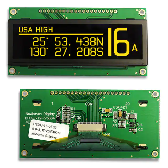
NHD-3.12-25664UCY2
Newhaven Display International, Inc.
2661 Galvin Court, Elgin, IL 60124 USA
Ph: 847.844.8795 | Fx: 847.844.8796
www.newhavendisplay.com
REACH
Compliant
RoHS
Compliant
�Table of Contents
Document Revision History .......................................................................................................................... 2
Mechanical Drawing .................................................................................................................................... 3
Pin Description ............................................................................................................................................ 4
Wiring Diagrams .......................................................................................................................................... 5
On-Board Jumper Options ........................................................................................................................... 6
Electrical Characteristics .............................................................................................................................. 7
MPU Interface ............................................................................................................................................. 8
Example Initialization Sequence................................................................................................................... 9
Quality Information ................................................................................................................................... 10
Additional Resources
➢ Support Forum: https://support.newhavendisplay.com/hc/en-us/community/topics
➢ GitHub: https://github.com/newhavendisplay
➢ Example Code: https://support.newhavendisplay.com/hc/en-us/categories/4409527834135-Example-Code/
➢
Knowledge Center: https://www.newhavendisplay.com/knowledge_center.html
➢ Quality Center: https://www.newhavendisplay.com/quality_center.html
➢ Precautions for using LCDs/LCMs: https://www.newhavendisplay.com/specs/precautions.pdf
➢ Warranty / Terms & Conditions: https://www.newhavendisplay.com/terms.html
1
�Document Revision History
Revision
Date
Description
Changed By
0
05/01/2011
Initial Product Release
-
1
02/22/2013
Electrical characteristics and mechanical drawing updated
JN
2
05/02/2016
Supply Current Updated
SB
3
04/02/2020
Mechanical Characteristics Updated
SB
4
08/04/2020
Reformatted 2D Mechanical Drawings
AS
5
07/15/2022
PCB Redesign offering multiple driving methods. Updated Electrical
characteristics, Mechanical Drawing.
JT
2
�1
A
2
Mechanical Drawing
3
4
5
6
7
SYMBOL
8
REVISION
DATE
A
B
B
C
C
Pin Assignment
0.3
0.28
D
Segment 112
Segment 367
( Column 1 )
( Column 256 )
Common A0
( Column 128 )
( Row 64 )
Segment 240
( Column 129 )
0.28
0.3
Segment 239
Common B0
( Row 64 )
Common A63
Common B63
( Row 1 )
Detail "A"
( Row 1 )
2
3
2
3
4
5
6
7-14
VDD
NC or BC_VDD
D/C
R/W or /WR
E or /RD
DB0 – DB7
D
NC or VCC
/RES
17
/CS
18
19
20
NC or G_VDD
BS1
BS0
E
Standard Tolerance:
Product Descrip�on: 3.12” Yellow Graphic OLED
1. OLED Driver IC: SSD1322
2. OLED Interface: 8-bit 6800/8080 Parallel, 3-/4-wire Serial
3. OLED Power Requirement: 3.3V/310mA
4. Ma�ng Connector: 20 pin, 2.54mm pitch
1
Symbol
VSS
15
16
E
F
Pin No.
1
(Unless otherwise specified)
Linear:
±0.3mm
Unless otherwise specified:
• Dimensions are in Millimeters
• Third Angle Projection
Revision:
Drawing/Part Number:
NHD-3.12-25664UCY2
Drawn By:
Drawn Date:
J.Thomas
07/15/2022
Approved By:
Approved Date:
Do Not Scale Drawing
Size:
J.Thomas
07/15/2022
-
A3
Scale:
NS
Sheet 1 of 1
This drawing is solely the property of Newhaven Display International, Inc.
The information it contains is not to be disclosed, reproduced or copied in
whole or part without written approval from Newhaven Display.
4
5
6
7
8
F
�Pin Description
Parallel Interface:
Pin No.
1
2
3
Symbol
VSS
VDD
NC or BC_VDD
External Connection
Power Supply
Power Supply
-
4
5
D/C
R/W or /WR
MPU
MPU
6
E or /RD
MPU
7-14
15
DB0 – DB7
NC or VCC
MPU
-
16
17
18
/RES
/CS
NC or G_VDD
MPU
MPU
-
19
20
BS1
BS0
MPU
MPU
Function Description
Ground
Supply Voltage for OLED and logic.
Default: No Connect
Supply Voltage for Boost Converter: See Jumper Option #1
Register select signal. D/C=0: Command, D/C=1: Data
6800-interface:
Read/Write select signal, R/W=1: Read, R/W=0: Write
8080-interface:
Active LOW Write signal.
6800-interface:
Operation enable signal. Falling edge triggered.
8080-interface:
Active LOW Read signal.
8-bit Bi-directional data bus lines.
Default: No Connect
Supply Voltage for OLED Panel: See Jumper Option #2
Active LOW Reset signal.
Active LOW Chip Select signal.
Default: No Connect
Supply Voltage for Internal Regulator: See Jumper Option #3
MPU Interface Select signal.
MPU Interface Select signal.
Serial Interface:
Pin No.
1
2
3
Symbol
VSS
VDD
NC or BC_VDD
External Connection
Power Supply
Power Supply
-
4
D/C
MPU
5-6
7
8
9
10-14
15
VSS
SCLK
SDIN
NC
VSS
NC or VCC
Power Supply
MPU
MPU
Power Supply
-
16
17
18
/RES
/CS
NC or G_VDD
MPU
MPU
-
19
20
BS1
BS0
MPU
MPU
Function Description
Ground
Supply Voltage for OLED and logic.
Default: No Connect
Supply Voltage for Boost Converter: See Jumper Option #1
Register select signal. D/C=0: Command, D/C=1: Data
Tie LOW for 3-wire Serial Interface.
Ground
Serial Clock signal.
Serial Data Input signal.
No Connect
Ground
Default: No Connect
Supply Voltage for OLED Panel: See Jumper Option #2
Active LOW Reset signal.
Active LOW Chip Select signal.
Default: No Connect
Supply Voltage for Internal Regulator: See Jumper Option #3
MPU Interface Select signal.
MPU Interface Select signal.
4
�MPU Interface Pin Selections
Pin
Name
6800 Parallel
8-bit interface
8080 Parallel
8-bit interface
1
1
1
0
BS1
BS0
3-wire
Serial
Interface
0
1
4-wire
Serial
Interface
0
0
MPU Interface Pin Assignment Summary
Bus
Interface
8-bit 6800
8-bit 8080
3-wire SPI
4-wire SPI
D7
Data/Command Interface
D6 D5 D4 D3
D2
D1
D[7:0]
D[7:0]
Tie LOW
NC
SDIN
Tie LOW
NC
SDIN
D0
SCLK
SCLK
Control Signals
E
R/W /CS
D/C
E
R/W /CS
D/C
/RD /WR /CS
D/C
Tie LOW
/CS Tie LOW
Tie LOW
/CS
D/C
/RES
/RES
/RES
/RES
/RES
Wiring Diagrams
5
�On-Board Jumper Options
Default Jumper Setting
R14
R15
R18
R1
Close
Open
Open
Open
Description
(default) OLED Logic Circuit + Boost converter + OLED panel are powered from VDD
(pin #2). This allows the full module to be powered by a single low-voltage supply.
Jumper Option #1 - Independent Supply Voltage for Boost Converter (BC_VDD)
R14
R15
R18
R1
Description
Open
Close
Open
Open
Boost converter + OLED panel are powered from BC_VDD (pin #3). OLED Logic Circuit
is powered from VDD (pin #2). This allows for increased efficiency through the boost
converter, by allowing a supply voltage up to +12V at its input, BC_VDD (pin #3).
Jumper Option #2 – External Supply Voltage for OLED Panel (VCC)
R14
R15
R18
R1
Open
Open
Close
Open
Description
OLED panel is powered from VCC (pin #15) – boost converter is not used.
OLED Logic Circuit is powered from VDD (pin #2). This allows for maximum module
efficiency, and drastically reduced total current consumption.
Jumper Option #3 – External Supply Voltage for Internal Regulator (G_VDD)
R14
R15
R18
R1
Description
See Description
Close
OLED Internal Regulator + Logic Circuit are powered from G_VDD (pin #18) – boost
converter is powered from VDD (pin #2). Disabling the internal regulator reduces
power consumption. Booster circuit must be driven by alternative method.
Default Jumper Setting
Jumper Option #1 (BC_VDD)
Jumper Option #2 (VCC)
Jumper Option #3 (G_VDD)
For detailed electrical information on each jumper option, please see the Electrical Characteristics table below.
6
�Electrical Characteristics
Item
Operating Temperature Range
Storage Temperature Range
Supply Voltage for Module
Supply Current for Module
Symbol
Top
Tst
VDD
IDD
Supply Voltage for Module
Supply Current for Module
Supply Voltage for Boost Converter
VDD
IDD
BC_VDD
Supply Current for Boost Converter
BC_IDD
Supply Voltage for Module
Supply Current for Module
Supply Voltage for OLED Panel
Supply Current for OLED Panel
Supply Voltage for Logic
Supply Current for Module
VDD
IDD
VCC
ICC
G_VDD
G_IDD
Condition
Absolute Max
Absolute Max
Default Jumper Setting
VDD=3.3V, 100% ON
Jumper Option #1
VDD=3.3V
BC_VDD=5.0V, 100% ON
BC_VDD=12.0V, 100% ON
Jumper Option #2
VDD=3.3V
VCC=12V, 100% ON
Jumper Option #3
VDD=3.3V
Min.
-40
-40
Typ.
-
Max.
+85
+90
Unit
⁰C
⁰C
2.8
-
3.3
310
3.5
340
V
mA
2.8
2.8
-
3.3
170
150
55
3.5
200
12
170
70
V
µA
V
mA
mA
2.8
11.5
-
3.3
170
12
45
3.5
200
12.5
55
V
µA
V
mA
2.4
-
2.5
100
2.6
120
V
µA
Sleep Mode Current
IDDSLEEP
25
120
µA
“H” Level input
Vih
0.8*VDD
VDD
V
“L” Level input
Vil
VSS
0.2*VDD
V
“H” Level output
Voh
0.9*VDD
VDD
V
“L” Level output
Vol
VSS
0.1*VDD
V
Note: The electrical characteristics shown above for Jumper Option #1 and Jumper Option #2 apply only when the on-board
jumpers are configured accordingly. By default, only Default Jumper Setting supply voltage and current (in bold) need to be
considered. For details, see On-Board Jumper Options section on previous page.
Optical Characteristics
Item
Top
Bottom
Left
Right
Symbol
Condition
Min.
Typ.
Max.
Unit
ϕY+
80
⁰
Optimal
ϕY80
⁰
Viewing
θX80
⁰
Angles
θX+
80
⁰
Contrast Ratio
CR
2000:1
Rise
TR
10
us
Response Time
Fall
TF
10
us
Brightness
LV
TOP = 25°C
60
80
cd/m2
50% Checkerboard
Lifetime
40,000
60,000
Hrs.
Note: Lifetime at typical temperature is based on accelerated high-temperature operation. Lifetime is tested at
average 50% pixels on and is rated as Hours until Half-Brightness. The Display OFF command can be used to extend
the lifetime of the display. Luminance of active pixels will degrade faster than inactive pixels. Residual (burn-in)
images may occur. To avoid this, every pixel should be illuminated uniformly.
7
�Controller Information
Built in SSD1322 Controller
For detailed information please download datasheet:
https://support.newhavendisplay.com/hc/en-us/articles/4414477846679-SSD1322
MPU Interface
6800-MPU Parallel Interface
The parallel interface consists of 8 bi-directional data pins, R/W, D/C, E, and /CS.
A LOW on R/W indicates write operation, and HIGH on R/W indicates read operation.
A LOW on D/C indicates “Command” read or write, and HIGH on D/C indicates “Data” read or write.
The E input serves as data latch signal, while /CS is LOW. Data is latched at the falling edge of E signal.
Function
Write Command
Read Status
Write Data
Read Data
E
↓
↓
↓
↓
R/W
0
1
0
1
/CS
0
0
0
0
D/C
0
0
1
1
8080-MPU Parallel Interface
The parallel interface consists of 8 bi-directional data pins, /RD, /WR, D/C, and /CS.
A LOW on D/C indicates “Command” read or write, and HIGH on D/C indicates “Data” read or write.
A rising edge of /RS input serves as a data read latch signal while /CS is LOW.
A rising edge of /WR input serves as a data/command write latch signal while /CS is LOW.
Function
Write Command
Read Status
Write Data
Read Data
/RD
1
↑
1
↑
/WR
↑
1
↑
1
/CS
0
0
0
0
D/C
0
0
1
1
Alternatively, /RD and /WR can be kept stable while /CS serves as the data/command latch signal.
Function
Write Command
Read Status
Write Data
Read Data
/RD
1
0
1
0
/WR
0
1
0
1
/CS
↑
↑
↑
↑
D/C
0
0
1
1
Serial Interface (4-wire)
The 4-wire serial interface consists of serial clock SCLK, serial data SDIN, D/C, and /CS.
D0 acts as SCLK and D1 acts as SDIN. D2 should be left open. D3~D7, E, and R/W should be connected to GND.
Function
Write Command
Write Data
/RD
Tie LOW
Tie LOW
/WR
Tie LOW
Tie LOW
/CS
0
0
D/C
0
1
D0
↑
↑
SDIN is shifted into an 8-bit shift register on every rising edge of SCLK in the order of D7, D6,…D0.
D/C is sampled on every eighth clock and the data byte in the shift register is written to the GDRAM or
command register in the same clock. Note: Read is not available in serial mode
8
�Serial Interface (3-wire)
The 3-wire serial interface consists of serial clock SCLK, serial data SDIN, and /CS.
D0 acts as SCLK and D1 acts as SDIN. D2 should be left open. D3~D7, E, R/W, and D/C should be connected to
GND.
Function
Write Command
Write Data
/RD
Tie LOW
Tie LOW
/WR
Tie LOW
Tie LOW
/CS
0
0
D/C
Tie LOW
Tie LOW
D0
↑
↑
SDIN is shifted into an 9-bit shift register on every rising edge of SCLK in the order of D/C, D7, D6,…D0.
D/C (first bit of the sequential data) will determine if the following data byte is written to the Display Data
RAM (D/C = 1) or the command register (D/C = 0). Note: Read is not available in serial mode
Example Initialization Sequence
Set_Command_Lock(0x12);
Set_Display_On_Off(0x00);
Set_Column_Address(0x1C,0x5B);
Set_Row_Address(0x00,0x3F);
Set_Display_Clock(0x91);
Set_Multiplex_Ratio(0x3F);
Set_Display_Offset(0x00);
Set_Start_Line(0x00);
Set_Remap_Format(0x14);
// Unlock Basic Commands (0x12/0x16)
// Display Off (0x00/0x01)
// Set Clock as 80 Frames/Sec
// 1/64 Duty (0x0F~0x3F)
// Shift Mapping RAM Counter (0x00~0x3F)
// Set Mapping RAM Display Start Line (0x00~0x7F)
// Set Horizontal Address Increment
// Column Address 0 Mapped to SEG0
// Disable Nibble Remap
// Scan from COM[N-1] to COM0
// Disable COM Split Odd Even
// Enable Dual COM Line Mode
Set_GPIO(0x00);
// Disable GPIO Pins Input
Set_Function_Selection(0x01);
// Enable Internal VDD Regulator
Set_Display_Enhancement_A(0xA0,0xFD);
// Enable External VSL
Set_Contrast_Current(0x9F);
// Set Segment Output Current
Set_Master_Current(0x0F);
// Set Scale Factor of Segment Output Current Control
//Set_Gray_Scale_Table();
// Set Pulse Width for Gray Scale Table
Set_Linear_Gray_Scale_Table();
//set default linear gray scale table
Set_Phase_Length(0xE2);
// Set Phase 1 as 5 Clocks & Phase 2 as 14 Clocks
Set_Display_Enhancement_B(0x20);
// Enhance Driving Scheme Capability (0x00/0x20)
Set_Precharge_Voltage(0x1F);
// Set Pre-Charge Voltage Level as 0.60*VCC
Set_Precharge_Period(0x08);
// Set Second Pre-Charge Period as 8 Clocks
Set_VCOMH(0x07);
// Set Common Pins Deselect Voltage Level as 0.86*VCC
Set_Display_Mode(0x02);
// Normal Display Mode (0x00/0x01/0x02/0x03)
Set_Partial_Display(0x01,0x00,0x00); // Disable Partial Display
Set_Display_On_Off(0x01);
9
�Quality Information
Test Item
Content of Test
High Temperature storage
Test the endurance of the display at high
storage temperature.
Test the endurance of the display at low
storage temperature.
Test the endurance of the display by
applying electric stress (voltage & current)
at high temperature.
Test the endurance of the display by
applying electric stress (voltage & current)
at low temperature.
Test the endurance of the display by
applying electric stress (voltage & current)
at high temperature with high humidity.
Test the endurance of the display by
applying electric stress (voltage & current)
during a cycle of low and high
temperatures.
Test the endurance of the display by
applying vibration to simulate
transportation and use.
Low Temperature storage
High Temperature
Operation
Low Temperature
Operation
High Temperature /
Humidity Operation
Thermal Shock resistance
Vibration test
Atmospheric Pressure test
Static electricity test
Test the endurance of the display by
applying atmospheric pressure to simulate
transportation by air.
Test the endurance of the display by
applying electric static discharge.
Test Condition
Note
+90⁰C, 240hrs
2
-40⁰C, 240hrs
1,2
+85⁰C, 240hrs
2
-40⁰C, 240hrs
1,2
+60⁰C, 90% RH, 240hrs
1,2
-40⁰C,30min -> 25⁰C,5min ->
85⁰C,30min = 1 cycle
100 cycles
10-22Hz, 1.5mm amplitude.
22-500Hz, 1.5G
30min in each of 3 directions
X, Y, Z
115mbar, 40hrs
3
3
VS=800V, RS=1.5kΩ, CS=100pF
One time
Note 1: No condensation to be observed.
Note 2: Conducted after 2 hours of storage at 25⁰C, 0%RH.
Note 3: Test performed on product itself, not inside a container.
Evaluation Criteria:
1: Display is fully functional during operational tests and after all tests, at room temperature.
2: No observable defects.
3: Luminance >50% of initial value.
4: Current consumption within 50% of initial value
10
�