NHD-4.3-480272EF-ASXN#-CTP 数据手册
NHD-4.3-480272EF-ASXN#-CTP
TFT (Thin-Film-Transistor) Color Liquid Crystal Display Module
NHD4.3480272EFASXN#CTP-
Newhaven Display
4.3” Diagonal
480xRGBx272 Pixels
Model
Built-in Driver / No Controller
Sunlight Readable
TFT
TN, Wide Temperature
RoHS Compliant
Capacitive Touch Panel with Controller
Newhaven Display International, Inc.
2661 Galvin Ct.
Elgin IL, 60124
Ph: 847-844-8795
Fax: 847-844-8796
www.newhavendisplay.com
nhtech@newhavendisplay.com
nhsales@newhavendisplay.com
�Document Revision History
Revision
0
1
2
3
4
5
6
7
8
Date
10/6/15
1/10/17
3/11/17
10/25/17
7/23/18
10/4/18
5/2/19
6/25/19
3/22/21
9
3/30/21
Description
Initial Release
Mechanical Drawing, Electrical & Optical Char. Updated
Driver IC Updated
CTP Cable Location Fixed
Display Thickness Updated to Show CTP Adhesive
CTP Driver & Panel Updated
CTP Timing Note Added
FPC Layout Updated
Updated Silkscreen on FPC, Chromaticity Values & Quality
Information
Updated 2D Mechanical Drawing for Tape Size
Functions and Features
•
•
•
•
•
480xRGBx272 resolution, up to 16.7M colors
16-LED backlight
24-Bit RGB interface
Sunlight Readable
Capacitive touch panel with controller
o 10-point multi-touch input
o Gesture input
▪ Zoom In/Out
▪ Swipe Up/Down/Left/Right
[2]
Changed by
SB
SB
SB
SB
SB
SB
SB
SB
AS
AS
�1
A
2
3
4
5
Mechanical Drawing
8
DATE
Overall: 4.65±0.3
TFT: 2.95±0.2
CTP: 1.4±0.1
95.44±0.15 (VA)
5.03
95.04(LCD A.A)
4.00
7
REVISION
A
105.50±0.1
(4.18)
6
SYMBOL
.30
4-R0
(52.75)
Adhesive (0.3)
TFT 4.3"
480(RGB) X 272
53.86(LCD A.A)
67.20±0.1
B
54.20±0.15
(31.11)
R GB
B
VIEW DIRECTION
Pin Assignment
White silk on FPC
NHD-4.3-480272EF_B
*18.75±0.5
5±0.5
Stiffener
4040
1
Contact side
YD
XR
1
20.35±0.3
A
D
25.22±0.5
A
A2
A1
K2
K1
*45.67±0.5
K
C
PI Stiffer
0.3±0.05
20.5±0.2
45.6±0.5
40
3.5±0.3
1.4
0.35
1.4
1
E
F
Notes:
1. Display Size:
2. Op�mal View:
3. Display Mode:
4. Driver IC:
5. Supply Voltage:
6. Backlight:
7. Luminance:
8. Touch Panel:
1
4.3” TFT
6:00
Transmissive / Normally White / An�-Glare
ST7282T2
3.3V
White LED / 25.6V / 40 mA (Typ)
830 cd/m² (Typ)
PCAP
2
3
Pin No.
1
2
3
4
5
6
0.3
P0.5*39=19.5±0.1
DETAIL A
C
D
E
(UNLESS OTHERWISE SPECIFIED)
A1
K1
A2
K2
5
Symbol
LEDK
LEDA
GND
VDD
[R0-R7]
[G0-G7]
[B0-B7]
GND
CLK
DISP
HSYNC
VSYNC
DEN
NC
GND
NC
NC
NC
NC
STANDARD TOLERANCE:
B/L CIRCUIT DIAGRAM
4
Symbol
VDD
GND
SCL
SDA
/INT
/RESET
Pin No.
1
2
3
4
5-12
13-20
21-28
29
30
31
32
33
34
35
36
37
38
39
40
6
LINEAR: ±0.3mm
REVISION:
DRAWING/PART NUMBER:
NHD-4.3-480272EF-ASXN#-CTP
UNLESS OTHERWISE SPECIFIED:
DRAWN BY:
- DIMENSIONS ARE IN MILLIMETERS
DRAWN DATE:
- THIRD ANGLE PROJECTION
A. Shah
3/30/2021
APPROVED BY:
A3
A. Shah
SCALE:
APPROVED DATE:
DO NOT SCALE DRAWING
1B
SIZE:
NS
3/30/2021
SHEET 1 OF 1
THIS DRAWING IS SOLELY THE PROPERTY OF NEWHAVEN DISPLAY INTERNATIONAL, INC.
THE INFORMATION IT CONTAINS IS NOT TO BE DISCLOSED, REPRODUCED OR COPIED IN
WHOLE OR PART WITHOUT WRITTEN APPROVAL FROM NEWHAVEN DISPLAY.
7
8
F
�Pin Description
TFT:
Pin No.
1
2
3
4
5-12
13-20
21-28
29
30
31
32
33
34
35
36
37
38
39
40
Symbol
LEDLED+
GND
VDD
[R0-R7]
[G0-G7]
[B0-B7]
GND
CLK
DISP
HSYNC
VSYNC
DE
NC
GND
NC
NC
NC
NC
External Connection
Power Supply
Power Supply
Power Supply
Power Supply
MPU
MPU
MPU
Power Supply
MPU
MPU
MPU
MPU
MPU
Power Supply
-
Function Description
Backlight Cathode (Ground)
Backlight Anode (40mA @ 25.6V)
Ground
Supply Voltage for LCD and logic (3.3V)
Red Data signals
Green Data signals
Blue Data signals
Ground
Data sample Clock signal
Display ON/OFF signal
Line synchronization signal
Frame synchronization signal
Data Enable signal
No Connect
Ground
No Connect
No Connect
No Connect
No Connect
Recommended LCD connector: 0.5mm pitch 40-Conductor FFC. Molex p/n: 54104-4033
Backlight connector: on LCD connector
Mates with: ---
Capacitive Touch Panel:
Pin No.
1
2
3
4
5
Symbol
VDD
GND
SCL
SDA
/INT
External Connection
Power Supply
Power Supply
MPU
MPU
MPU
6
/RESET
MPU
Function Description
Power supply for logic (3.3V)
Ground
Serial I2C Clock (Requires pull-up resistor)
Serial I2C Data (Requires pull-up resistor)
Interrupt signal from T.P. module to host (Requires pull-up
resistor)
Active LOW Reset signal (Do not tie to VDD)
Recommended connector: 1.0mm pitch 6-Conductor FFC. Molex p/n: 52271-0679
[4]
�Electrical Characteristics
TFT:
Item
Operating Temperature Range
Storage Temperature Range
Supply Voltage
Supply Current
“H” level input
“L” level input
“H” level output
“L” level output
Backlight Supply Current
Backlight Supply Voltage
Backlight Lifetime*
Symbol
TOP
TST
VDD
IDD
VIH
VIL
VOH
VOL
Condition
Absolute Max
Absolute Max
VDD = 3.3V
-
Min.
-20
-30
3.0
12
0.8 * VDD
GND
0.9 * VDD
GND
Typ.
3.3
25
-
Max.
+70
+80
3.6
50
VDD
0.3 * VDD
VDD
0.1 * VDD
Unit
⁰C
⁰C
V
mA
V
V
V
V
ILED
VLED
-
ILED = 40 mA
ILED = 40mA
TOP = 25°C
22.4
20,000
40
25.6
50,000
50
27.2
-
mA
V
Hrs.
*Backlight lifetime is rated as Hours until half-brightness, under normal operating conditions. The LED of the backlight is driven by current drain; drive voltage is for
reference only. Drive voltage must be selected to ensure backlight current drain is below MAX level stated.
Capacitive Touch Panel:
Item
Operating Temperature Range
Storage Temperature Range
Supply Voltage
Supply Current (Operating)
Supply Current (Hibernate)
“H” level input
“L” level input
“H” level output
“L” level output
Symbol
TOP
TST
VDD
IDD
IDD
VIH
VIL
VOH
VOL
Condition
Absolute Max
Absolute Max
VDD = 3.3V
TOP = 25°C
-
Min.
-20
-30
3.0
12
0.7 * VDD
GND
0.7 * VDD
GND
Typ.
3.3
13
1.0
-
Max.
+70
+80
3.6
14.5
VDD
0.3 * VDD
VDD
0.3 * VDD
Unit
⁰C
⁰C
V
mA
µA
V
V
V
V
Symbol
ϕY+
ϕYθXθX+
CR
LV
TR + TF
XR
YR
XG
YG
XB
YG
XW
YW
Condition
Min.
400
660
0.523
0.297
0.260
0.563
0.093
0.047
0.223
0.271
Typ.
55
75
75
75
500
830
25
0.573
0.347
0.310
0.613
0.143
0.097
0.273
0.321
Max.
30
0.623
0.397
0.360
0.663
0.193
0.147
0.323
0.371
Unit
⁰
⁰
⁰
⁰
cd/m2
ms
-
Optical Characteristics
Optimal
Viewing
Angles
Item
Top
Bottom
Left
Right
Contrast Ratio
Luminance
Response Time
Rise + Fall
Red
Green
Chromaticity
Blue
White
Cr ≥ 10
ILED = 40 mA
TOP = 25°C
-
[5]
�Capacitive Touch Panel Material Characteristics
Property
IC
ITO Glass Thickness
Surface Hardness
Transparency
Operating Humidity
Storage Humidity
Requirement
FT5426
0.55
≥6
82%
20~90
20~90
Unit
mm
H
RH
RH
Driver/Controller Information
TFT:
Built-in Sitronix ST7282T2 Driver.
Please download specification at http://www.newhavendisplay.com/appnotes/datasheets/LCDs/ST7282T2.pdf
Capacitive Touch Panel:
Built-in FocalTech FT5426 controller.
Please download specification at http://www.newhavendisplay.com/appnotes/datasheets/touchpanel/FT5x26.pdf
[6]
�Capacitive Touch Panel Registers
Register No.
Access
Register Name
Bits
01h
RO
Gesture ID
[7:0]
02h
RO
Touch Points
[7:0]
03h
RO
TOUCH1_Event_Flag
[7:6]
03h
04h
05h
06h
07h
08h
RO
RO
RO
RO
RO
RO
TOUCH1_XH
TOUCH1_XL
TOUCH1_YH
TOUCH1_YL
TOUCH1_Weight
TOUCH1_Misc
[3:0]
[7:0]
[3:0]
[7:0]
[7:0]
[3:0]
09h
RO
TOUCH2_Event_Flag
[7:6]
09h
0Ah
0Bh
0Ch
0Dh
0Eh
RO
RO
RO
RO
RO
RO
TOUCH1_XH
TOUCH2_XL
TOUCH2_YH
TOUCH2_YL
TOUCH2_Weight
TOUCH2_Misc
[3:0]
[7:0]
[3:0]
[7:0]
[7:0]
[3:0]
0Fh
RO
TOUCH3_Event_Flag
[7:6]
0Fh
10
11h
12h
13h
14h
RO
RO
RO
RO
RO
RO
TOUCH3_XH
TOUCH3_XL
TOUCH3_YH
TOUCH3_YL
TOUCH3_Weight
TOUCH3_Misc
[3:0]
[7:0]
[3:0]
[7:0]
[7:0]
[3:0]
15h
RO
TOUCH4_Event_Flag
[7:6]
15h
16h
17h
18h
1Ah
RO
RO
RO
RO
RO
TOUCH4_XH
TOUCH4_XL
TOUCH4_YH
TOUCH4_YL
TOUCH4_Misc
[3:0]
[7:0]
[3:0]
[7:0]
[3:0]
1Bh
RO
TOUCH5_Event_Flag
[7:6]
Value
10
18h
1Ch
14h
48h
49h
00
0-Ah
0
1
2
3
0 -1
00 - FFh
0 -1
00 - FFh
00-0Fh
0
1
2
3
0 -1
00 - FFh
0 -1
00 - FFh
00-0Fh
0
1
2
3
0 -1
00 - FFh
0 -1
00 - FFh
00-0Fh
0
1
2
3
0 -1
00 - FFh
0 -1
00 - FFh
00-0Fh
0
1
2
3
[7]
Description
Swipe Up
Swipe Down
Swipe Left
Swipe Right
Zoom Out
Zoom In
No gesture
0: No touch detected
A: 10 touch points detected
Put Down
Put Up
Contact
Reserved
Upper 4 bits of X touch coordinate
Lower 8 bits of X touch coordinate
Upper 4 bits of Y touch coordinate
Lower 8 bits of Y touch coordinate
Touch Weight
Touch Area
Put Down
Put Up
Contact
Reserved
Upper 4 bits of X touch coordinate
Lower 8 bits of X touch coordinate
Upper 4 bits of Y touch coordinate
Lower 8 bits of Y touch coordinate
Touch Weight
Touch Area
Put Down
Put Up
Contact
Reserved
Upper 4 bits of X touch coordinate
Lower 8 bits of X touch coordinate
Upper 4 bits of Y touch coordinate
Lower 8 bits of Y touch coordinate
Touch Weight
Touch Area
Put Down
Put Up
Contact
Reserved
Upper 4 bits of X touch coordinate
Lower 8 bits of X touch coordinate
Upper 4 bits of Y touch coordinate
Lower 8 bits of Y touch coordinate
Touch Area
Put Down
Put Up
Contact
Reserved
�Register No.
1Bh
1Ch
1Dh
1Eh
1Fh
20
Access
RO
RO
RO
RO
RO
RO
Register Name
TOUCH5_XH
TOUCH5_XL
TOUCH5_YH
TOUCH5_YL
TOUCH5_Weight
TOUCH5_Misc
Bits
[3:0]
[7:0]
[3:0]
[7:0]
[7:0]
[3:0]
21h
RO
TOUCH6_Event_Flag
[7:6]
21h
22h
23h
24h
25h
26h
RO
RO
RO
RO
RO
RO
TOUCH6_XH
TOUCH6_XL
TOUCH6_YH
TOUCH6_YL
TOUCH6_Weight
TOUCH6_Misc
[3:0]
[7:0]
[3:0]
[7:0]
[7:0]
[3:0]
27h
RO
TOUCH7_Event_Flag
[7:6]
27h
28h
29h
2Ah
2Bh
2Ch
RO
RO
RO
RO
RO
RO
TOUCH7_XH
TOUCH7_XL
TOUCH7_YH
TOUCH7_YL
TOUCH7_Weight
TOUCH7_Misc
[3:0]
[7:0]
[3:0]
[7:0]
[7:0]
[3:0]
2Dh
RO
TOUCH8_Event_Flag
[7:6]
2Dh
2Eh
2Fh
30
31h
32h
RO
RO
RO
RO
RO
RO
TOUCH8_XH
TOUCH8_XL
TOUCH8_YH
TOUCH8_YL
TOUCH8_Weight
TOUCH8_Misc
[3:0]
[7:0]
[3:0]
[7:0]
[7:0]
[3:0]
33h
RO
TOUCH9_Event_Flag
[7:6]
33h
34h
35h
36h
37h
38h
RO
RO
RO
RO
RO
RO
TOUCH9_XH
TOUCH9_XL
TOUCH9_YH
TOUCH9_YL
TOUCH9_Weight
TOUCH9_Misc
[3:0]
[7:0]
[3:0]
[7:0]
[7:0]
[3:0]
39h
RO
TOUCH10_Event_Flag
[7:6]
39h
3Ah
3Bh
3Ch
RO
RO
RO
RO
TOUCH10_XH
TOUCH10_XL
TOUCH10_YH
TOUCH10_YL
[3:0]
[7:0]
[3:0]
[7:0]
Value
0 -1
00 - FFh
0 -1
00 - FFh
00-0Fh
0
1
2
3
0 -1
00 - FFh
0 -1
00 - FFh
00-0Fh
0
1
2
3
0 -1
00 - FFh
0–1
00 - FFh
00-0Fh
0
1
2
3
0–1
00 - FFh
0–1
00 - FFh
00-0Fh
0
1
2
3
0-1
00 - FFh
0–1
00 - FFh
00 - 0Fh
0
1
2
3
0–1
00 - FFh
0–1
00 - FFh
[8]
Description
Upper 4 bits of X touch coordinate
Lower 8 bits of X touch coordinate
Upper 4 bits of Y touch coordinate
Lower 8 bits of Y touch coordinate
Touch Weight
Touch Area
Put Down
Put Up
Contact
Reserved
Upper 4 bits of X touch coordinate
Lower 8 bits of X touch coordinate
Upper 4 bits of Y touch coordinate
Lower 8 bits of Y touch coordinate
Touch Weight
Touch Area
Put Down
Put Up
Contact
Reserved
Upper 4 bits of X touch coordinate
Lower 8 bits of X touch coordinate
Upper 4 bits of Y touch coordinate
Lower 8 bits of Y touch coordinate
Touch Weight
Touch Area
Put Down
Put Up
Contact
Reserved
Upper 4 bits of X touch coordinate
Lower 8 bits of X touch coordinate
Upper 4 bits of Y touch coordinate
Lower 8 bits of Y touch coordinate
Touch Weight
Touch Area
Put Down
Put Up
Contact
Reserved
Upper 4 bits of X touch coordinate
Lower 8 bits of X touch coordinate
Upper 4 bits of Y touch coordinate
Lower 8 bits of Y touch coordinate
Touch Weight
Touch Area
Put Down
Put Up
Contact
Reserved
Upper 4 bits of X touch coordinate
Lower 8 bits of X touch coordinate
Upper 4 bits of Y touch coordinate
Lower 8 bits of Y touch coordinate
�Register No.
3Dh
3Eh
Access
RO
RO
Register Name
TOUCH10_Weight
TOUCH10_Misc
Bits
[7:0]
[3:0]
Value
00-FFh
00-0Fh
80h
RW
ID_G_MC_THGROUP
[7:0]
00-FFh
81h
RW
ID_G_MC_THPEAK
[7:0]
00-FFh
85h
RW
ID_G_THDIFF
[7:0]
00-FFh
86h
RW
ID_G_CTRL
[1:0]
0-1
88h
89h
RW
RW
ID_G_PERIODACTIVE
ID_G_PERIODMONITOR
[3:0]
[7:0]
3h-Eh
1Eh-FFh
A1h
RO
ID_G_LIB_VERSION_H
[7:0]
00-FFh
A2h
RO
ID_G_LIB_VERSION_L
[7:0]
00-FFh
A3h
RO
ID_G_CHIPER_HIGH
[7:0]
00-FFh
A4h
RW
ID_G_MODE
[0]
A5h
RW
ID_G_PMODE
[1:0]
A6h
RO
ID_G_FIRMID
[7:0]
00-FFh
A8h
RO
ID_G_VENODRID
[7:0]
00-FFh
C0h
RW
ID_G_GLOVE_MODE_EN
[0]
C1h
RW
ID_G_COVER_MODE_EN
[0]
0
1
0
1
3
0
1
0
1
[9]
Description
Touch Weight
Touch Area
Mutual-Capacitive touch Threshold / 4
Default: 4Bh
Mutual-Capacitive Peak Threshold / 4
Default: 46h
Points Filtering Range Threshold / 16
Default: A0
Allowed to switch to monitor mode or not
(1: Allowed, 0: Not Allowed)
Period of Active Status
Timer to enter “idle” while in Monitor (ms)
App library version high-byte
Default: 0
App library version low-byte
Default: 2h
Chip Vendor ID
Default: 54h
INT Trigger Mode
INT Polling Mode
Active
Monitor
Sleep
Firmware ID Number
Default: 2
CTPM Vendor’s Chip ID
Default: 79h
Glove Mode Switch Disable
Glove Mode Switch Enable
Cover Mode Switch Disable
Cover Mode Switch Enable
�Timing Characteristics – TFT Display
Parallel RGB input timing requirement
Item
DCLK Frequency
DCLK Period
HSYNC
VSYNC
Period Time
Display Period
Back Porch
Front Porch
Pulse Width
Period Time
Display Period
Back Porch
Front Porch
Pulse Width
Symbol
FCLK
TCLK
Th
Thdisp
Thbp
Thfp
Thw
Tv
Tvdisp
Tvbp
Tvfp
Tvw
Min.
9
10
485
3
2
1
275
2
1
1
[10]
Typ.
12
50
525
480
43
2
1
285
272
12
1
1
Max.
15
532
50
2
1
303
30
1
1
Unit
MHz
µS
DCLK
DCLK
DCLK
DCLK
DCLK
H
H
H
H
H
Remark
R=10KΩ, 1µF
By H_Blanking Setting
By V_Blanking Setting
�-
SYNC Mode Timing
[11]
�-
SYNC-DE Mode Timing
[12]
�Input setup timing requirement
Item
System Operation Timing
VDD Power Source Slew Time
GRB Pulse Width
Input / Output Timing
CLK pulse Duty
Hsync Width
Hsync Period
Vsync setup time
Vsync hold time
Hsync setup time
Hsync hold time
Data setup time
Data hold time
SD output stable time
Symbol
Min.
Typ.
Max.
Unit
TPOR
tRSTW
10
50
20
-
ms
µS
TCW
Thw
Th
Tvst
Tvhd
Thst
Thhd
Tdsu
Tdhd
Tst
40
1
50
12
12
12
12
12
12
-
50
60
-
60
65
12
%
DCLK
µS
ns
ns
ns
ns
ns
ns
µS
GD output rise and fall time
Tgst
-
-
6
µS
- Clock And Data Input Timing Diagram
[13]
Conditions
From 0V to 99% VDD
R=10KΩ, 1µF
Output settled within +20mV
Loading = 6.8k+28.2pF
Output settled (5%~95%)
Loading = 4.7k+29.8pF
�Power On/Off Sequence
-
Power On Sequence
[14]
�-
Power Off Sequence
[15]
�Timing Characteristics – Capacitive Touch Panel
Data Transfer Format
Parameter
SCL Frequency
Bus free time between a STOP & START condition
Hold time Repeated START condition
Data Setup Time
Setup time for a repeated START condition
Setup time for a STOP condition
Min
0
1.3
0.6
100
0.6
0.6
[16]
Max
400
-
Unit
KHz
µs
µs
ns
µs
µs
�Power ON/Reset Sequence
Power On Time
Power Cycle Requirement
Power ON Sequence
Reset sequence
Parameter
Tris
Tpdt
Trtp
Tpon
Tvdr*
Trsi
Trst*
Description
Rise time from 0.1VDD to 0.9VDD
Time of the voltage of supply being below 0.3V
Time of resetting to be low before powering on
Time to start reporting after power on
Reset time after applying VDD
Time to start reporting after reset
Reset Time
Min
5
100
1
1
*Note: If Reset is tied to VDD data corruption can occur
[17]
Max
5
200
200
-
Unit
ms
ms
µs
ms
ms
ms
ms
�Sample code to read touch data:
i2c_start();
i2c_tx(0x70);
i2c_tx(0x00);
i2c_stop();
//Slave Address (Write)
//Start reading address
i2c_start();
i2c_tx(0x71);
//Slave Address (Read)
for(i=0x00;i 25⁰C,5min >70⁰C,60min = 1 cycle
20 cycles
10-50Hz, 5G Acceleration
30 Min. Each Direction
X, Y, Z
Air: ±8kV 150pF/330Ω, 5 Times
Contact: ±4kV 150pF/330Ω, 5
Times
Note 1: No condensation to be observed.
Note 2: Conducted after 4 hours of storage at 25⁰C, 0%RH.
Note 3: Test performed on product itself, not inside a container.
Precautions for using LCDs/LCMs
See Precautions at www.newhavendisplay.com/specs/precautions.pdf
Warranty Information
See Terms & Conditions at http://www.newhavendisplay.com/index.php?main_page=terms
[19]
Note
+80⁰C , 96 Hrs.
3
�
NHD-4.3-480272EF-ASXN#-CTP 价格&库存
很抱歉,暂时无法提供与“NHD-4.3-480272EF-ASXN#-CTP”相匹配的价格&库存,您可以联系我们找货
免费人工找货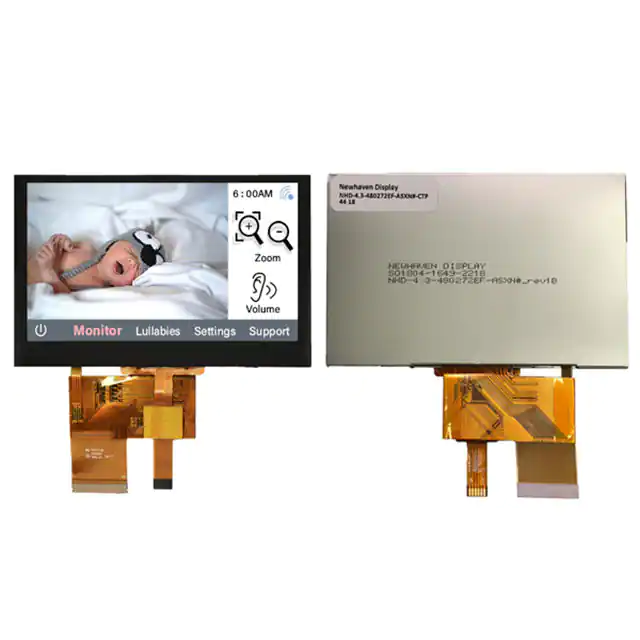


 工商网监
湘ICP备2023018690号
工商网监
湘ICP备2023018690号