NHD-5.0-800480TF-ATXL#-CTP 数据手册
Product Specification
NHD-5.0-800480TF-ATXL#-CTP
Newhaven Display International, Inc.
2661 Galvin Court, Elgin, IL 60124 USA
Ph: 847.844.8795 | Fx: 847.844.8796
www.newhavendisplay.com
REACH
Compliant
RoHS
Compliant
�Table of Contents
Document Revision History .......................................................................................................................... 2
Mechanical Drawing .................................................................................................................................... 3
Pin Description ............................................................................................................................................ 4
Driver/Controller Information ..................................................................................................................... 5
Electrical Characteristics .............................................................................................................................. 6
Optical Characteristics ................................................................................................................................. 6
Capacitive Touch Panel Registers ................................................................................................................. 7
Capacitive Touch Panel Material Characteristics........................................................................................... 9
Timing Characteristics – TFT Display ........................................................................................................... 10
Timing Characteristics – Capacitive Touch Panel ......................................................................................... 14
Quality Information ................................................................................................................................... 17
Additional Resources
➢ Support Forum: https://support.newhavendisplay.com/hc/en-us/community/topics
➢ GitHub: https://github.com/newhavendisplay
➢ Example Code: https://support.newhavendisplay.com/hc/en-us/categories/4409527834135-Example-Code/
➢
Knowledge Center: https://www.newhavendisplay.com/knowledge_center.html
➢ Quality Center: https://www.newhavendisplay.com/quality_center.html
➢ Precautions for using LCDs/LCMs: https://www.newhavendisplay.com/specs/precautions.pdf
➢ Warranty / Terms & Conditions: https://www.newhavendisplay.com/terms.html
1
�Document Revision History
Revision
Date
Description
Changed By
0
03/20/2013
Initial Release
AK
1
08/28/2013
Electrical Characteristics updated
AK
2
09/16/2014
Electrical Characteristics updated
ML
3
04/01/2015
CTP mechanical dimensions updated
AK
4
09/02/2015
Driver, Electrical, Optical characteristics updated
AK
5
10/27/2015
Backlight lifetime rating added
AK
6
10/30/2015
Datasheet Reformat
SB
7
01/18/2016
CTP Controller Updated, Updated Brightness Rating
SB
6
02/23/2016
Corrected Notes on Drawing, Updated CTP Supply Voltage
SB
7
04/05/2016
Updated Brightness Rating
SB
8
07/07/2016
Mechanical Drawing Updated
SB
9
07/22/2016
Electrical Characteristics
TM
10
04/14/2017
Supply Current Updated
SB
11
07/27/2017
CTP Registers updated
SB
12
07/13/2018
Drawing Updated to Show Accurate Thickness
SB
13
08/14/2018
CTP Bonding Tape Thickness Increased to 0.3mm
SB
14
09/21/2018
Updated CTP Driver & Panel
SB
15
10/10/2018
TFT Driver IC Updated
SB
16
05/02/2019
CTP Timing Note Added
SB
17
07/10/2019
Timing Information Updated
SB
18
01/14/2020
Driver Change to ILI6122, Optical Characteristics Updated
SB
19
04/22/2020
Added Information for DE Mode Operation
TM
20
05/06/2020
Production Line Changed:
AS
Part Revision Updated from Rev1C to Rev1D
21
03/22/2021
Updated Silkscreen on FPC
AS
22
05/11/2021
Updated Mechanical Drawing
JT
23
10/26/2021
Updated CTP IC
ZP
24
11/19/2021
Removed RW Registers from Register List
CJ
Updated CTP Register A6h Default Value to 7.
25
08/04/2022
Updated CTP IC to FT5326DQ8-003, TFT Luminance Updated, CTP
Transmittance Updated, Updated Mechanical Drawing
CJ
2
�1
A
2
Mechanical Drawing
3
4
5
6
SYMBOL
7
8
REVISION
DATE
A
Newhaven Display
NHD-5.0-800480TF-ATXL#-CTP
Date Code
TFT Pinout
Part Label (type/format may vary)
B
B
C
C
D
D
CTP Pinout
E
F
Product Descrip�on: 5” Premium TFT w/ Capaci�ve Touch
1. TFT Driver IC: ILI6122, CTP IC: FT5426DQ8-003
2. TFT Interface: 24-Bit RGB, CTP Interface: I2C
3. TFT Power Requirement: 3.3V, Backlight: 60mA (19.2V Reference)
4. Op�cal Features: Normally White, Transmissive, 527 cd/m2
5. TFT Ma�ng Connector: 40pin, 0.5mm pitch; Ex. Molex 54104-4031
6. CTP Ma�ng Connector: 6pin, 1.0mm pitch; Ex. Molex 52271-0679
7. EMI Shielding
1
2
3
4
E
Standard Tolerance:
(Unless otherwise specified)
Linear:
±0.3mm
Unless otherwise specified:
A+
5
• Dimensions are in Millimeters
• Third Angle Projection
K6
Drawing/Part Number:
NHD-5.0-800480TF-ATXL#-CTP
Drawn By:
Drawn Date:
C. Johnson
08/04/2022
Approved By:
Approved Date:
Do Not Scale Drawing
C. Johnson
08/04/2022
Revision:
Size:
-
A3
Scale:
NS
Sheet 1 of 1
This drawing is solely the property of Newhaven Display International, Inc.
The information it contains is not to be disclosed, reproduced or copied in
whole or part without written approval from Newhaven Display.
7
8
F
�Pin Description
TFT:
Pin No.
1
2
3
4
5-12
13-20
21-28
29
30
31
32
33
34
35
36
37
38
39
40
Symbol
LEDLED+
GND
VDD
[R0-R7]
[G0-G7]
[B0-B7]
GND
CLKIN
STBYB
HSD
VSD
DEN
NC
GND
XR
YD
XL
YU
External Connection
LED Power Supply
LED Power Supply
Power Supply
Power Supply
MPU
MPU
MPU
Power Supply
MPU
MPU
MPU
MPU
MPU
Power Supply
-
Function Description
Ground for Backlight
Backlight Power Supply (60mA @ ~19.2V)
Ground
Power supply for LCD and logic (3.3V)
Red Data Signals
Green Data Signals
Blue Data Signals
Ground
Clock for input data (Rising Edge)
1: Normal Operation;0: Standby Mode
Line synchronization signal
Frame synchronization signal
Data Enable signal; Positive Polarity (Required in DE mode)
No Connect
Ground
No Connect
No Connect
No Connect
No Connect
Recommended LCD Connector: 0.5mm pitch 40-Conductor FFC. Molex P/N: 54104-4031 (top contact)
Backlight Connector: on LCD connector
Mates with: ---
The ILI6122 driver IC is configured for DE Mode by default which eliminates the need to depend on HSD and
VSD timing signals. Using DE mode in place of Sync mode, the display will no longer be affected by changes to
the sync timing or porch settings in the event of a driver IC change. This will maintain a consistent display
performance for any driver IC changes that may occur in the future.
The ILI6122 driver will treat the data on the Dx[7:0] RGB data bus as active display data while DEN is at “H”
level and ignore the data on the Dx[7:0] RGB data bus while DEN is at “L” level.
Sync Mode can still be provided as the default setting but will need to be ordered as a custom option.
Capacitive Touch Panel:
Pin No.
1
2
3
4
5
6
Symbol
VCC
GND
SCL
SDA
/INT
/RESET
External Connection
Power Supply
Power Supply
MPU
MPU
MPU
MPU
Function Description
Power supply for logic (3.3V)
Ground
Serial I2C Clock (Requires pull-up resistor)
Serial I2C Data (Requires pull-up resistor)
Interrupt signal from touch panel module to host
Active LOW Reset signal (Do not tie to VCC)
Recommended Connector: 1.0mm pitch 6-Conductor FFC. Molex P/N: 52271-0679
4
�Driver/Controller Information
TFT:
Built-in ILI6122 Source Driver: https://support.newhavendisplay.com/hc/en-us/articles/4414554619671-ILI6122
Built-in ILI5960D Gate Driver: https://support.newhavendisplay.com/hc/en-us/articles/4414531730583--ILI5960D
Capacitive Touch Panel:
Built-in FocalTech FT5426DQ8-003 controller.
Please download specification at https://support.newhavendisplay.com/hc/en-us/articles/4414392845079-FT5x26
5
�Electrical Characteristics
TFT:
Item
Operating Temperature Range
Storage Temperature Range
Supply Voltage
Supply Current
“H” Level input
“L” Level input
“H” Level output
“L” Level output
Backlight Supply Current
Backlight Supply Voltage
Backlight Lifetime*
Symbol
TOP
TST
VDD
IDD
VIH
VIL
VOH
VOL
Condition
Absolute Max
Absolute Max
VDD = 3.3V
-
Min.
-20
-30
3.0
39
0.7 * VDD
GND
VDD - 0.4
GND
Typ.
3.3
78
-
Max.
+70
+80
3.6
117
VDD
0.3 * VDD
VDD
0.4
Unit
⁰C
⁰C
V
mA
V
V
V
V
ILED
VLED
-
ILED = 60mA
TOP = 25°C
16.8
-
60
19.2
30,000
75
20.4
-
mA
V
Hrs.
-
*Backlight lifetime is rated as Hours until half-brightness, under normal operating conditions. The LED of the backlight is driven by current drain; drive voltage is for
reference only. Drive voltage must be selected to ensure backlight current drain is below MAX level stated.
Capacitive Touch Panel:
Item
Operating Temperature Range
Storage Temperature Range
Supply Voltage
Supply Current – Operating
Supply Current – Hibernate
“H” Level Input
“L” Level Input
“H” Level Output
“L” Level Output
Symbol
TOP
TST
VDD
IDD
IDD
VIH
VIL
VOH
VOL
Condition
Absolute Max
Absolute Max
VDD = 3.3V
TOP = 25°C
-
Min.
-20
-30
2.8
0.7 * VDD
VSS
0.7 * VDD
VSS
Typ.
3.3
12
1.0
-
Max.
+70
+80
3.6
20
VDD
0.3 * VDD
VDD
0.3*VDD
Min.
60
60
60
60
400
425
0.499
0.294
0.293
0.538
0.085
0.053
0.254
0.292
Typ.
70
70
70
70
500
527
25
0.549
0.344
0.343
0.588
0.135
0.103
0.304
0.342
Max.
50
0.599
0.394
0.393
0.638
0.185
0.153
0.354
0.392
Unit
⁰C
⁰C
V
mA
uA
V
V
V
V
Optical Characteristics
Optimal
Viewing
Angles
Item
Top
Bottom
Left
Right
Contrast Ratio
Luminance
Response Time
Red
Green
Chromaticity
Blue
White
Symbol
ϕY+
ϕYθXθX+
CR
LV
TR + TF
XR
YR
XG
YG
XB
YB
XW
YW
Condition
CR ≥ 10
ILED = 60 mA
TOP = 25°C
-
Unit
⁰
⁰
⁰
⁰
cd/m2
ms
-
6
�Capacitive Touch Panel Registers
Register No.
Access
Register Name
Bits
01h
RO
Gesture ID
[7:0]
02h
RO
Touch Points
[7:0]
03h
RO
TOUCH1_Event_Flag
[7:6]
03h
04h
05h
06h
07h
08h
RO
RO
RO
RO
RO
RO
TOUCH1_XH
TOUCH1_XL
TOUCH1_YH
TOUCH1_YL
TOUCH1_Weight
TOUCH1_Misc
[3:0]
[7:0]
[3:0]
[7:0]
[7:0]
[3:0]
09h
RO
TOUCH2_Event_Flag
[7:6]
09h
0Ah
0Bh
0Ch
0Dh
0Eh
RO
RO
RO
RO
RO
RO
TOUCH1_XH
TOUCH2_XL
TOUCH2_YH
TOUCH2_YL
TOUCH2_Weight
TOUCH2_Misc
[3:0]
[7:0]
[3:0]
[7:0]
[7:0]
[3:0]
0Fh
RO
TOUCH3_Event_Flag
[7:6]
0Fh
10
11h
12h
13h
14h
RO
RO
RO
RO
RO
RO
TOUCH3_XH
TOUCH3_XL
TOUCH3_YH
TOUCH3_YL
TOUCH3_Weight
TOUCH3_Misc
[3:0]
[7:0]
[3:0]
[7:0]
[7:0]
[3:0]
15h
RO
TOUCH4_Event_Flag
[7:6]
15h
16h
17h
18h
1Ah
RO
RO
RO
RO
RO
TOUCH4_XH
TOUCH4_XL
TOUCH4_YH
TOUCH4_YL
TOUCH4_Misc
[3:0]
[7:0]
[3:0]
[7:0]
[3:0]
1Bh
RO
TOUCH5_Event_Flag
[7:6]
Value
1Ch
14h
10h
18h
48h
49h
00
0-Ah
0
1
2
3
0 -1
00 - FFh
0 -1
00 - FFh
00-0Fh
0
1
2
3
0 -1
00 - FFh
0 -1
00 - FFh
00-0Fh
0
1
2
3
0 -1
00 - FFh
0 -1
00 - FFh
00-0Fh
0
1
2
3
0 -1
00 - FFh
0 -1
00 - FFh
00-0Fh
0
1
2
3
Description
Swipe Up
Swipe Down
Swipe Left
Swipe Right
Zoom Out
Zoom In
No gesture
0: No touch detected
A: 10 touch points detected
Put Down
Put Up
Contact
Reserved
Upper 4 bits of X touch coordinate
Lower 8 bits of X touch coordinate
Upper 4 bits of Y touch coordinate
Lower 8 bits of Y touch coordinate
Touch Weight
Touch Area
Put Down
Put Up
Contact
Reserved
Upper 4 bits of X touch coordinate
Lower 8 bits of X touch coordinate
Upper 4 bits of Y touch coordinate
Lower 8 bits of Y touch coordinate
Touch Weight
Touch Area
Put Down
Put Up
Contact
Reserved
Upper 4 bits of X touch coordinate
Lower 8 bits of X touch coordinate
Upper 4 bits of Y touch coordinate
Lower 8 bits of Y touch coordinate
Touch Weight
Touch Area
Put Down
Put Up
Contact
Reserved
Upper 4 bits of X touch coordinate
Lower 8 bits of X touch coordinate
Upper 4 bits of Y touch coordinate
Lower 8 bits of Y touch coordinate
Touch Area
Put Down
Put Up
Contact
Reserved
7
�Register No.
1Bh
1Ch
1Dh
1Eh
1Fh
20
Access
RO
RO
RO
RO
RO
RO
Register Name
TOUCH5_XH
TOUCH5_XL
TOUCH5_YH
TOUCH5_YL
TOUCH5_Weight
TOUCH5_Misc
Bits
[3:0]
[7:0]
[3:0]
[7:0]
[7:0]
[3:0]
21h
RO
TOUCH6_Event_Flag
[7:6]
21h
22h
23h
24h
25h
26h
RO
RO
RO
RO
RO
RO
TOUCH6_XH
TOUCH6_XL
TOUCH6_YH
TOUCH6_YL
TOUCH6_Weight
TOUCH6_Misc
[3:0]
[7:0]
[3:0]
[7:0]
[7:0]
[3:0]
27h
RO
TOUCH7_Event_Flag
[7:6]
27h
28h
29h
2Ah
2Bh
2Ch
RO
RO
RO
RO
RO
RO
TOUCH7_XH
TOUCH7_XL
TOUCH7_YH
TOUCH7_YL
TOUCH7_Weight
TOUCH7_Misc
[3:0]
[7:0]
[3:0]
[7:0]
[7:0]
[3:0]
2Dh
RO
TOUCH8_Event_Flag
[7:6]
2Dh
2Eh
2Fh
30
31h
32h
RO
RO
RO
RO
RO
RO
TOUCH8_XH
TOUCH8_XL
TOUCH8_YH
TOUCH8_YL
TOUCH8_Weight
TOUCH8_Misc
[3:0]
[7:0]
[3:0]
[7:0]
[7:0]
[3:0]
33h
RO
TOUCH9_Event_Flag
[7:6]
33h
34h
35h
36h
37h
38h
RO
RO
RO
RO
RO
RO
TOUCH9_XH
TOUCH9_XL
TOUCH9_YH
TOUCH9_YL
TOUCH9_Weight
TOUCH9_Misc
[3:0]
[7:0]
[3:0]
[7:0]
[7:0]
[3:0]
39h
RO
TOUCH10_Event_Flag
[7:6]
39h
3Ah
3Bh
3Ch
RO
RO
RO
RO
TOUCH10_XH
TOUCH10_XL
TOUCH10_YH
TOUCH10_YL
[3:0]
[7:0]
[3:0]
[7:0]
Value
0 -1
00 - FFh
0 -1
00 - FFh
00-0Fh
0
1
2
3
0 -1
00 - FFh
0 -1
00 - FFh
00-0Fh
0
1
2
3
0 -1
00 - FFh
0–1
00 - FFh
00-0Fh
0
1
2
3
0–1
00 - FFh
0–1
00 - FFh
00-0Fh
0
1
2
3
0-1
00 - FFh
0–1
00 - FFh
00 - 0Fh
0
1
2
3
0–1
00 - FFh
0–1
00 - FFh
Description
Upper 4 bits of X touch coordinate
Lower 8 bits of X touch coordinate
Upper 4 bits of Y touch coordinate
Lower 8 bits of Y touch coordinate
Touch Weight
Touch Area
Put Down
Put Up
Contact
Reserved
Upper 4 bits of X touch coordinate
Lower 8 bits of X touch coordinate
Upper 4 bits of Y touch coordinate
Lower 8 bits of Y touch coordinate
Touch Weight
Touch Area
Put Down
Put Up
Contact
Reserved
Upper 4 bits of X touch coordinate
Lower 8 bits of X touch coordinate
Upper 4 bits of Y touch coordinate
Lower 8 bits of Y touch coordinate
Touch Weight
Touch Area
Put Down
Put Up
Contact
Reserved
Upper 4 bits of X touch coordinate
Lower 8 bits of X touch coordinate
Upper 4 bits of Y touch coordinate
Lower 8 bits of Y touch coordinate
Touch Weight
Touch Area
Put Down
Put Up
Contact
Reserved
Upper 4 bits of X touch coordinate
Lower 8 bits of X touch coordinate
Upper 4 bits of Y touch coordinate
Lower 8 bits of Y touch coordinate
Touch Weight
Touch Area
Put Down
Put Up
Contact
Reserved
Upper 4 bits of X touch coordinate
Lower 8 bits of X touch coordinate
Upper 4 bits of Y touch coordinate
Lower 8 bits of Y touch coordinate
8
�Register No.
3Dh
3Eh
Access
RO
RO
Register Name
TOUCH10_Weight
TOUCH10_Misc
Bits
[7:0]
[3:0]
Value
00-FFh
00-0Fh
A1h
RO
ID_G_LIB_VERSION_H
[7:0]
00-FFh
A2h
RO
ID_G_LIB_VERSION_L
[7:0]
00-FFh
A3h
RO
ID_G_CHIPER_HIGH
[7:0]
00-FFh
A6h
RO
ID_G_FIRMID
[7:0]
00-FFh
A8h
RO
ID_G_VENODRID
[7:0]
00-FFh
Description
Touch Weight
Touch Area
App library version high-byte
Default: 0
App library version low-byte
Default: 2h
Chip Vendor ID
Default: 0x54
Firmware ID Number
Default: 1
CTPM Vendor’s Chip ID
Default: 79h
Capacitive Touch Panel Material Characteristics
Property
IC
ITO Glass thickness
Surface Hardness
Light transmission
Operating Humidity
Storage Humidity
Requirement
FT5426DQ8-003
0.55
≥6
≥85%
20~90
20~90
Unit
mm
H
RH
RH
9
�Timing Characteristics – TFT Display
AC Characteristics
Parameter
VDD Power ON Slew Rate
RSTB Pulse Width
CLKIN cycle time
CLKIN pulse duty
VSD setup time
VSD hold time
HSD setup time
HSD hold time
Data set-up time
Data hold time
DE setup time
DE hold time
Output stable time
Symbol
TPOR
TRST
Tcph
Tcwh
Tvst
Tvhd
Thst
Thhd
Tdsu
Tdhd
Tesu
Tehd
Tsst
Min
10
20
40
8
8
8
8
8
8
8
8
-
Typ
50
-
Max
20
60
6
Unit
ms
µs
ns
%
ns
ns
ns
ns
ns
ns
ns
ns
µs
Conditions
From 0V to 90% VDD
CLKIN = 45MHz
D0R[7:0], D1G[7:0], D2B[7:0] to CLKIN
D0R[7:0], D1G[7:0], D2B[7:0] to CLKIN
10%-90% target voltage CL = 120pf, R= 10kΩ
Parallel 24-Bit RGB Mode TIming
Parameter
CLKIN Frequency
CLKIN time
CLKIN Pulse Duty
Time from HSD to Source Output
Time from HSD to LD
Time from HSD to STV
Time from HSD to CKV
Time from HSD to OEV
LD Pulse Width
CKV Pulse Width
OEV Pulse Width
Symbol
Fclk
Tclk
Tcwh
Thso
Thld
Thstv
Thckv
Thoev
Twld
Twckv
Twoev
Min
20
40
-
Typ
40
25
50
20
20
2
20
4
10
66
74
Max
50
60
-
Unit
MHz
Ns
%
CLKIN
CLKIN
CLKIN
CLKIN
CLKIN
CLKIN
CLKIN
CLKIN
Conditions
VDD = 2.7V ~ 3.6V
Tclk
10
�Vertical Input Timing
Horizontal Input Timing (DE Mode)
11
�Input Clock and Data Timing
Source Output Timing
12
�Power ON/OFF Sequence
Enter/Exit Standby Mode Sequence
13
�Timing Characteristics – Capacitive Touch Panel
Data Transfer Format
Parameter
SCL Frequency
Bus free time between a STOP & START condition
Hold time Repeated START condition
Data Setup Time
Setup time for a repeated START condition
Setup time for a STOP condition
Min
0
1.3
0.6
100
0.6
0.6
Max
400
-
Unit
KHz
µs
µs
ns
µs
µs
14
�Power ON/Reset Sequence
Power On Time
Power Cycle Requirement
Power ON Sequence
Reset sequence
Parameter
Tris
Tpdt
Trtp
Tpon
Tvdr*
Trsi
Trst*
Description
Rise time from 0.1VDD to 0.9VDD
Time of the voltage of supply being below 0.3V
Time of resetting to be low before powering on
Time to start reporting after power on
Reset time after applying VDD
Time to start reporting after reset
Reset Time
Min
5
100
1
1
Max
5
200
200
-
Unit
ms
ms
µs
ms
ms
ms
ms
*If Reset is tied to VCC data corruption can occur.
15
�Sample code to read touch data:
i2c_start();
i2c_tx(0x70);
i2c_tx(0x00);
i2c_stop();
//Slave Address (Write)
//Start reading address
i2c_start();
i2c_tx(0x71);
//Slave Address (Read)
for(i=0x00;i 70⁰C, 60min
= 1 Cycle
for 20 cycles
10-50Hz, 5G in each of 3 directions
X, Y, Z
For 30 minutes each direction
Air: 8kV, 150pF, 330Ω, 5 times
Contact: 4kV, 150pF, 330Ω, 5 times
3
Note 1: No condensation to be observed.
Note 2: Conducted after 4 hours of storage at 25⁰C, 0%RH.
Note 3: Test performed on product itself, not inside a container.
17
�
NHD-5.0-800480TF-ATXL#-CTP 价格&库存
很抱歉,暂时无法提供与“NHD-5.0-800480TF-ATXL#-CTP”相匹配的价格&库存,您可以联系我们找货
免费人工找货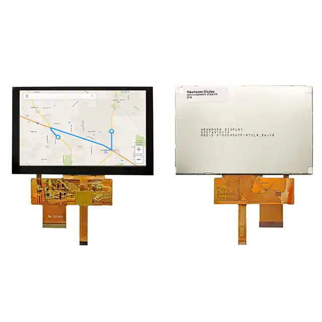


 工商网监
湘ICP备2023018690号
工商网监
湘ICP备2023018690号