NHD-C0216CZ-FSW-FBW-3V3 数据手册
NHD-C0216CZ-FSW-FBW-3V3
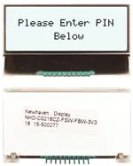
COG (Chip-on-Glass) Liquid Crystal Display Module
NHDC0216CZFSWFBW3V3-
Newhaven Display
COG, 2 Lines x 16 Characters
Model
Transflective
Side White LED Backlight
FSTN Positive.
6:00 Optimal View
Wide Temperature
3.3V LCD, 3V Backlight
RoHS Compliant
Newhaven Display International, Inc.
2661 Galvin Ct.
Elgin IL, 60124
Ph: 847-844-8795
Fax: 847-844-8796
www.newhavendisplay.com
nhtech@newhavendisplay.com
nhsales@newhavendisplay.com
�Document Revision History
Revision
0
1
2
3
4
5
6
7
8
9
10
11
12
13
14
15
Date
11/11/2008
8/26/2009
10/9/2009
10/22/2009
10/27/2009
11/19/2009
12/18/2009
3/2/2012
7/22/2013
12/10/2014
10/20/16
1/20/17
8/24/18
11/15/18
6/24/19
9/12/19
Description
Initial Release
User guide reformat
Updated Electrical Characteristics
Font Table Revision
Updated the Block Diagram
Updated backlight supply current
Pin description updated
Interface information updated
Electrical characteristics updated
Recommended connector information updated
Mechanical Drawing, Electrical & Optical Char. Updated
P/N Printed on Back of Display, Electrical Char. Updated
Supply Current Updated
Updated Font Table for CGRAM
Added PCB Footprint Drawing
Supply Current Updated
Functions and Features
•
•
•
•
•
2 lines x 16 characters
Built-in controller (ST7032)
5x8 dots with cursor
4-line serial interface
1/16 duty, 1/5 bias
[2]
Changed by
BE
MC
BE
MC
MC
BE
AK
ML
AK
SB
SB
SB
TM
AS
SB
�1
2
3
4
5
6
SYMBOL
7
8
REVISION
DATE
A
A
BLU 41.4±0.3
(1.9)
3±0.5
FRONT
0.6
34.6±0.2
Pin
Assignment
NO. Symbol
K
F
1
COM & SEG Layout
1/16 Duty, 1/5 Bias
FSTN Posi�ve / Transflec�ve
6:00
3.3V VDD, 5.5V VLCD
White LED
ST7032-0D
2
1
2
3
4
5
6
7
8
9
10
1.2±0.2
BACK
3
2.16
1.82
0.37
0.34
5
E
STANDARD TOLERANCE:
0.49
6
REVISION:
DRAWING/PART NUMBER:
1A
NHD-C0216CZ-FSW-FBW-3V3
UNLESS OTHERWISE SPECIFIED:
DRAWN BY:
- DIMENSIONS ARE IN MILLIMETERS
DRAWN DATE:
- THIRD ANGLE PROJECTION
4
D
(UNLESS OTHERWISE SPECIFIED)
LINEAR: ±0.3mm
4.63
4.13
0.52
Notes:
1. Driver:
2. Display Mode:
3. Op�mal View:
4. Voltage:
5. Backlight:
6. Driver IC:
C
3.4
FRONT
0.4
E
10
1
2.55
13.95±0.2
A
D
B
1
P1.5x9=13.5
40.2±0.2
1.2
0.6
(11.12)
(9.1)
10
0.6
0.3
0.75
UV Glue
BACK
FRONT
A.A8.76
V.A12.8MIN
Tear tape
Silicone
0.9
C
LCD 2.1 MAX.
(3.59)
7.6
LCD 22.5±0.2
BLU 24.3±0.3
B
LCD 15.8±0.2
A.A 34.22
4±0.3
0.9
23.1±0.2
V.A 37.6 MIN
BACK
0.9
4-Ø 0.8
LCD 39.6±0.2
S. Baxi
9/12/19
APPROVED BY:
SIZE:
A3
S. Baxi
SCALE:
APPROVED DATE:
DO NOT SCALE DRAWING
NS
9/12/19
SHEET 1 OF 1
THIS DRAWING IS SOLELY THE PROPERTY OF NEWHAVEN DISPLAY INTERNATIONAL, INC.
THE INFORMATION IT CONTAINS IS NOT TO BE DISCLOSED, REPRODUCED OR COPIED IN
WHOLE OR PART WITHOUT WRITTEN APPROVAL FROM NEWHAVEN DISPLAY.
7
8
F
�1
2
3
4
5
6
SYMBOL
A
7
8
REVISION
DATE
Recommended PCB Footprint
A
B
B
C
C
D
D
E
E
STANDARD TOLERANCE:
(UNLESS OTHERWISE SPECIFIED)
Applicable Displays:
1) NHD-C0216CZ-NSW-BBW-3V3
2) NHD-C0216CZ-FSW-FBW-3V3
LINEAR: ±0.3mm
DRAWN BY:
- DIMENSIONS ARE IN MILLIMETERS
DRAWN DATE:
- THIRD ANGLE PROJECTION
1
2
3
4
5
6
1.0
NHD-C0216CZ-Footprint
UNLESS OTHERWISE SPECIFIED:
F
REVISION:
DRAWING/PART NUMBER:
A. Shah
6/4/19
APPROVED BY:
APPROVED DATE:
DO NOT SCALE DRAWING
SIZE:
A3
A. Khan
SCALE:
NS
6/4/19
SHEET 1 OF 1
THIS DRAWING IS SOLELY THE PROPERTY OF NEWHAVEN DISPLAY INTERNATIONAL, INC.
THE INFORMATION IT CONTAINS IS NOT TO BE DISCLOSED, REPRODUCED OR COPIED IN
WHOLE OR PART WITHOUT WRITTEN APPROVAL FROM NEWHAVEN DISPLAY.
7
8
F
�Pin Description and Wiring Diagram
Pin No.
1
2
3
4
5
6
7
8
9
10
A
K
Symbol
RST
RS
CSB
SCL
SI
VSS
VDD
VOUT
C1+
C1LED+
LED-
External Connection
MPU
MPU
MPU
MPU
MPU
Power Supply
Power Supply
Power Supply
Function Description
Active LOW Reset Signal
Register Select Signal. RS=0: instruction; RS=1: data
Active LOW Chip Select signal
Serial Clock
Serial Input data
Ground
Power supply for logic for LCD (3.3V).
DC/DC voltage converter. Connect to 1uF capacitor to VDD or VSS
Voltage booster circuit. Connect to 0.47µF-2.2µF cap to PIN10.
Voltage booster circuit. Connect to 0.47µF-2.2µF cap to PIN9.
Backlight Anode (3.0V)
Backlight Cathode (Ground)
Recommended LCD connector: LCD pins should be soldered directly onto thru-hole connection on PCB
Backlight connector: Backlight pins should be soldered directly onto thru-hole connection on PCB
Recommended Breakout Board: NHD-PCB0216CZ
[5]
�Electrical Characteristics
Item
Operating Temperature Range
Storage Temperature Range
Supply Voltage
Supply Current
Supply for LCD (contrast)
“H” Level input
“L” Level input
“H” Level output
“L” Level output
Backlight Supply Voltage
Backlight Supply Current
Optical Characteristics
Optimal
Viewing
Angles
Contrast Ratio
Item
Top
Bottom
Left
Right
Response Time
Rise
Fall
Symbol
TOP
TST
VDD
IDD
VLCD
VIH
VIL
VOH
VOL
Condition
Absolute Max
Absolute Max
VDD = 3.3V
TOP = 25°C
-
Min.
-20
-30
3.0
40
5.2
1.9
VSS
0.75 * VDD
VSS
Typ.
3.3
170
5.5
-
Max.
+70
+80
3.6
300
5.8
VDD
0.8
VDD
0.8
Unit
⁰C
⁰C
V
µA
V
V
V
V
V
VLED
ILED
VLED = 3.1V
3.0
10
3.1
30
3.2
36
V
mA
Symbol
ϕY+
ϕYθXθX+
CR
TR
TF
Condition
Min.
2
-
Typ.
20
40
40
40
4
200
250
Max.
300
350
Unit
⁰
⁰
⁰
⁰
ms
ms
CR ≥ 2
TOP = 25°C
Controller Information
Built-in ST7032 Controller.
Please download specification at http://www.newhavendisplay.com/app_notes/ST7032.pdf
DDRAM Address
1 2 3 4 5 6 7 8 9 10 11 12 13 14 15 16
00 01 02 03 04 05 06 07 08 09 0A 0B 0C 0D 0E 0F
40 41 42 43 44 45 46 47 48 49 4A 4B 4C 4D 4E 4F
[6]
�Table of Commands
Instruction
Clear
Display
Instruction code
RS
R/W
DB7
0
0
0
Instruction Execution Time
Description
OSC=
380kHz
OSC =
540kHz
OSC=
700kHz
1
Write “20H” to DDRAM and set
DDRAM address to “00H” from
AC
1.08
ms
0.76
ms
0.59
ms
1.08
ms
0.76
ms
0.59
ms
DB6 DB5 DB4 DB3 DB2 DB1 DB0
0
0
0
0
0
0
Return
Home
0
0
0
0
0
0
0
0
1
X
Set DDRAM Address to “00H”
from AC and return cursor to its
original position if shifted. The
contents of DDRAM are not
changed.
Entry Mode
Set
0
0
0
0
0
0
0
1
I/D
S
Sets cursor move direction and
specifies display shift. These
parameters are performed
during data write and read.
26.3 µs
18.5 µs
14.3 µs
Display
ON/OFF
0
0
0
0
0
0
1
D
C
B
D=1: Entire display on
C=1: Cursor on
B=1: Blinking cursor on
26.3 µs
18.5 µs
14.3 µs
26.3 µs
18.5 µs
14.3 µs
26.3 µs
18.5 µs
14.3 µs
0
0
0
Function set
0
0
0
0
1
DL
N
DH
IS2
IS1
DL: Interface data is 8/4 bits
N: Number of lines is 2/1
DH: Double Height Font
IS 2~1: Instruction Table
Select
Set DDRAM
Address
0
0
1
AC6
AC5
AC4
AC3
AC2
AC1
AC0
Set DDRAM address in
address counter.
Whether during internal
operation or not can be known
by reading BF. The contents of
address counter can also be
read.
Read busy
Flag and
Address
Write data
To Address
Read data
From RAM
0
1
BF
AC6
AC5
AC4
AC3
AC2
AC1
AC0
1
0
D7
D6
D5
D4
D3
D2
D1
D0
Write data into internal RAM
(DDRAM/CGRAM).
26.3 µs
18.5 µs
14.3 µs
1
1
D7
D6
D5
D4
D3
D2
D1
D0
Read data from internal RAM
(DDRAM/CGRAM/ICONRAM).
26.3 µs
18.5 µs
14.3 µs
Sets cursor moving and display
shift control bit, and the
direction without changing
DDRAM data.
26.3 µs
18.5 µs
14.3 µs
Set CGRAM address in
address counter
26.3 µs
18.5 µs
14.3 µs
BS = 1 : 1/4 bias
BS= 0 : 1/5 bias
F2~0 : Adjust internal OSC
frequency for FR frequency
26.3 µs
18.5 µs
14.3 µs
Set ICON address in address
counter
26.3 µs
18.5 µs
14.3 µs
Ion: ICON display on/off
Bon: Set booster circuit on/off
C5,C4: Contrast set for internal
follower mode
26.3 µs
18.5 µs
14.3 µs
Fon: Set follower circuit on/off
Rab 2~0: select follower
amplified ratio
26.3 µs
18.5 µs
14.3 µs
Contrast set for internal
follower mode.
26.3 µs
18.5 µs
14.3 µs
Instruction Table 0 (IS[2:1] = [0,0]))
Cursor or
Display shift
0
0
0
0
0
1
S/C
R/L
X
X
Set CGRAM
0
0
0
1
AC5
AC4
AC3
AC2
AC1
AC0
Instruction Table 1 (IS[2:1] = [0,1]))
Internal OSC
Frequency
0
0
0
0
0
1
BS
F2
F1
F0
0
0
0
1
0
0
AC3
AC2
AC1
AC0
0
0
0
1
0
1
Ion
Bon
C5
C4
Follower
Control
0
0
0
1
1
0
Fon
Rab
2
Rab
1
Rab
0
Contrast Set
0
0
0
1
1
1
C3
C2
C1
C0
Set ICON
Address
Power/ICON
control/Cont
rast set
Instruction Table 2 ((IS[2:1] = [0,0]))
Double
Height
Position
Select
Reserved
0
0
0
0
0
1
UD
0
0
0
1
X
X
X
X
X
UD: Double height position
Select
26.3 µs
18.5 µs
14.3 µs
X
X
Do not use (Reserved for Test)
26.3 µs
18.5 µs
14.3 µs
X
X
*Instruction Table 3 (IS[2,1] = [1,1]): Do not use (Reserved for Test)
[7]
�Timing Characteristics
[8]
�Built-In Font Table
[9]
�Example Initialization Program
void init()
//initialize the LCD
{
P3 = 1;
P1 = 1;
RST = 0;
delay(2);
RST = 1;
delay(20);
Writecom(0x30);
delay(2);
Call writecom(0x30);
Call writecom(0x30);
Call writecom(0x39);
Call writecom(0x14);
Call writecom(0x56);
Call writecom(0x6D);
Call writecom(0x70);
Call writecom(0x0C);
Call writecom(0x06);
Call writecom(0x01);
delay(10);
}
//RESET
//end reset
//wake up
//wake up
//wake up
//function set
//internal osc frequency
//power control
//follower control
//contrast
//display on
//entry mode
//clear
void writecom(int d)
{
CS = 0;
//CS
RS = 0;
//A0 = Command
for(serialcounter = 1; serialcounter
NHD-C0216CZ-FSW-FBW-3V3 价格&库存
很抱歉,暂时无法提供与“NHD-C0216CZ-FSW-FBW-3V3”相匹配的价格&库存,您可以联系我们找货
免费人工找货