NHD-C160100AZ-RN-GBW 数据手册
NHD‐C160100AZ‐RN‐GBW
COG (Chip‐On‐Glass) Liquid Crystal Display Module
NHD‐ C160100‐ AZ‐ R‐ N‐ G‐ B‐ W‐ Newhaven Display 160 x 100 pixels Model Reflective No backlight STN‐ Gray 6:00 view Wide Temp (‐20°C ~ +70°C) RoHS Compliant
Newhaven Display International, Inc.
2511 Technology Drive, Suite 101 Elgin IL, 60124 Ph: 847‐844‐8795 Fax: 847‐844‐8796
www.newhavendisplay.com nhtech@newhavendisplay.com nhsales@newhavendisplay.com [1]
�Document Revision History
Revision 0 1 2 3 Date 10/31/2007 9/14/2009 10/14/2009 12/08/2009 Description Initial Release User guide reformat Updated Electrical Characteristic Updated Block Diagram, Pins 4 and 5, and Timing Characteristics Changed by ‐ BE MC MC
Functions and Features
• • • • • 160 x 100 pixels Built‐in ST7528 controller +3.0V power supply 1/100 duty; 1/11 bias RoHS Compliant
[2]
�Mechanical Drawing
PIN ASSIGNMENT
CSB 1 RST 2 A0 3 /WR 4 /RD 5 DB0 6 DB1 7 DB2 8 DB3 9 10 DB4 11 DB5 12 DB6 13 DB7 14 VDD 15 VSS 16 VOUT V4 17 V3 18 V2 19 V1 20
8
NHD-C160100AZ-RN-GBW
Newhaven Display
�Pin Description and Wiring Diagram
Pin No. Symbol 1 2 3 4 5 6‐13 14 15 16 17 18 19 20 CSB RST A0 /WR /RD DB0‐DB7 VDD Vss VOUT V4 V3 V2 V1 External Connection MPU MPU MPU MPU MPU MPU Power Supply Power Supply Power Supply Power Supply Power Supply Power Supply Power Supply Function Description Active Low chip select Active Low Reset signal Register select signal. A0=1: Data, A0=0: Command Active LOW write signal Active LOW read signal Bi‐directional 8‐bit data bus. Power supply for LCD and logic (+3.0V) Ground Connect to 1uF cap to VSS or VDD 1.0uF‐2.2uF cap to Vss 1.0uF‐2.2uF cap to Vss 1.0uF‐2.2uF cap to Vss 1.0uF‐2.2uF cap to Vss
Recommended LCD connector: 0.5mm pitch pins. Molex p/n: 52746‐2070 Backlight connector: ‐‐‐ Mates with: ‐‐‐
[4]
�Electrical Characteristics
Item Operating Temperature Range Storage Temperature Range Supply Voltage Supply Current Supply for LCD (contrast) “H” Level input “L” Level input “H” Level output “L” Level output Symbol Top Tst VDD IDD VDD‐V0 Vih Vil Voh Vol Condition Absolute Max Absolute Max Ta=25 , VDD=3.0V Ta=25 Min. ‐10 ‐20 2.8 ‐ ‐ 2.2 0 2.4 ‐ Typ. ‐ ‐ 3.0 1.5 11.5 ‐ ‐ ‐ ‐ Max. +60 +70 3.3 2.5 ‐ VDD 0.6 ‐ 0.4 Unit ⁰C ⁰C V mA V V V V V
Optical Characteristics
Item Viewing Angle ‐ Vertical Viewing Angle ‐ Horizontal Contrast Ratio Response Time (rise) Response Time (fall) Symbol θ Φ CR Tr Tf Condition Cr≥2 Min. ‐60 ‐40 ‐ ‐ ‐ Typ. ‐ 6 150 150 Max. +35 +40 ‐ 250 250 Unit ⁰ ⁰ ‐ ms ms
-
Controller Information
Built‐in ST7528. Download specification at http://www.newhavendisplay.com/app_notes/ST7528.pdf
[5]
�
[6]
�Table of Commands
[7]
�Example Initialization Program
//‐‐‐‐‐‐‐‐‐‐‐‐‐‐‐‐‐‐‐‐‐‐‐‐‐‐‐‐‐‐‐‐‐‐‐‐‐‐‐‐‐‐‐‐‐‐‐‐‐‐‐‐‐‐‐‐‐‐‐‐‐ void write_command(unsigned char datum) { A0=0; E=1; P1 = datum; CS1=0; RW=0; RW=1; CS1=1; } //‐‐‐‐‐‐‐‐‐‐‐‐‐‐‐‐‐‐‐‐‐‐‐‐‐‐‐‐‐‐‐‐‐‐‐‐‐‐‐‐‐‐‐‐‐‐‐‐‐‐‐‐‐‐‐‐‐‐‐‐‐ void write_data(unsigned char datum) { A0=1; E=1; P1=datum; CS1=0; RW=0; RW=1; CS1=1; } //‐‐‐‐‐‐‐‐‐‐‐‐‐‐‐‐‐‐‐‐‐‐‐‐‐‐‐‐‐‐‐‐‐‐‐‐‐‐‐‐‐‐‐‐‐‐‐‐‐‐‐‐‐‐‐‐‐‐‐‐‐ void lcd_init(void){ write_command(0xA2); //ICON OFF; write_command(0xAE); //Display OFF write_command(0x48); //Set Duty ratio write_command(0x80); //No operation write_command(0xa1); //Set scan direction //changed from 0 to 1 write_command(0xc8); //SHL select write_command(0x40); //Set START LINE write_command(0x00); write_command(0xab); //OSC on write_command(0x64); //3x delay(2000); write_command(0x65); //4x delay(2000); write_command(0x66); //5x delay(2000); write_command(0x67); //6x delay(2000); write_command(Ra_Rb); //RESISTER SET write_command(0x81); //Set electronic volume register write_command(vopcode); //n=0~3f write_command(0x57); //1/12bias write_command(0x92); //FRC and pwm write_command(0x2C); delay(20000);//200ms
/*Instruction register*/ /*Read inactive*/ /*put data on port 1*/ /*Chip select active*/ /*Write active*/ /*Write inactive; latch in data*/ /*Chip select inactive*/
/*DDRAM data register*/
[8]
� write_command(0x2E); delay(20000);//200ms write_command(0x2F); delay(20000);//200ms write_command(0x92); //frc and pwm write_command(0x38); //external mode write_command(0x75); //start settings for 16‐level grayscale write_command(0x97); //3frc,45pwm write_command(0x80); write_command(0x00); write_command(0x81); write_command(0x00); write_command(0x82); write_command(0x00); write_command(0x83); write_command(0x00); write_command(0x84); write_command(0x06); write_command(0x85); write_command(0x06); write_command(0x86); write_command(0x06); write_command(0x87); write_command(0x06); write_command(0x88); write_command(0x0b); write_command(0x89); write_command(0x0b); write_command(0x8a); write_command(0x0b); write_command(0x8b); write_command(0x0b); write_command(0x8c); write_command(0x10); write_command(0x8d); write_command(0x10); write_command(0x8e); write_command(0x10); write_command(0x8f); write_command(0x10); write_command(0x90); write_command(0x15); write_command(0x91); write_command(0x15); write_command(0x92); write_command(0x15); write_command(0x93); write_command(0x15); write_command(0x94); write_command(0x1a); write_command(0x95); write_command(0x1a); write_command(0x96); write_command(0x1a);
[9]
� write_command(0x97); write_command(0x1a); write_command(0x98); write_command(0x1e); write_command(0x99); write_command(0x1e); write_command(0x9a); write_command(0x1e); write_command(0x9b); write_command(0x1e); write_command(0x9c); write_command(0x23); write_command(0x9d); write_command(0x23); write_command(0x9e); write_command(0x23); write_command(0x9f); write_command(0x23); write_command(0xa0); write_command(0x27); write_command(0xa1); write_command(0x27); write_command(0xa2); write_command(0x27); write_command(0xa3); write_command(0x27); write_command(0xa4); write_command(0x2b); write_command(0xa5); write_command(0x2b); write_command(0xa6); write_command(0x2b); write_command(0xa7); write_command(0x2b); write_command(0xa8); write_command(0x2f); write_command(0xa9); write_command(0x2f); write_command(0xaa); write_command(0x2f); write_command(0xab); write_command(0x2f); write_command(0xac); write_command(0x32); write_command(0xad); write_command(0x32); write_command(0xae); write_command(0x32); write_command(0xaf); write_command(0x32); write_command(0xb0); write_command(0x35); write_command(0xb1); write_command(0x35); write_command(0xb2); write_command(0x35);
[10]
� write_command(0xb3); write_command(0x35); write_command(0xb4); write_command(0x38); write_command(0xb5); write_command(0x38); write_command(0xb6); write_command(0x38); write_command(0xb7); write_command(0x38); write_command(0xb8); write_command(0x3a); write_command(0xb9); write_command(0x3a); write_command(0xba); write_command(0x3a); write_command(0xbb); write_command(0x3a); write_command(0xbc); write_command(0x3c); write_command(0xbd); write_command(0x3c); write_command(0xbe); write_command(0x3c); write_command(0xbf); write_command(0x3c); //end settings for 16‐level grayscale write_command(0x38); write_command(0x74); write_command(0xaf); //Display ON } //‐‐‐‐‐‐‐‐‐‐‐‐‐‐‐‐‐‐‐‐‐‐‐‐‐‐‐‐‐‐‐‐‐‐‐‐‐‐‐‐‐‐‐‐‐‐‐‐‐‐‐‐‐‐‐‐‐‐‐‐‐
[11]
�Quality Information
Test Item
High Temperature storage Low Temperature storage High Temperature Operation Low Temperature Operation High Temperature / Humidity Operation Thermal Shock resistance
Content of Test
Endurance test applying the high storage temperature for a long time. Endurance test applying the low storage temperature for a long time. Endurance test applying the electric stress (voltage & current) and the high thermal stress for a long time. Endurance test applying the electric stress (voltage & current) and the low thermal stress for a long time. Endurance test applying the electric stress (voltage & current) and the high thermal with high humidity stress for a long time. Endurance test applying the electric stress (voltage & current) during a cycle of low and high thermal stress. Endurance test applying vibration to simulate transportation and use.
Test Condition
+70⁰C , 48hrs ‐20⁰C , 48hrs +60⁰C 48hrs
Note
2 1,2 2
‐10⁰C , 48hrs
1,2
+40⁰C , 90% RH , 48hrs
1,2
Vibration test
Static electricity test
Endurance test applying electric static discharge.
‐0⁰C,30min ‐> 25⁰C,5min ‐> 50⁰C,30min = 1 cycle 10 cycles 10‐55Hz , 15mm amplitude. 60 sec in each of 3 directions X,Y,Z For 15 minutes VS=800V, RS=1.5kΩ, CS=100pF One time
3
Note 1: No condensation to be observed. Note 2: Conducted after 4 hours of storage at 25⁰C, 0%RH. Note 3: Test performed on product itself, not inside a container.
Precautions for using LCDs/LCMs
See Precautions at www.newhavendisplay.com/specs/precautions.pdf
Warranty Information and Terms & Conditions
http://www.newhavendisplay.com/index.php?main_page=terms
[12]
�
NHD-C160100AZ-RN-GBW 价格&库存
很抱歉,暂时无法提供与“NHD-C160100AZ-RN-GBW”相匹配的价格&库存,您可以联系我们找货
免费人工找货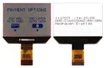


 工商网监
湘ICP备2023018690号
工商网监
湘ICP备2023018690号