NJM12856
LDO with Reverse Current Protection / Soft Start / Discharge Function
GENERAL DESCRIPTION
The NJM12856 is a low dropout regulator which achieves
high ripple rejection, low noise and high speed response with
the bipolar technology.
Adjustable soft-start function is useful for reducing inrush
current and controlling power-on sequence. Moreover the
discharge function makes effective sequence control with the
soft-start function.
In addition, the reverse current protection makes external
SBD unnecessary.
■
PACKAGE OUTLINE
NJM12856U2
NJM12856DL3
FEATURE
Operating Voltage Range 2.5V ~ 6.5V
Output Voltage Accuracy
VO 1.0%
Output Current
IO(min.)=1000mA
Reverse Current Protection
Adjustable soft-start Function
Discharge Function
ON/OFF Control
Correspond to Low ESR capacitor (MLCC)
Thermal Shutdown Circuit
Over Current Protection Circuit
Package Outline
SOT-89-5, TO-252-5
PIN CONFIGRATION
VOUT 1
5 VIN
GND 2
2 GND
CS 3
3
4 CONTROL
NJM12856U2
5
CS
4
VOUT
3
GND
2
VIN
CONTROL
1
NJM12856DL3
BLOCK DIAGRAM
VIN
CONTROL
VOUT
Reverse
Current
Protection
Thermal
Protection
CS
Bandgap
Reference
Over Current
Protection
GND
Ver.2015-07-21
-1-
�NJM12856
OUTPUT VOLTAGE RANK LIST
SOT-89-5
TO-252-5
Output
Device Name
Device Name
Voltage
NJM12856U2-15
1.5V
NJM12856DL3-15
NJM12856U2-18
1.8V
NJM12856DL3-18
NJM12856U2-25
2.5V
NJM12856DL3-25
NJM12856U2-33
3.3V
NJM12856DL3-33
NJM12856U2-05
5.0V
NJM12856DL3-05
ABSOLUTE MAXIMUM RATINGS
PARAMETER
SYMBOL
Input Voltage
VIN
Control Pin Voltage
VCONT
Output Voltage
VOUT
Soft start Pin Voltage
VCS
Power Dissipation
PD
Junction Temperature Range
Operating Temperature Range
Storage Temperature Range
Tj
Topr
Tstg
Output
Voltage
1.5V
1.8V
2.5V
3.3V
5.0V
(Ta=25 C)
MAXIMUM RATING
UNIT
-0.3 ~ +7
-0.3 ~ +7
-0.3 ~ +5.5
Vo 1.8V
-0.3 ~ +7
Vo 1.8V
-0.3 ~ +2.5
625(*1)
SOT-89-5
2400(*2)
1190(*1)
TO-252-5
3125(*2)
-40 +150
-40 +125
-50 +150
V
V
V
V
V
mW
C
C
C
2
(*1): Mounted on glass epoxy board. (76.2 114.3 1.6mm:based on EIA/JDEC standard size, 2Layers, Cu area 100mm )
(*2): Mounted on glass epoxy board. (76.2 114.3 1.6mm:based on EIA/JDEC standard, 4Layers)
(For 4Layers: Applying 74.2 74.2mm inner Cu area and a thermal via hole to a board based on JEDEC standard JESD51-5)
Operating Voltage Range :VIN=2.5V ~ 6.5V
-2-
Ver.2015-07-21
�NJM12856
ELECTRICAL CHARACTERISTICS
(Unless other noted,
VIN = VO + 1V, CIN = 0.33µF, CO =0.47µF(CO=1.0µF :2.4V Vo 2.9V, CO=2.2µF :1.7V Vo 2.4V, Co=4.7µF :Vo 1.7V), Cs=0.01µF, Ta = 25°C)
PARAMETER
SYMBOL
TEST CONDITION
MIN.
TYP.
MAX.
UNIT
-1.0%
-
+1.0%
V
Output Voltage
VO
IO=200mA
Quiescent Current
IQ
IO = 0mA, except ICONT
-
400
600
μA
Quiescent Current
at OFF-state
IQ(OFF)
VCONT = 0V
-
-
10
μA
1000
-
-
mA
Output Current
IO
Line Regulation
VO/ VIN
VIN = VO + 1V ~ 6.5V, Io=200mA
-
-
0.15
%/V
Load Regulation
VO/ IO
IO = 0 ~ 1000mA
-
-
0.003
%/mA
IO=600mA
-
0.20
0.28
V
Ta= -40 ~ +125 C, IO=200mA
-
50
-
ppm/ C
VIN =3.0V
ein=200mVrms,
f=1kHz, Io=10mA
Vo=1.5V
-
78
-
Vo=1.8V
-
76
-
Vo=2.5V
-
73
-
Vo=3.3V
-
72
-
Vo=5.0V
-
68
-
Vo=1.5V
-
17
-
Vo=1.8V
-
19
-
Vo=2.5V
-
24
-
Vo=3.3V
-
30
-
Vo=5.0V
-
42
-
-
3
12
μA
VCONT(ON)
1.6
-
-
V
VCONT(OFF)
-
-
0.6
V
VCONT=L→H, Io=200mA, Cs=0.022μF
-
1.2
-
msec
VIN=2.5V, VCONT=0V, VO =0.5V
3
10
VIN=6.5V, VCONT=0V, VO =0.5V
15
25
Dropout Voltage (*3)
Average Temperature
Coefficient of Output Voltage
Ripple Rejection
VIO
VO/ Ta
VO 0.9
RR
ein=200mVrms,
f=1kHz, Io=10mA
Output Noise Voltage
Control Current
Control Voltage at
ON-state
Control Voltage at
OFF-state
Soft Start Time
Discharge Current
at OFF-state
VNO
ICONT
tS(ON)
IDIS
f=10Hz ~ 80kHz,
Io=10mA
VCONT =1.6V
dB
μVrms
mA
(*3): Except Output Voltage Rank less than 2.2V
The above specification is a common specification for all output voltages.
Therefore, it may be different from the individual specification for a specific output voltage.
Ver.2015-07-21
-3-
�NJM12856
POWER DISSIPATION vs. AMBIENT TEMPERATURE
NJM12856U2 PowerDissipation
Power Dissipation PD(mW)
(Topr=-40~+125°C,Tj=150°C)
3000
on 4 layers board
2500
2000
1500
1000
on 2 layers board
500
0
-50
-25
0
25
50
75
100
125
150
100
125
150
Temperature : Ta(°C)
NJM12856DL3 PowerDissipation
(Topr=-40~+125°C,Tj=150°C)
Power Dissipation PD(mW)
3500
3000
on 4 layers board
2500
2000
1500
1000
on 2 layers board
500
0
-50
-25
0
25
50
75
Temperature : Ta(°C)
TEST CIRCUIT
A
VIN
IIN
VIN
0.33μF
VOUT
(*4)
0.47μF
NJM12856
(ceramic)
A
V VCONT
ICONT
IOUT V VOUT
(ceramic)
CONTROL
GND
Cs
0.01μF
(ceramic)
*4: 2.4V
很抱歉,暂时无法提供与“NJM12856U2-18-TE1”相匹配的价格&库存,您可以联系我们找货
免费人工找货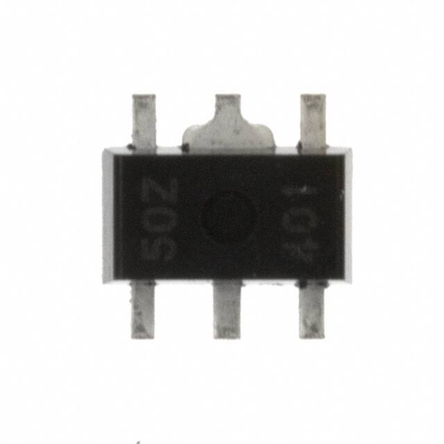


 工商网监
湘ICP备2023018690号
工商网监
湘ICP备2023018690号
