NJU7074M

NJU7074M

  • 厂商:

    NJRC

  • 封装:

    LSSOP14

  • 描述:

    IC OPAMP GP 4 CIRCUIT 14DMP

  • 详情介绍
  • 数据手册
  • 价格&库存
NJU7074M 数据手册
NJU7071/72/74 LOW INPUT OFFSET VOLTAGE C-MOS OPERATIONAL AMPLIFIER ■ GENERAL DESCRIPTION The NJU7071,72 and 74 are single, dual and quad C-MOS Operational Amplifiers operated on a single-power-supply and low operating current. The input offset voltage is lower than 2mV,and the input bias current is as low as less than 1pA,consequently the very small single around the ground level can be amplified. The minimum operating voltage is 5V and the output stage permits output signal to swing between both of the supply rails. Furthermore, the operating current is also as low as 0.6mA ( typ. ) per circuit, therefore it can be applied especially to battery-operated items. ■ FEATURES ● Single-Power-Supply ● Low Input Offset Voltage ( VIO=2mV max ) ● Wide Operating Voltage ( VDD=5~16V ) ● Wide Output Swing Range ( VOM≥9.98V typ. @ VDD=10V ) ● Low Operating Current ( 0.6mA/circuit typ. ) ● Low Bias Current ( IIB=1pA typ. ) ● Internal Compensation Capacitor ● External Offset Null Adjustment ( Only NJU7071 ) ● Package Outline DIP/DMP/SSOP8 ( NJU7071 ) DIP/DMP8 ( NJU7072 ) DIP/DMP/SSOP14 ( NJU7074 ) ● C-MOS Technology ■ PIN CONFIGURATION ■ PACKAGE OUTLINE NJU7071D NJU7072D NJU7071M NJU7072M NJU7074D NJU7074M NJU7071V NJU7074V NJU7071D NJU7071M NJU7071V NJU7072D NJU7072M NJU7074D NJU7074M NJU7074V Ver.2003-03-18 -1- NJU7071/72/74 ■ EQUIVALENT CIRCUIT ‫٭‬The terminals IN1, IN2 are only for NJU7071 ( NJU7072/74 don’t have these terminals ). -2- Ver.2003-03-18 NJU7071/72/74 ■ ABSOLUTE MAXIMUM RATINGS ( Ta=25˚C ) PARAMETER Supply Voltage Differential Input Voltage Common Mode Input Voltage Power Dissipation SYMBOL VDD VID VIC PD Topr Tstg RATINGS 18 ± 18 ( note1 ) -0.3~18 ( DIP8 ) 500 ( DIP14 ) 700 ( DMP8,14 ) 300 ( SSOP8 ) 250 ( SSOP14 ) 300 -20~+75 -40~+125 UNIT V V mA mW Operating Temperature Range Storage Temperature Range ˚C ˚C ( note1 ) If the supply voltage ( VDD ) is less than 18V, the input voltage must not over the VDD level though 18V is limit specified. ■ ELECTRICAL CHARACTERISTICS ( Ta=25˚C,VDD=10V,RL=∞ ) PARAMETER Input Offset Voltage Input Offset Current Input Bias Current Input Impedance Large Signal Voltage Gain Input Common Mode Voltage Range Maximum Output Swing Voltage Common Mode Rejection Ratio Supply Voltage Rejection Ratio Operating Current/Circuit Slew Rate Unity Gain Bandwidth SYMBOL VIO IIO IIB RIN AV VICM VOM CMR SVR IDD SR Ft TEST CONDITION RS=50Ω MIN. 80 0~9 9.80 60 60 TYP. 1 1 1 95 9.98 75 75 0.6 1.1 1.0 MAX. 2 1.2 UNIT mV pA pA TΩ dB V V dB dB mA V/µs MHz RL=1MΩ AV=40dB,CL=10pF ■ OFFSET ADJUSTMENT CIRCUIT ( Only For NJU7071 ) [CAUTION] The specifications on this databook are only given for information , without any guarantee as regards either mistakes or omissions. The application circuits in this databook are described only to show representative usages of the product and not intended for the guarantee or permission of any right including the industrial rights. Ver.2003-03-18 -3-
NJU7074M
### 物料型号 - NJU7071:单通道C-MOS运算放大器 - NJU7072:双通道C-MOS运算放大器 - NJU7074:四通道C-MOS运算放大器

### 器件简介 NJU7071、NJU7072和NJU7074是单电源供电、低工作电流的C-MOS运算放大器。它们具有低输入偏置电压(小于2mV)和低输入偏置电流(小于1pA),能够放大围绕地电平的非常小的信号。最低工作电压为5V,输出级允许输出信号在供电轨之间摆动。每个电路的工作电流低至0.6mA(典型值),适用于电池供电设备。

### 引脚分配 - NJU7071D、NJU7071M、NJU7071V:单通道,8引脚封装 - NJU7072D、NJU7072M:双通道,8引脚封装 - 
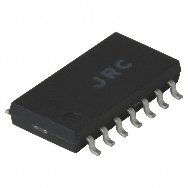
NJU7074D、NJU7074M、NJU7074V:四通道,14引脚封装

### 参数特性 - 单电源供电 - 低输入偏置电压(最大2mV) - 宽工作电压范围(5V至16V) - 宽输出摆动范围 - 低工作电流(每个电路0.6mA典型值) - 低偏置电流(1pA典型值) - 内部补偿电容 - 外部偏置调整(仅限NJU7071) - C-MOS技术

### 功能详解 这些运算放大器的主要功能是放大差分信号,具有低输入偏置电压和电流,适合电池供电应用。它们还具有内部补偿和外部偏置调整功能,以提高灵活性和精确度。

### 应用信息 适用于电池供电设备,以及其他需要低功耗、低输入偏置电压和电流的场合。

### 封装信息 - NJU7071:DIP/DMP/SSOP8封装 - NJU7072:DIP/DMP8封装 - NJU7074:DIP/DMP/SSOP14封装
NJU7074M 价格&库存

很抱歉,暂时无法提供与“NJU7074M”相匹配的价格&库存,您可以联系我们找货

免费人工找货