Toggles
OLED Rocker
DISTINCTIVE CHARACTERISTICS
Rockers
• Organic LED technology in display rocker
• Multi-function programmable device: select with rocker, push for activation
• Broad display aids in navigation, both forward and reverse and up and down, in structured menus
• Wide viewing angle of 180° and large 0.92” display with exceptional contrast
• Conforms to IP64 of IEC 60529 Standards on panel surface; dust tight construction of switch prevents
entry of dust and improves contact reliability
• Commands and data supplied via serial communications protocol (SPI)
• Long life OLED with 52,000 hours at 30% illumination
E
• High reliability and long mechanical and electrical life of one million actuations minimum
Keylocks
• Stylish black housing design with matte finish complements any application
Programmable Illuminated PB
Pushbuttons
• Replaces multiple switches and displays with one device in a small package
Rotaries
Monochrome OLED featuring sharp contrast and
high resolution with 96 x 64 pixels
Slides
Panel mount with easy, snap-in installation
Tactiles
Short 14.6mm (.575”) behind-panel height
for compact spaces
Touch
Tilt
Actual Size
Description
Accessories
Part Number
Indicators
SWITCH PART NUMBER & DESCRIPTION
OLED Rocker Switch: SP3T Switch
Rocker (ON) (ON) (ON)
Pushbutton Normally OFF
Supplement
IS18WWC1W
www.nkkswitches.com
E15
03/16/20
�Toggles
OLED Rocker
SWITCH SPECIFICATIONS
Circuit
Slides
Rotaries
Keylocks
Programmable Illuminated PB
Pushbuttons
Rockers
Contact Position
E
Contact Resistance
200 milliohms maximum
Insulation Resistance
500 megohms minimum @ 250V DC
Dielectric Strength
250V AC for 1 minute minimum
Electrostatic Resisting Pressure
15kV minimum
Mechanical Endurance
1,000,000 operations minimum
Electrical Endurance
1,000,000 operations minimum
Operating Force
5± 2 Newtons at center of cap; 3.7± 1.7 Newtons at top and bottom
Total Travel
1.3± 0.5mm (.051”± .020") at center of cap; 1.8± 0.6mm (.071”±.024") at top and bottom
OLED SPECIFICATIONS
Characteristics of Display
Display Device
Single color OLED display
Display Mode
Passive matrix
Pixel Format
96 x 64 pixels (horizontal x vertical)
Pixel Size
0.16mm x 0.177mm (horizontal x vertical)
Interface
Serial (SPI) interface
Color
White/Black (normally White)
Splash & Dust Proof
Conforms to IP64 of IEC60529 standards on panel surface
Operating Temperature Range
–20°C ~ +70°C (–4°F ~ +158°F)
Storage Temperature Range
–25°C ~ +80°C (–13°F ~ +176°F)
Operating Life Time (Display)
52,000 hours (30% brightness); 15,600 hours (100% brightness)
Absolute Maximum Ratings (Temperature at 25°C)
Symbols
Recommended Operating Conditions
Ratings
Items
Symbols
Minimum
Typical
Maximum
VDDA
2.7V
2.8V
3.6V
Supply Voltage for Drive
VAH
14.5V
15.0V
15.5V
Input High Level Voltage
VI H
0.75 x VDDA
––
VDDA
Input Low Level Voltage
VI L
0.0
––
0.25V x VDDA
VI H
0.80 x VDDA
––
VDDA
VI L
0.0
––
0.20V x VDDA
Supply Voltage for
Logic/Interface
VDDA
–0.3V to +3.6V
Supply Voltage for
Logic/Interface
Supply Voltage for Drive
VAH
–0.3V to +18.0V
Input Voltage
Vin
–0.3V to VDDA +0.3V
Tilt
Touch
Indicators
Accessories
Down
(ON) 11-12
3VA maximum @ 24V DC maximum
(Applicable Range 10mA ~ 125mA @ 0.1V ~ 24V DC)
Input High Level Voltage
(XRES only)
Input Low Level Voltage
(XRES only)
Current Consumption
(Temperature at 25°C, VDDA = 2.8V, VAH = 15.0V)
Items
Supplement
Bottom
Normal
OFF
Electrical Capacity (Resistive Load)
Items
Tactiles
Single Pole Three Throw (Momentary)
Top
Center
Normal
Down
Normal
Down
OFF
(ON) 9-12
OFF
(ON) 10-12
Optical Characteristics
Symbols Min Typical
Max
––
8.3mA
All-Pixels-On Mode
*Drive System Power Current
I H1
All-Pixels-On Mode
*Logic/IF System Power Current
I DD1
Sleep Mode
**Drive System Power Current
I H2
––
––
10μA
Sleep Mode
**Logic/IF System Power Current
I DD2
––
––
10μA
6.9mA
Items
Brightness
––
0.3mA 0.36mA
Chromaticity
Contrast
* All pixels shall be turned on with the maximum level gray scale
** All pixels shall be turned off (while chip is operating)
E16
(Temperature at 25°C, Initial Value: depends on initial setting)
Minimum
Typical
75 cd/m
100 cd/m
2
Maximum
2
125 cd/m2
(x)
***2
0.310
***2
(y)
***2
0.330
***2
100
––
––
*** Chromaticity range is the area of the ellipse. (See Chromaticity Diagram
next page.) The ellipse passes through points A, B, C and D and
designates the center of each side of the quadrangle.
www.nkkswitches.com
�0.39
0.3105
D
0.3193
0.3088
TIMING SPECIFICATIONS
AC Characteristics
(Temperature at –20°C ~ +70°C), VDDA = 2.8V, VAH = 16V
Symbols Minimum Typical Maximum
Items
Clock Cycle Time
t c yc le
100ns
––
––
A0 Setup Time
t SWDS
65ns
––
––
A0 Hold Time
t SWDH
35ns
––
––
XCS Setup Time
t CWS
65ns
––
––
XCS Hold Time
t CWH
35ns
––
––
High Level XCS Pulse Width
t CSBH
*30ns
––
––
Rockers
0.3552
0.2561
D
C
0.25
0.27
0.29 0.31 0.33
Chromaticity X
0.35
Pushbuttons
0.3007
0.37
A0
tSWDS
t SWDH
t C WS
t CWH
XCS
E
tCSBH
tR
Write Data Setup Time
t WDTS
10ns
––
––
Write Data Hold Time
t WDTH
30ns
––
––
SCL Low Time
t SCLL
45ns
––
––
SCL High Time
t SCLH
45ns
––
––
SCL Rise Time
tr
––
––
15ns
SCL Fall Time
tf
––
––
15ns
t SC L H
t c yc le
SCL
tF
t SC L L
t WDTS
SI
t WDTH
D7
* Requires more than 100ns after resetting software
D6
D5
D4
D3
D2
D1
D0
Black & White OLED Panel
96 x 64
SEG1 . . . SEG96 COM1 . . . COM64
BLOCK DIAGRAM & PIN CONFIGURATIONS
Segment Driver
VDDA 1
VAH 8
XRES 2
SCL
XCS
SI
A0
5
3
6
4
Common Driver
OLED Driver
with Controller
Light Decoder
Display Control
& Screen Saver
Graphic Display
Data
RAM
128 x 64 x 1 Bit
I/F Circuit Block
Programmable Illuminated PB
B
C
A
B
Keylocks
0.3535
Rotaries
Chromaticity Y
0.3639
Oscillator
Timing
Control
Tactiles
Chromaticity X
A
Chromaticity Y
Point
0.38
0.37
0.36
0.35
0.34
0.33
0.32
0.31
0.30
0.29
0.28
0.27
0.26
0.25
Slides
Chromaticity Diagram
Toggles
OLED Rocker
Register
5
6
SCL
SI
VSS
VAH
SW1
SW2
SW3
SW_COM
7
8
9
10
11
12
A0
Logic Type Power Source
Reset
Chip Select
Touch
VDDA
XRES
XCS
Function
Terminal to initialize IC built-in logic; initializes with low level
Slave select for SPI. This line is active low.
Address
Terminal to input control signals of command/parameter
Set low at time of command input and high level at the time
of parameter input.
Serial Clock
Serial Data Input
Ground
Drive Type Power Source
Switch Terminal 1
Switch Terminal 2
Switch Terminal 3
Switch Common Terminal
Read command/parameter at time of SCL signal standing up
Terminal to input command/parameter by SPI
Indicators
1
2
3
4
Name
Accessories
Symbol
N/O
N/O
N/O
www.nkkswitches.com
Supplement
Pin No.
9 SW1
10 SW2
11 SW3
SW_COM 12
IS18WWC1W
Tilt
VSS 7
E17
�Toggles
OLED Rocker
TYPICAL SWITCH DIMENSIONS
(21.8)
.858
Pushbuttons
(38.8)
1.528
(13.22)
.520
(15.3)
.602
(50.7)
1.996
E
NKK P/N
This Side
(30.6)
1.205
(46.7)
1.839
(35.1)
1.382
(2.0)
.079
(37.9)
1.492
Keylocks
Programmable Illuminated PB
(35.4)
1.394
(19.16)
.754
Rockers
See
Pixel Detail
(0.8)
.031
(5.6)
.220
(14.6)
.575
(34.9)
1.374
12
11
10
(0.04) Typ
.0016
Rotaries
(0.16) Typ
.0063
Panel Thickness Range
Slides
(0.177) Typ
.0070
(0.03) Typ
.0012
3
2
1
Terminal Connector Detail
Tactiles
Pixel Detail
(48.6)
1.913
.039 ~ .157"
(1.0mm ~ 4.0mm)
(35.4)
1.394
Tilt
STATE TRANSITION
State 0
Power OFF
(VAH, VDDA OFF)
2 : Power OFF
8 : Initialization
Touch
7 : Power OFF
6 : VAH ON
State 0
1 : Power ON, Initialization
State 1
Display OFF
(Sleep Mode)
5 : VAH OFF
Initialization Setting
3 : Display ON
9 : Changing the Display
VDDA
4 : Display OFF
State
Number
E18
State
9 : Changing the Display
Display Sleep
VAH
9 : Changing the Display
VDDA
Power ON
State 1 ( State 3)
State 2
Power OFF
2.5V
State 2
Display ON
XRES
Supplement
Accessories
Indicators
State 3
Power Saver
Mode
Power ON/OFF Sequence
Changing
the Display
0
Power OFF
OFF
––
OFF
OFF
Disable
1
Display OFF
OFF
ON
ON
ON
Enable
2
Display ON
ON
OFF
ON
ON
Enable
3
Power Saver
OFF
ON
OFF
ON
Enable
2.5V
0V
Reset low pulse width
Trw (minimum 1µs)
“L”
www.nkkswitches.com
Waiting time for oscillation
stability (about 1.1ms)
(VDDA x 0.8)V
Completion time of reset Tr (minimum 0.1µs)
Waiting time to stabilize
VAH Level
VAH voltage: 1s (reference)
Minimum 0µs
0µs min
“L”
A0
“L”
SCL/SI
Reset low pulse width
Trw (minimum 1µs)
(VDDA x 0.2)V
Minimum 0µs
Waiting time to stabilize VAH
voltage: 1ms (reference)
VAH
0V
XCS
State 0
“Hi-z”
0µs min
“H” or “L”
“H” or “L”
“H” or “L”
�Toggles
OLED Rocker
STATE TRANSITION (CONTINUED)
5
VAH OFF
6
VAH ON
7
Power OFF
Display
ON
OFF
Minimum 10ms
ON
Wait until VAH becomes stable
Standby
OFF
Refer to "Power ON/OFF Sequence"
Initialization
Minimum 0µs
Waiting time to stabilize VAH
voltage: 1ms (Reference)
Minimum 0µs
VAH
Refer to "Initialization Setting"
Image
9
2.8V
Minimum 0µs
15V
0V
E
96 x 64 Image Data Sending
Display
Rewriting
Change
Display
Dimmer/Screen Saver/Indication
Settings
180° Reversal
Keylocks
8
Rockers
Display OFF
VDDA
INITIALIZITION SETTING
Command Name
Command Parameter
Remarks
Address (1 or 2Byte)
Software Reset
01
Dot Matrix Display ON/OFF
02
00
Read/Write Operation Wetting
07
Display Direction Set Command
Command Name
Command Parameter
Remarks
Address (1 or 2Byte)
38
00
Note 1
Note 1
Y Axis Reading Start Address
39
00
Note 1
00
Note 1
Reserved 9
48
03
Note 2
09
00
Note 1
Reserved 1
10
03
Note 2
Screen Saver Event Timer Setting
Command
C3
00
Note 1
Reserved 2
12
63
Note 2
C4
00
Note 1
Reserved 3
13
00
Note 2
Screen Saver Event Timer Setting
Command
Dot Matrix Display Standby ON/OFF
14
00
One Time, Repeat or Direction
Setting for Screen Saver
CC
00
Note 1
Reserved 4
16
00
Note 2
Start/Stop Setting for Screen Saver
CD
00
Note 1
Reserved 5
17
00
Notes 1 & 2
System Clock Division Ratio Setting
D0
80
Note 2
Reserved 6
18
09
Note 2
Reserved 7
1A
04
Notes 1 & 2
Setting the STBY Pin
D2
00
Notes 1 & 2
Reserved 8
1C
00
Notes 1 & 2
DACA Setting
D4
00
Note 2
Graphic Memory Writing Direction
1D
00
Note 1
DACB Setting
D5
00
Note 2
Setting Column Output Range
30
005F
Note 1
DACC Setting
D6
00
Note 2
Setting Row Output Range
32
003F
Note 1
DACD Setting
D7
00
Note 2
X Axis Reading/Writing Start Point
34
00
Note 1
Reserved 10
D9
00
Notes 1 & 2
X Axis Reading/Writing End Point
35
0B
Note 1
Dimmer Setting
DB
0F
Note 1
Y Axis Reading/WritingStart Point
36
00
Note 1
Reserved 11
DD
88
Note 2
Y Axis Reading/Writing End Point
37
3F
Note 1
Image Writing
08
Image data
2. Do not change setting value
Supplement
X Axis Reading Start Address
Notes: 1. Same as default value
Pushbuttons
4
Refer to
"Display ON/OFF Sequence"
Programmable Illuminated PB
Display ON
State 2 Display State 1 VAH OFF State 3 VAH ON State 1 Display State 2
OFF
ON
Notes: 1. Same as default value
2. Do not change setting value
www.nkkswitches.com
Rotaries
3
Refer to "Initialization Setting"
Refer to "Power ON/OFF Sequence"
Slides
Power OFF
Display ON/OFF Sequence
Tactiles
2
Refer to "Power ON/OFF Sequence"
Tilt
Power ON
Touch
1
Reference or Setting Procedure
Indicators
Transition
Accessories
State
Transition
E19
�Toggles
OLED Rocker
ACCESSORIES
(500.0) +50.0
– 0.0
19.685
PRECAUTIONS FOR HANDLING & STORAGE OF OLED ROCKERS
E
Handling
ATTENTION
ELECTROSTATIC
SENSITIVE DEVICES
1. OLED devices are electrostatic sensitive.
2. Signal input under conditions not recommended may cause damage to the OLED unit or deterioration of the display.
Follow directions regarding supply sequences of power and signal voltages.
Keylocks
Programmable Illuminated PB
Pushbuttons
Rockers
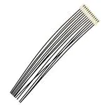
AT715 Cable for Connection
3. If the OLED panel is broken, avoid touching the contents. Wash off in case of contact to the skin or clothing.
Rotaries
4. Limit operating force to 100.0N maximum, as excessive pressure may damage the display.
5. Under certain actuation conditions, one side of the rocker and the center switch can both send actuation signals.
Slides
6. Pixels acquire diminished brightness over time and use, and those most frequently habituated have greater reduction of
brightness than those less used. To minimize this difference, operate OLED unit so that all pixels are used as consistently
as possible.
7. Clean actuator surface with dry cloth. If further cleaning is needed, wipe with dampened cloth using neutral cleanser and
dry with clean cloth. Do not use organic solvent.
Tactiles
Storage
1. Store in original container and away from direct sunlight.
2. Keep away from static electricity.
Tilt
3. Avoid extreme temperatures, high humidity, gaseous substances, and all forms of chemical contamination.
Incorrect
Correct
Gasket position must be even with no gaps beneath bezel
Gasket secure and flush against bezel
Panel Mounting
Touch
• Before snapping a switch into the panel, align the
gasket evenly under the bezel of the switch.
Indicators
• When mounting into a panel, apply equal pressure
to sides of bezel and insert parallel to the panel.
• After mounting, be sure there are no gaps between switch and panel. Lightly push into panel.
• After installing into panel, do not apply excessive force.
Accessories
• After panel installation and wiring is completed, do not apply force horizontally or
vertically from behind panel.
• Behind the panel, cut area should be squared. If front of panel is painted, do not allow any paint
to collect in corners of cutout to prevent level mounting.
Supplement
• Avoid reinstalling a switch once it has been mounted into panel. This may cause deterioration of
panel sealability.
E20
www.nkkswitches.com
Clean Edges
�
很抱歉,暂时无法提供与“AT715”相匹配的价格&库存,您可以联系我们找货
免费人工找货- 国内价格 香港价格
- 1+120.738441+15.14040
- 4+118.968084+14.91840
- 10+117.8173510+14.77410
- 25+116.6666225+14.62980
- 40+114.9847840+14.41890
- 国内价格 香港价格
- 1+80.728341+10.12320
- 5+79.666135+9.99000
- 20+78.6924320+9.86790
- 50+78.0728150+9.79020
- 125+76.92207125+9.64590
- 国内价格 香港价格
- 1+162.786781+20.41320
- 10+147.3957610+18.48319
- 25+141.6893225+17.76761
- 50+137.5203050+17.24482
- 100+133.47118100+16.73707
- 250+128.30034250+16.08865
- 500+124.52078500+15.61470


 工商网监
湘ICP备2023018690号
工商网监
湘ICP备2023018690号