CD4093BM CD4093BC Quad 2-Input NAND Schmitt Trigger
February 1993
CD4093BM CD4093BC Quad 2-Input NAND Schmitt Trigger
General Description
The CD4093B consists of four Schmitt-trigger circuits Each circuit functions as a 2-input NAND gate with Schmitt-trigger action on both inputs The gate switches at different points for positive and negative-going signals The difference between the positive (VT a ) and the negative voltage (VTb) is defined as hysteresis voltage (VH) All outputs have equal source and sink currents and conform to standard B-series output drive (see Static Electrical Characteristics)
Y Y Y Y
Equal source and sink currents No limit on input rise and fall time Standard B-series output drive Hysteresis voltage (any input) TA e 25 C VH e 1 5V Typical VDD e 5 0V VDD e 10V VH e 2 2V VDD e 15V VH e 2 7V Guaranteed VH e 0 1 VDD
Applications
Y Y Y Y Y
Features
Y Y
Y
Wide supply voltage range Schmitt-trigger on each input with no external components Noise immunity greater than 50%
3 0V to 15V
Wave and pulse shapers High-noise-environment systems Monostable multivibrators Astable multivibrators NAND logic
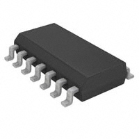
Connection Diagram
Dual-In-Line Package
TL F 5982 – 1
Top View Order Number CD4093B
C1995 National Semiconductor Corporation
TL F 5982
RRD-B30M105 Printed in U S A
�Absolute Maximum Ratings (Notes 1
2)
If Military Aerospace specified devices are required please contact the National Semiconductor Sales Office Distributors for availability and specifications DC Supply Voltage (VDD) Input Voltage (VIN) Storage Temperature Range (TS) Power Dissipation (PD) Dual-In-Line Small Outline Lead Temperature (TL) (Soldering 10 seconds)
b 0 5 to a 18 VDC b 0 5 to VDD a 0 5 VDC b 65 C to a 150 C
Recommended Operating Conditions (Note 2)
DC Supply Voltage (VDD) Input Voltage (VIN) Operating Temperature Range (TA) CD4093BM CD4093BC 3 to 15 VDC 0 to VDD VDC
b 55 C to a 125 C b 40 C to a 85 C
700 mW 500 mW 260 C
DC Electrical Characteristics CD4093BM (Note 2)
Symbol IDD Parameter Quiescent Device Current Low Level Output Voltage Conditions VDD e 5V VDD e 10V VDD e 15V VIN e VDD lIOl k 1 mA VDD e 5V VDD e 10V VDD e 15V VIN e VSS lIOl k 1 mA VDD e 5V VDD e 10V VDD e 15V 4 95 9 95 14 95 13 2 85 4 35 2 75 55 8 25 05 10 15 0 64 16 42
b 0 64 b1 6 b4 2 b0 1 b 55 C a 25 C a 125 C
Units mA mA mA V V V V V V
Min
Max 0 25 05 10 0 05 0 05 0 05
Min
Typ
Max 0 25 05 10
Min
Max 75 15 0 30 0 0 05 0 05 0 05
VOL
0 0 0 4 95 9 95 14 95 5 10 15 18 41 63 33 62 90 15 22 27 0 88 2 25 88
b 0 88 b 2 25 b8 8 b 10 b 5
0 05 0 05 0 05 4 95 9 95 14 95 2 25 45 6 75 35 70 10 5 20 40 60 15 30 45 2 65 5 35 81 0 35 0 70 1 20 0 36 09 24
b 0 36 b0 9 b2 4 b0 1
VOH
High Level Output Voltage
VTb
Negative-Going Threshold Voltage (Any Input)
l IO l k 1 m A VDD e 5V VO e 4 5V VDD e 10V VO e 9V VDD e 15V VO e 13 5V l IO l k 1 m A VDD e 5V VO e 0 5V VDD e 10V VO e 1V VDD e 15V VO e 1 5V
VDD e 5V VDD e 10V VDD e 15V VIN e VDD VDD e 5V VO e 0 4V VDD e 10V VO e 0 5V VDD e 15V VO e 1 5V VIN e VSS VDD e 5V VO e 4 6V VDD e 10V VO e 9 5V VDD e 15V VO e 13 5V VDD e 15V VIN e 0V VDD e 15V VIN e 15V
2 25 45 6 75 3 65 7 15 10 65 2 35 4 30 6 30
15 30 45 2 75 55 8 25 05 10 15 0 51 13 34 0 51
b1 3 b3 4
23 4 65 69 35 70 10 5 20 40 60
V V V V V V V V V mA mA mA mA mA mA
VT a
Positive-Going Threshold Voltage (Any Input)
VH
Hysteresis (VT a b VTb) (Any Input) Low Level Output Current (Note 3)
IOL
IOH
High Level Output Current (Note 3)
IIN
Input Current
b1 0
01
10b5
01
10
mA mA
Note 1 ‘‘Absolute Maximum Ratings’’ are those values beyond which the safety of the device cannot be guaranteed they are not meant to imply that the devices should be operated at these limits The table of ‘‘Recommended Operating Conditions’’ and ‘‘Electrical Characteristics’’ provides conditions for actual device operation Note 2 VSS e 0V unless otherwise specified Note 3 IOH and IOL are tested one output at a time
2
�DC Electrical Characteristics CD4093BC (Note 2)
Symbol IDD Parameter Quiescent Device Current Low Level Output Voltage Conditions VDD e 5V VDD e 10V VDD e 15V VIN e VDD lIOl k 1 mA VDD e 5V VDD e 10V VDD e 15V VIN e VSS lIOl k 1 mA VDD e 5V VDD e 10V VDD e 15V 4 95 9 95 14 95 13 2 85 4 35 2 75 55 8 25 05 10 15 0 52 13 36
b 0 52 b1 3 b3 6 b0 3 b 40 C a 25 C a 85 C
Units mA mA mA V V V V V V
Min
Max 10 20 40 0 05 0 05 0 05
Min
Typ
Max 10 20 40
Min
Max 75 15 0 30 0 0 05 0 05 0 05
VOL
0 0 0 4 95 9 95 14 95 5 10 15 18 41 63 33 62 90 15 22 27 0 88 2 25 88
b 0 88 b 2 25 b8 8 b 10 b 5
0 05 0 05 0 05 4 95 9 95 14 95 2 25 45 6 75 35 70 10 5 20 40 60 15 30 45 2 65 5 35 81 0 35 0 70 1 20 0 36 09 24
b 0 36 b0 9 b2 4 b0 3
VOH
High Level Output Voltage
VTb
Negative-Going Threshold Voltage (Any Input)
l IO l k 1 m A VDD e 5V VO e 4 5V VDD e 10V VO e 9V VDD e 15V VO e 13 5V l IO l k 1 m A VDD e 5V VO e 0 5V VDD e 10V VO e 1V VDD e 15V VO e 1 5V
VDD e 5V VDD e 10V VDD e 15V VIN e VDD VDD e 5V VO e 0 4V VDD e 10V VO e 0 5V VDD e 15V VO e 1 5V VIN e VSS VDD e 5V VO e 4 6V VDD e 10V VO e 9 5V VDD e 15V VO e 13 5V VDD e 15V VIN e 0V VDD e 15V VIN e 15V
2 25 45 6 75 36 7 15 10 65 2 35 43 63
15 30 45 2 75 55 8 25 05 10 15 0 44 11 30 0 44
b1 1 b3 0
23 4 65 69 35 70 10 5 20 40 60
V V V V V V V V V mA mA mA mA mA mA
VT a
Positive-Going Threshold Voltage (Any Input)
VH
Hysteresis (VT a b VTb) (Any Input) Low Level Output Current (Note 3)
IOL
IOH
High Level Output Current (Note 3)
IIN
Input Current
b1 0
03
10b5
03
10
mA mA
AC Electrical Characteristics
TA e 25 C CL e 50 pF RL e 200k Input tr tf e 20 ns unless otherwise specified Symbol tPHL tPLH Parameter Propagation Delay Time Conditions VDD e 5V VDD e 10V VDD e 15V VDD e 5V VDD e 10V VDD e 15V (Any Input) (Per Gate) Min Typ 300 120 80 90 50 40 50 24 Max 450 210 160 145 75 60 75 Units ns ns ns ns ns ns pF pF
tTHL tTLH
Transition Time
CIN CPD
Input Capacitance Power Dissipation Capacitance
AC Parameters are guaranteed by DC correlated testing Note 2 VSS e 0V unless otherwise specified Note 3 IOH and IOL are tested one output at a time
3
�Typical Applications
Gated Oscillator
TL F 5982 – 2
Assume t1 a t2 ll tPHL a tPLH then t0 e RC fin VDD VTb t1 e RC fin (VDD b VTb) (VDD b VT a ) t2 e RC fin VT a VTb fe 1 e t1 a t2 1 (VT a ) (VDD b VTb) RC fin (VTb)(VDD b VT a )
TL F 5982 – 3
Gated One-Shot
TL F 5982 – 4
TL F 5982 – 5
(a) Negative-Edge Triggered
TL F 5982 – 6
TL F 5982 – 7
(b) Positive-Edge Triggered
4
�Typical Performance Characteristics
Typical Transfer Characteristics Guaranteed Hysteresis vs VDD
TL F 5982 – 8
TL F 5982 – 9
Guaranteed Trigger Threshold Voltage vs VDD
Guaranteed Hysteresis vs VDD
TL F 5982 – 10
TL F 5982 – 11
Input and Output Characteristics
Output Characteristic Input Characteristic
TL F 5982–12
TL F 5982 – 13
VNML e VIH(MIN) b VOL j VIH(MIN) e VT a (MIN) VNMH e VOH b VIL(MAX) j VDD b VIL(MAX) e VDD b VTb(MAX)
AC Test Circuits and Switching Time Waveforms
TL F 5982 – 14 TL F 5982 – 15
5
�CD4093BM CD4093BC Quad 2-Input NAND Schmitt Trigger
Physical Dimensions inches (millimeters)
Ceramic Dual-In-Line Package (J) Order Number CD4093BMJ or CD4093BCJ NS Package Number J14A
Molded Dual-In-Line Package (N) Order Number CD4093BM or CD4093BCN NS Package Number N14A LIFE SUPPORT POLICY NATIONAL’S PRODUCTS ARE NOT AUTHORIZED FOR USE AS CRITICAL COMPONENTS IN LIFE SUPPORT DEVICES OR SYSTEMS WITHOUT THE EXPRESS WRITTEN APPROVAL OF THE PRESIDENT OF NATIONAL SEMICONDUCTOR CORPORATION As used herein 1 Life support devices or systems are devices or systems which (a) are intended for surgical implant into the body or (b) support or sustain life and whose failure to perform when properly used in accordance with instructions for use provided in the labeling can be reasonably expected to result in a significant injury to the user
National Semiconductor Corporation 1111 West Bardin Road Arlington TX 76017 Tel 1(800) 272-9959 Fax 1(800) 737-7018
2 A critical component is any component of a life support device or system whose failure to perform can be reasonably expected to cause the failure of the life support device or system or to affect its safety or effectiveness
National Semiconductor Europe Fax (a49) 0-180-530 85 86 Email cnjwge tevm2 nsc com Deutsch Tel (a49) 0-180-530 85 85 English Tel (a49) 0-180-532 78 32 Fran ais Tel (a49) 0-180-532 93 58 Italiano Tel (a49) 0-180-534 16 80
National Semiconductor Hong Kong Ltd 13th Floor Straight Block Ocean Centre 5 Canton Rd Tsimshatsui Kowloon Hong Kong Tel (852) 2737-1600 Fax (852) 2736-9960
National Semiconductor Japan Ltd Tel 81-043-299-2309 Fax 81-043-299-2408
National does not assume any responsibility for use of any circuitry described no circuit patent licenses are implied and National reserves the right at any time without notice to change said circuitry and specifications
�
很抱歉,暂时无法提供与“CD4093BM”相匹配的价格&库存,您可以联系我们找货
免费人工找货