LMX3305 Triple Phase Locked Loop for RF Personal Communications
OBSOLETE
LMX3305 Triple Phase Locked Loop for RF Personal Communications
General Description
The LMX3305 contains three Phase Locked Loops (PLL) on a single chip. It has a RF PLL, an IF Rx PLL and an IF Tx PLL for CDMA applications. The RF fractional-N PLL uses a 16/17/20/21 quadruple modulus prescaler for PCS application and a 8/9/12/13 quadruple modulus prescaler for cellular application. Both quadruple modulus prescalers offer modulo 1 through 16 fractional compensation circuitry. The RF fractional-N PLL can be programmed to operate from 800 MHz to 1400MHz in cellular band and 1200MHz to 2300 MHz in PCS band. The IF Rx PLL and the IF Tx PLL are integer-N frequency synthesizers that operate from 45 MHz to 600 MHz with 8/9 dual modulus prescalers. Serial data is transferred into the LMX3305 via a microwire interface (Clock, Data, & LE). The RF PLL provides a fastlock feature allowing the loop bandwidth to be increased by 3X during initial lock-on. The supply voltage of the LMX3305 ranges from 2.7V to 3.6V. It typically consumes 9 mA of supply current and is packaged in a 24-pin CSP package.
April 28, 2009
Features
■ Three PLLs integrated on a single chip ■ RF PLL fractional-N counter ■ 16/17/20/21 RF quadruple modulus prescaler for PCS
application application
■ 8/9/12/13 RF quadruple modulus prescaler for cellular ■ 2.7V to 3.6V operation ■ Low current consumption: ICC = 9 mA (typ) at 3.0V ■ Programmable or logical power down mode: ICC = 10 µA ■ ■ ■ ■
(typ) at 3.0V RF PLL Fastlock feature with timeout counter Digital lock detect Microwire Interface with data preset 24-pin CSP package
Applications
■ CDMA Cellular telephone systems
Block Diagram
10136101
TRI-STATE® is a registered trademark of National Semiconductor Corporation.
© 2009 National Semiconductor Corporation
101361 Print Date/Time: 2009/04/28 20:23:25
www.national.com
101361 Version 3 Revision 5
�LMX3305
Functional Block Diagram
10136102
Connection Diagram
10136103
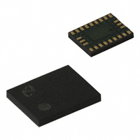
Top View Order Number LMX3305SLBX See NS Package Number SLB24A
www.national.com 101361 Version 3 Revision 5
2 Print Date/Time: 2009/04/28 20:23:25
�LMX3305
Pin Descriptions
Pin No. 1 2 3 4 Pin Name RF_CPo RF_GND RF_FIN RF_VCC I/O O PWR I PWR Description Charge pump output for RF PLL. For connection to a loop filter for driving the input of an external VCO. RF PLL ground. RF prescaler input. Small signal input from the RF Cellular or PCS VCO. RF PLL power supply voltage. Input may range from 2.7V to 3.6V. Bypass capacitors should be placed as close as possible to this pin and be connected directly to the ground plane. Tx VCC = Rx VCC = RF VCC. Multiplexed output of the RF, Rx, and Tx PLL's analog or digital lock detects. The outputs from the R, N and Fastlock counters can also be selected for test purposes. Refer to Section 2.3.4 for more detail. No Connect. I I I I I I I O RF PLL enable pin. A LOW on RF En powers down the RF PLL and TRI-STATE®s the RF PLL charge pump. Rx PLL enable pin. A LOW on Rx En powers down the Rx PLL and TRI-STATEs the Rx PLL charge pump. Tx PLL enable pin. A LOW on Tx En powers down the Tx PLL and TRI-STATEs the Tx PLL charge pump. High impedance CMOS clock input. Data for the various counters is clocked on the rising edge into the CMOS input. Binary serial data input. Data entered MSB first. High impedance CMOS input. When LE goes LOW, data is transferred into the shift registers. When LE goes HIGH, data is transferred from the internal registers into the appropriate latches. Tx prescaler input. Small signal input from the Tx VCO. Charge pump output for Tx PLL. For connection to a loop filter for driving the input of an external VCO. Tx PLL ground. PWR Tx PLL power supply voltage input. Input may range from 2.7V to 3.6V. Bypass capacitors should be placed as close as possible to this pin and be connected directly to the ground plane. Tx VCC = Rx VCC = RF VCC. PLL reference input which has a VCC/2 input threshold and can be driven from an external CMOS or TLL logic gate. The R counter is clocked on the falling edge of the OSCIN signal. Rx PLL power supply voltage. Input ranges from 2.7V to 3.6V. Bypass capacitors should be placed as close as possible to this pin and be connected directly to the ground plane. Tx VCC = Rx VCC = RF VCC. Rx PLL ground. Charge pump output for Rx PLL. For connection to a loop filter for driving the input of an external VCO. Rx prescaler input. Small signal input from the Rx VCO. An open drain NMOS output which can be use for bandswitching or Fastlocking the RF PLL. (During Fastlock mode a second loop filter damping resistor can be switched in parallel with the first to ground.) Refer to Section 2.5.3 for more detail. An open drain NMOS output which can be use for bandswitching or Fastlocking the RF PLL. (During Fastlock mode a second loop filter damping resistor can be switched in parallel with the first to ground.) Refer to Section 2.5.3 for more detail. RF PLL charge pump power supply. An internal voltage doubler can be enabled in 3V applications to allow the RF charge pump to operate over a wider tuning range.
5
Lock_Det
O
6 7 8 9 10 11 12 13 14 15 16
N/C RF_En Rx_En Tx_En Clock Data LE Tx_FIN Tx_CPo Tx_GND Tx_VCC
17 18
OSCIN Rx_VCC
I PWR
19 20 21 22
Rx_GND Rx_CPo Rx_FIN RF_Sw1
PWR O I O
23
RF_Sw2
O
24
VP
O
3 101361 Version 3 Revision 5 Print Date/Time: 2009/04/28 20:23:25
www.national.com
�LMX3305
Absolute Maximum Ratings (Notes 1, 2)
Power Supply Voltage (PLL VCC) (Note 3) Supply Voltage (VP) Voltage on any Pin with GND = 0V (VI) Storage Temperature Range (TS) −0.3V to +6.5V −0.3V to +6.5V −0.3V to VCC +0.3V −65°C to +150°C
Lead Temp. (solder, 4 sec.) (TL) ESD - Whole Body Model (Note 2)
+240°C 2 kV
Recommended Operating Conditions (Note 1)
Power Supply Voltage (PLL VCC) (Note 3) Supply Voltage (VP) (Note 3) Operating Temperature (TA) 2.7V to 3.6V PLL VCC to 5.5V −30°C to +85°C
Electrical Characteristics
(VCC = VP = 3V, −30°C < TA < 85°C except as specified) Symbol GENERAL ICC ICC-PWDN fIN Power Supply Current Power Down Current PCS Operating Frequency Cellular Operating Frequency IF Operating Frequency (Rx, Tx) fOSC fφ PfIN PfOSC RF PN IF PN Oscillator Frequency Phase Detector Frequency PCS/Cellular/IF Input Sensitivity Oscillator Sensitivity RF Phase Noise IF Phase Noise Fractional Spur @ 10 kHz Fractional Spur Harmonic Tsw Switching Speed 1 kHz Loop Filter, 60 MHz Jump to Within 1 kHz VDo = VP/2 (Note 5) VDo = VP/2 (Note 5) VDo = VCC/2 (Note 5) VDo = VCC/2 (Note 5) (Note 6) 3 8 5 0.8 VCC 0.2 VCC 0.4 −1.0 −1.0 1.0 1.0 100 1 kHz Loop Filter (Note 4) FOUT = 1 GHz 2.7V ≤ VCC ≤ 3.6V −15 0.5 −70 −70 −50 Attenuate 6 dB/OCT after 10 kHz 4.0 1200 800 45 19.68 RF = On, Rx = On, Tx = On 2.7V ≤ VCC ≤ 3.6V 9.0 10 15 75 2300 1400 600 25 10 +0 VCC MHz MHz dBm VPP dBc/Hz dBc dBc ms MHz mA µA Parameter Conditions Value Min Typ Max Unit
CHARGE PUMP RF IDo Source RF IDo Sink IF IDo Source IF IDo Sink IDo-TRI IDo Sink vs IDo Source IDo vs VDo IDo vs TA VIH VIL VOL IIH IIL IIH RF Charge Pump Source Current RF Charge Pump Sink Current IF Charge Pump Source Current IF Charge Pump Sink Current Charge Pump TRI-STATE Current −22 −22 80 −80 INOM INOM 100 −100 22 22 120 −120 1000 10 15 10 % % µA µA pA % % % V V V µA µA µA
Charge Pump Sink vs Source Mismatch TA = 25°C (Note 7) Charge Pump Current vs Voltage TA = 25°C (Note 6)
Charge Pump Current vs Temperature (Note 7) High-Level Input Voltage Low-Level Input Voltage Low-Level Output Voltage High-Level Input Current Low-Level Input Current OSCIN High-Level Input Current VCC = 2.7V to 3.6V VCC = 2.7V to 3.6V IOL = 2 mA VIH = VCC = 3.6V VIL = 0V, VCC = 3.6V VIH = VCC = 3.6V
DIGITAL INPUTS AND OUTPUTS
www.national.com 101361 Version 3 Revision 5
4 Print Date/Time: 2009/04/28 20:23:25
�LMX3305
Symbol IIL tCS tCH tCWH TCWL tENSL tENW
Parameter OSCIN Low-Level Input Current Data to Clock Setup Time Data to Clock Hold Time Clock Pulse Width High Clock Pulse Width Low Clock to Load_En Setup Time Load_En Pulse Width
Conditions VIL = 0V, VCC = 3.6V
Value Min −100 50 10 50 50 50 50 Typ Max
Unit µA ns ns ns ns ns ns
Note 1: Absolute Maximum Ratings indicate limits beyond which damage to the device may occur. Recommended Operating Conditions indicate conditions for which the device is intended to be functional, but do not guarantee specific performance limits. For guaranteed specifications and test conditions, see the Electrical Characteristics. Note 2: This device is a high performance RF integrated circuit and is ESD sensitive. Handling and assembly of this device should be done on ESD protected workstations. Note 3: PLL VCC represents RF VCC, Tx VCC and Rx VCC collectively. Note 4: Guaranteed by design. Not tested in production. Note 5: INOM = 100 µA, 400 µA, 700 µA or 900 µA for RF charge pump. Note 6: For RF charge pump, 0.5 ≤ VDo ≤ VP - 0.5; for IF charge pump, 0.5 ≤ VDo ≤ VCC - 0.5. Note 7: For RF charge pump, VDo = VP/2, for IF charge pump, VDo = VCC/2.
5 101361 Version 3 Revision 5 Print Date/Time: 2009/04/28 20:23:25
www.national.com
�LMX3305
Charge Pump Current Specification Definitions
10136104
I1 = CP sink current at VDo = VP − ΔV I2 = CP sink current at VDo = VP/2 I3 = CP sink current at VDo = ΔV I4 = CP source current at VDo = VP − ΔV I5 = CP source current at VDo = VP/2 I6 = CP source current at VDo = ΔV ΔV = Voltage offset from positive and negative rails. Dependent on VCO tuning range relative to VCC and ground. Typical values are between 0.5V and 1.0V. 1. IDo vs VDo = Charge Pump Output Current magnitude variation vs Voltage = [½ * {|I1| − |I3|}] / [½ * {|I1| + |I3|}] * 100% and [½ * {|I4| − |I6|}] / [½ * {|I4| + |I6|}] * 100% 2. IDo-sink vs IDo-source = Charge Pump Output Current Sink vs Source Mismatch = [|I2| − |I5|] / [½ * {|I2| + |I5|}] * 100% 3. IDo vs TA = Charge Pump Output Current magnitude variation vs Temperature = [|I2 @ temp| − |I2 @ 25°C|] / |I2 @ 25°C| * 100% and [|I5 @ temp| − |I5 @ 25°C|] / |I5 @ 25°C| * 100%
www.national.com 101361 Version 3 Revision 5
6 Print Date/Time: 2009/04/28 20:23:25
�LMX3305
1.0 Functional Description
The LMX3305 phase-lock-loop (PLL) system configuration consists of a high-stability crystal reference oscillator, three frequency synthesizers, three voltage controlled oscillators (VCO), and three passive loop filters. Each of the frequency synthesizers includes a phase detector, a current mode charge pump, as well as programmable reference [R] and feedback [N] frequency dividers. The VCO frequency is established by dividing the crystal reference signal down via the R-counter to obtain a comparison reference frequency. This reference signal (fR) is then presented to the input of a phase/ frequency detector and compared with the feedback signal (fN), which is obtained by dividing the VCO frequency down by way of the N-counter, and fractional circuitry. The phase/ frequency detector's current source output pumps charge into the loop filter, which then converts the charge into the VCO's control voltage. The function of phase/frequency comparator is to adjust the voltage presented to the VCO until the feedback signal frequency and phase match that of the reference signal. When the RF PLL is in a “Phase-Locked” condition, the RF VCO frequency will be (N + F) times that of the comparison frequency, where N is the integer divide ratio, and F is the fractional component. The fractional synthesis allows the phase detector frequency to be increased while maintaining the same frequency step size for channel selection. The divider ratio N is thereby reduced giving a lower phase noise referred to the phase detector input, and the comparison frequency is increased allowing faster switching time. 1.1 REFERENCE OSCILLATOR INPUTS The reference oscillator frequency for the RF and IF PLLs are provided from the external references through the OSCIN pin. OSCIN input can operate up to 25 MHz with input sensitivity of 0.5 VPP minimum and it drives RF, Rx and Tx R-counters. OSCIN input has a VCC/2 input threshold that can be driven from an external CMOS or TTL logic gate. Typically, the OSCIN is connected to the output of a crystal oscillator. 1.2 REFERENCE DIVIDERS (R-COUNTERS) The RF, Rx and Tx R-counters are clocked through the oscillator block. The maximum frequency is 25 MHz. All RF, Rx and Tx R-counters are CMOS design. The RF R-counter is 8bit in length with programmable divider ratio from 2 to 255. The Rx and Tx R-counters are 10-bit in length with programmable divider ratio from 2 to 1023. 1.3 PRESCALERS The LMX3305 has a 16/17/20/21 quadruple modulus prescaler for the PCS application and a 8/9/12/13 quadruple modulus prescaler for the cellular application. The Rx and Tx prescalers are dual modulus with 8/9 modulus ratio. Both RF/ IF prescalers' outputs drive the subsequent CMOS flip-flop chain comprising the programmable N feedback counters. 1.4 FEEDBACK DIVIDERS (N-COUNTERS) The RF, Rx and Tx N-counters are clocked by the output of RF, Rx and Tx prescalers respectively. The RF N-counter is composed of two parts: the 15 MSB bits comprise the integer portion and the 4 LSB bits comprise the fractional portion. The RF fractional N divider is fully programmable from 80 to 32767 over the frequency range from 1200 MHz-2300 MHz for PCS application and 40 to 16383 over the frequency range from 800 MHz-1400 MHz for cellular application. The 4-bit fractional portion of the RF counter represents the fraction's numerator. The fraction's denominator base is determined by the four FRAC_D register bits.
The Rx and Tx N-counters are each a 13-bit integer divisor, fully programmable from 56 to 8,191 over the frequency range from 45 MHz–600 MHz. The Rx and Tx N-counters do not include fractional compensation. 1.5 FRACTIONAL COMPENSATION The fractional compensation circuitry of the LMX3305 RF divider allows the user to adjust the VCO tuning resolution in 1/2 through 1/16th increments of the phase detector comparison frequency. A 4-bit denominator register (FRAC_D) selects the fractional modulo base. The integer averaging is accomplished by using a 4-bit accumulator. A variable phase delay stage compensates for the accumulated integer phase error, minimizes the charge pump duty cycle and reduces the spurious levels. This technique eliminates the need for compensation current injection into the loop filter. An overflow signal generated by the accumulator is equivalent to one full RF VCO cycle, and results in a pulse swallow. 1.6 PHASE/FREQUENCY DETECTORS The RF and IF phase/frequency detectors are driven from their respective N- and R-counter outputs. The maximum frequency at the phase detector inputs is 10 MHz unless limited by the minimum continuous divide ratio of the multi-modulus prescaler. The phase detector output controls the charge pump. The polarity of the pump-up or pump-down control is programmed using RF_PD_POL, Rx_PD_POL, or Tx_PD_POL depending on whether RF or IF VCO characteristics are positive or negative. The phase detector also receives a feedback signal from the charge pump in order to eliminate dead zones. 1.7 CHARGE PUMPS The phase detector's current source output pumps charge into an external loop filter, which then converts it into the VCO's control voltage. The charge pump steers the charge pump output CPo to VCC (pump-up) or Ground (pump-down). When locked, CPo is primarily in a TRI-STATE mode with small corrections. The IF charge pump output current magnitudes are nominally 100 µA. The RF charge pump output currents can be programmed by the RF_Icpo bits at 100 µA, 400 µA, 700 µA, or 900 µA. 1.8 VOLTAGE DOUBLER (VP) The VP pin is normally driven from an external power supply over a range of VCC to 5.5V to provide current for the RF charge pump circuit. An internal voltage doubler circuit connected between the VCC and VP supply pins alternately allows VCC = 3V (±10%) users to run the RF charge pump circuit at close to twice the VCC power supply voltage. The voltage doubler mode is enabled by setting the V2X bit to a HIGH level. The voltage doubler's charge pump driver originates from the oscillator input. The device will not totally powerdown until the V2X bit is programmed LOW. The average delivery current of the doubler is less than the instantaneous current demand of the RF charge pump when active and is thus not capable of sustaining a continuous out of lock condition. A large external capacitor connected to VP (=0.1 µF) is needed to control power supply droop when changing frequencies. 1.9 MICROWIRE INTERFACE The programmable register set is accessed through the microwire serial interface. The interface is comprised of three signal pins: Clock, Data, and LE. After the LE goes LOW, serial data is clocked into the 32-bit shift register upon the rising edge of Clock MSB first. The last three data bits shifted into the shift register select one of five addresses. When LE goes
7 101361 Version 3 Revision 5 Print Date/Time: 2009/04/28 20:23:25
www.national.com
�LMX3305
HIGH, data is transferred from the shift registers into one of the four register bank latches. Selecting the address presets the data in the four register banks. The synthesizer can be programmed even in the power down (or not enabled) state. 1.10 LOCK DETECT OUTPUTS The open-drain Lock Detect is available in the LMX3305 to provide a digital or analog lock detect indication for the sum of the active PLLs. In the digital lock detect mode, an internal digital filter produces a logic level HIGH at the lock detect output when the error between the phase detector inputs is less than 15 ns for five consecutive comparison cycles. The lock detect output is LOW when the error between the phase detector inputs is more than 30 ns for one comparison cycle. In the analog lock detect mode, the lock detect pin becomes active low whenever any of the active PLLs are charge pumping. The Lock_Det pin can also be programmed to provide the outputs of the R, N or fastlock timeout counters. 1.11 POWER CONTROL Each PLL is individually power controlled by the microwire power down bits Rx_PWDN, Tx_PWDN and RF_PWDN. Alternatively, the PLLs can also be power controlled by the Tx_En, Rx_En, and RF_En pins. The enable pins override the power down bits except for the V2X bit. When the respective PLL's enable pin is high, the power down bits determine the state of power control. Activation of any PLL power down modes result in the disabling of the respective N counter and de-biasing of its respective fIN input (to a high impedance state). The R counter functionality also becomes disabled when the power down bit is activated. The reference oscillator block powers down and the OSCIN pin reverts to a high impedance state when all of the enable pins are LOW or all of the power down bits are programmed HIGH, unless V2X bit is HIGH. Power down forces the respective charge pump and phase comparator logic to a TRI-STATE condition. A power down counter reset function resets both N and R counters of the respective PLL. Upon powering up the N counter resumes counting in “close” alignment with the R counter (the maximum error is one prescaler cycle). The microwire control register remains active and capable of loading and latching in data during all of the power down modes.
2.0 Programming Description
www.national.com 101361 Version 3 Revision 5
8 Print Date/Time: 2009/04/28 20:23:25
�2.1 MICROWIRE SERIAL BUS INTERFACE The LMX3305 uses Clock, Data, and LE signals to accomplish all data transactions. Data is latched into the 32-bit shift register on the rising edge of Clock, MSB first. The last three bits loaded are the address bits that determine which of the four Data register banks the shift register data will be transferred to when LE goes HIGH. Most Significant Bit SHIFT REGISTER BIT LOCATION Least Significant Bit 25 Data Field 24 23 22 21 20 19 18 17 16 15 14 13 12 11 10 9 8 7 6 5 4 3 2 1 0 Address Field 0 X Rx_RST 0 0 0 0 1
31
30
29
28
27
26
P
All Register bits Preset (Upon LE latching address )
IF_R
Tx_RST
Tx_R_CNTR [9:0]
LD [3:0]
Rx_R_CNTR [9:0]
IF_R9
IF_R8
IF_R7
IF_R6
IF_R5
IF_R4
IF_R3
IF_R2 Rx_PD_POL
IF_R28
IF_R27
IF_R26
IF_R25
IF_R24
IF_R23
IF_R22
IF_R21
IF_R20
IF_R19
IF_R18 Tx_PD_POL
IF_R17
IF_R16
IF_R15
IF_R14
IF_R13
IF_R12
IF_R11
IF_R10
IF_R0 X Rx_NA_CNTR [2:0] 0
1
0
IF_N
Tx_PWDN
IF_N9
IF_N8
IF_N7
IF_N6
IF_N5
IF_N4
IF_N3
IF_N1 Rx_PWDN IF_R1
IF_N28
IF_N27
IF_N26
IF_N25
IF_N24
IF_N23
IF_N22
IF_N21
IF_N20
IF_N19
IF_N18
IF_N17
IF_N16
IF_N15
IF_N14
IF_N13
IF_N12
IF_N11
IF_N10
IF_N0 0 RF_Icpo RF_RST V2X FRAC_CAL [4:0]
FSTM2
FSTM1
FSTSW2
RF_R
FSTSW1
RF_R9
RF_R8
RF_R7
RF_R6
RF_R2 RF_PD_POL IF_N2
RF_R1
RF_R28
RF_R27
RF_R26
RF_R25
RF_R24
RF_R23
RF_R22
RF_R21
RF_R20
RF_R19
RF_R18
RF_R17
RF_R16
RF_R15
RF_R14
RF_R13
RF_R12
RF_R11
RF_N_CNTR [14:0] RF_N22 RF_N21 RF_N20 RF_N19 RF_N18 RF_N17 RF_N16 RF_N15 RF_N14 RF_N13
FRAC_N [3:0] RF_N9 RF_N12 RF_N11 RF_N10
FRAC_D [3:0] RF_N8 RF_N7 RF_N6
RF_N
RF_N5
Fbps RF_R5
RF_N4
PCS RF_R4
RF_N3 RF_PWDN RF_R3
RF_N2
RF_N1
RF_N28
RF_N27
RF_N26
RF_N25
RF_N24
Note: X denotes don't care bits.
RF_N23
RF_N0
LMX3305
Print Date/Time: 2009/04/28 20:23:25
RF_R10
Test [2:0]
RF_R0
101361 Version 3 Revision 5
Tx_NB_CNTR [9:0]
Tx_NA_ CNTR [2:0] Rx_NB_CNTR [9:0]
9
1
1
RF_R_CNTR [7:0]
FSTL_CNTR [6:0]
1
0
0
www.national.com
�LMX3305
P
Tx_PD_ POL
Tx_RST
Rx_PD_ POL
IF_R
0 IF_R9 IF_R8 IF_R7 IF_R6 IF_R5 IF_R4 IF_R3 IF_R20 IF_R19 IF_R18 IF_R17 IF_R16 IF_R15 IF_R14 IF_R13 IF_R12 IF_R11 IF_R10
0
0
0
0
1
0
0
0
0
1
0
0
0
0
0
0
0
1
0
1
0
0
1
0
0
1 IF_R2
Rx_RST
IF_R1
IF_R28
IF_R27
IF_R26
IF_R25
IF_R24
IF_R23
IF_R22
IF_R21
IF_R0
Tx_PWDN
IF_N
IF_N9
IF_N8
IF_N7
IF_N6
IF_N5
IF_N4
IF_N28
IF_N27
IF_N26
IF_N25
IF_N24
IF_N23
IF_N22
IF_N21
IF_N20
IF_N19
IF_N18
IF_N17
IF_N16
IF_N15
IF_N14
IF_N13
IF_N12
IF_N11
IF_N10
IF_N3
FSTM2
FSTM1
FSTSW2
FSTSW1
RF_Icpo
RF_R
0 RF_R20 RF_R19 RF_R18 RF_R17 RF_R16 RF_R15 RF_R14 RF_R13 RF_R12 RF_R11
0
1
0
1
0
0
1
0
1
1
1
1
0
0
1
1
0
0 RF_R10
0 RF_R9
0 RF_R8
0 RF_R7
0 RF_R6
0 RF_R5
1 RF_R4
1 RF_R3
RF_PD_POL IF_N2
1 RF_R2
RF_RST IF_N1
RF_R_CNTR [7:0]
FSTL_CNTR [6:0]
FRAC_CAL [4:0]
0 RF_R1
RF_R28
RF_R27
RF_R26
RF_R25
RF_R24
RF_R23
RF_R22
Fbps
PCS
RF_N
0 RF_N20 RF_N19 RF_N18 RF_N17 RF_N16 RF_N15
0
0
1
1
1
1
1
0
1
1
0
1
1
0 RF_N14
0 RF_N13
1 RF_N12
1 RF_N11
0 RF_N10
0 RF_N9
0 RF_N8
0 RF_N7
0 RF_N6
0 RF_N5
0 RF_N4
RF_PWDN
RF_N3
RF_N2
RF_N1
RF_N28
RF_N27
RF_N26
RF_N25
RF_N24
RF_N23
RF_N22
These preset bit states provide the following local oscillator conditions for an OSCIN frequency of 19.68 MHz: Rx PLL: Rmod = 164 PLL: Rmod = 16 Nmod = 212 phase detect freq = 1.23 MHz Fvco = 260.76 MHz RF PLL: Rmod = 41, T.O count = 480
RF_N21
Nmod = 1423 phase detect freq = 120 kHz Fvco = 170.76 MHz Tx Nmod = 2014 6 / 16 phase detect freq = 480 kHz Fvco = 966.90 MHz
RF_N0
Print Date/Time: 2009/04/28 20:23:25
RF_R21
Test [2:0] FRAC_N [3:0] FRAC_D [3:0]
RF_R0
V2X IF_N0
101361 Version 3 Revision 5
0
0
0
0
0
1
1
0
1
0
1
0
0
0
0
0
1
0
1
1
0
0
0
1
1
1
1
Rx_PWDN
www.national.com
2.2 P REGISTER P register has the special function of programming all of the registers to a preset known set state shown below. Note that this does not prevent the other four address registers from being programmed after this. Most Significant Bit SHIFT REGISTER BIT LOCATION Least Significant Bit 23 Data Field All Register bits Preset LD [3:0] Rx_R_CNTR [9:0] (Upon LE latching address ) X 22 21 20 19 18 17 16 15 14 13 12 11 10 9 8 7 6 5 4 3 2 0 0 1 0 0 0 Address Field 0 1
31 30 29 28 27 26 25 24
Tx_R_CNTR [9:0]
0
0
X Rx_NA_CNTR [2:0]
0
1
0
Tx_NB_CNTR [9:0]
Tx_NA_ CNTR [2:0] Rx_NB_CNTR [9:0]
0
0
10
0
1
1
0
1
0
0
RF_N_CNTR [14:0]
0
0
0
0
�2.3 IF_R REGISTER If the ADDRESS [2:0] field is set to 001, data is transferred from the 32-bit shift register into the IF_R register when LE signal goes high. The IF_R register sets the Rx PLL's 10-bit R counter divide ratio, the Tx PLL's 10-bit R counter divide ratio and various programmable bits. The divide ratio for both Rx and Tx R counters are from 2 to 1023. Most Significant Bit SHIFT REGISTER BIT LOCATION Least Significant Bit 22 Data Field X 21 20 19 18 17 16 15 14 13 12 11 10 9 8 7 6 5 4 3 2 1 0
31 30 29 28 27 2 25 2 23 6 4 0 0
Address Field 1
Tx_RST
IF_R
IF_R9
IF_R8
IF_R7
IF_R6
IF_R5
IF_R4
IF_R3
IF_R2 Rx_PD_POL IF_R1
Rx_RST IF_R0
Tx_R_CNTR [9:0]
LD [3:0]
Rx_R_CNTR [9:0]
IF_R28
IF_R27
IF_R26
IF_R25
IF_R24
IF_R23
IF_R22
IF_R21 IF_R20
IF_R19
IF_R18 Tx_PD_POL IF_R17
IF_R16
IF_R15
IF_R14
IF_R13
IF_R12
IF_R11
LMX3305
101361 Version 3 Revision 5
Note: X denotes don't care bit.
IF_R10
11
Print Date/Time: 2009/04/28 20:23:25
www.national.com
�LMX3305
2.3.1 10-Bit IF Programming Reference Divider Ratio (Tx R Counter, Rx R Counter) Divide Ratio 2 3 • 1023 0 0 • 1 0 0 • 1 Tx_R_CNTR [9:0] or Rx_R_CNTR [9:0] 0 0 • 1 0 0 • 1 0 0 • 1 0 0 • 1 0 0 • 1 0 0 • 1 1 1 • 1 0 1 • 1
Note: Divide ratio for both Tx and Rx R counters are from 2 to 1023.
2.3.2 Tx_PD_POL (IF_R[18]) This bit sets the polarity of the Tx phase detector. It is set to one when Tx VCO characteristics are positive. When Tx VCO frequency decreases with increasing control voltage, Tx_PD_POL should be set to zero. 2.3.3 Tx_RST (IF_R[17]) This bit will reset the Tx R and N counters when it is set to one. For normal operation, Tx_RST should be set to zero.
2.3.4 LD (IF_R[16]-[13]) The LD pin is a multiplexed output. When in lock detect mode, LD does ANDing function on the active PLLs. The RF fractional test mode is only intended for factory testing.
Lock Detect Output Truth Table LD [3:0] 0 0 1 1 1 1 1 1 1 1 0 0 0 0 0 0 1 1 1 1 0 0 0 0 1 1 0 0 1 1 0 1 0 1 0 1 0 1 0 1 LD Pin Function Digital Lock Detect Analog Lock Detect Rx R Counter Rx N Counter Tx R Counter Tx N Counter RF R Counter RF N Counter RF Fastlock Timeout Counter RF Fractional Test Mode Output Format Open Drain Open Drain CMOS CMOS CMOS CMOS CMOS CMOS CMOS Analog
Lock Detect Digital Filter The Lock Detect Digital Filter compares the difference between the phase of the inputs of the phase detector to a RC generated delay of approximately 15 ns. To enter the locked state (Lock Det = HIGH) the phase error must be less than the 15 ns RC delay for five consecutive reference cycles.
Once in lock (Lock Det = HIGH), the RC delay is changed to approximately 30 ns. To exit the locked state (Lock Det = LOW), the phase error must become greater than the 30 ns RC delay. When the PLL is in the powerdown mode, Lock Det is forced HIGH. A flow chart of the digital filter is shown below.
www.national.com 101361 Version 3 Revision 5
12 Print Date/Time: 2009/04/28 20:23:25
�LMX3305
10136105
13 101361 Version 3 Revision 5 Print Date/Time: 2009/04/28 20:23:25
www.national.com
�LMX3305
Typical Lock Detect Timing
10136106
2.3.5 Rx_PD_POL (IF_R[2]) This bit sets the polarity of the Rx phase detector. It is set to one when Rx VCO characteristics are positive. When Rx VCO frequency decreases with increasing control voltage, Rx_PD_POL should set to zero.
2.3.6 Rx_RST (IF_R[1]) This bit will reset the Rx R and N counters when it is set to one. For normal operation, Rx_RST should be set to zero.
www.national.com 101361 Version 3 Revision 5
14 Print Date/Time: 2009/04/28 20:23:25
�2.4 IF_N REGISTER If the ADDRESS [2:0] field is set to 010, data is transferred from the 32-bit shift register into the IF_N register when LE signal goes high. The IF_N register sets the Rx PLL's 13-bit N counter divide ratio, the Tx PLL's 13-bit N counter divide ratio and various programmable bits. Both N counters consist of the 3-bit swallow counter (A counter) and the 10-bit programmable counter (B counter). N divider continuous integer divide ratio is from 56 to 8191. Most Significant Bit SHIFT REGISTER BIT LOCATION Least Significant Bit 25 Data Field X Rx_PWDN Tx_NA_ CNTR [2:0] Rx_NB_CNTR [9:0] IF_N14 IF_N13 IF_N12 IF_N11 IF_N10 IF_N21 IF_N20 IF_N19 IF_N18 IF_N17 IF_N16 IF_N9 IF_N8 IF_N7 IF_N6 IF_N5 IF_N4 IF_N3 IF_N2 IF_N1 Rx_NA_ CNTR [2:0] 0 24 23 22 21 20 19 18 17 16 15 14 13 12 11 10 9 8 7 6 5 4 3 2 1 1 0 0 Address Field
31
30
29
28
27
26
Tx_NB_CNTR [9:0] IF_N22
IF_N
IF_N28
IF_N27
IF_N26
IF_N25
IF_N24
IF_N23
IF_N15 Tx_PWDN
LMX3305
101361 Version 3 Revision 5
Note: X denotes don't care bit.
IF_N0
15
Print Date/Time: 2009/04/28 20:23:25
www.national.com
�LMX3305
2.4.1 3-Bit IF Swallow Counter Divide Ratio (Tx A Counter, Rx A Counter) Divide Ratio 0 1 • 7
Divide ratio is from 0 to 7
Tx_NA_CNTR [2:0] or Rx_NA_CNTR [2:0] 0 0 • 1 0 0 • 1 0 1 • 1
Tx_NB_CNTR ≥ Tx_NA_CNTR and Rx_NB_CNTR ≥ Rx_NA_CNTR
2.4.2 10-Bit IF Programmable Counter Divide Ratio (Tx B Counter, Rx B Counter) Divide Ratio 3 4 • 1023 0 0 • 1 0 0 • 1 0 0 • 1 Tx_NB_CNTR [9:0] or Rx_NB_CNTR [9:0] 0 0 • 1 0 0 • 1 0 0 • 1 0 0 • 1 0 1 • 1 1 0 • 1 1 0 • 1
Divide ratio is from 3 to 1023 (Divide ratios less than 3 are prohibited)
Tx_NB_CNTR ≥ Tx_NA_CNTR and Rx_NB_CNTR ≥ Rx_NA_CNTR N = PB + A B = N div P A = N mod P
2.4.3 Tx_PWDN (IF_N[15]) This bit will asynchronously powerdown the Tx PLL when set to one. For normal operation, it should be set to zero.
2.4.4 Rx_PWDN (IF_N[1]) This bit will asynchronously powerdown the Rx PLL when set to one. For normal operation, it should be set to zero.
www.national.com 101361 Version 3 Revision 5
16 Print Date/Time: 2009/04/28 20:23:25
�2.5 RF_R REGISTER If the ADDRESS [2:0] field is set to 011, data is transferred from the 32-bit shift register into the RF_R register when LE signal goes high. The RF_R register sets the RF PLL's 8-bit R counter divide ratio and various programmable bits. The divide ratio for RF R counter is from 2 to 255. Most Significant Bit SHIFT REGISTER BIT LOCATION Least Significant Bit 25 Data Field 0 V2X 24 23 22 21 20 19 18 17 16 15 14 13 12 11 10 9 8 7 6 5 4 3 2 1 1 0 1 Address Field
31
30
29
28
27
26
FSTM2
FSTM1
RF_Icpo
FSTSW2
FSTSW1
RF_R
RF_R28
RF_R27
RF_R26
RF_R25
RF_R24
RF_R23
RF_R22
RF_R21
RF_R20
RF_R19
RF_R18
RF_R17
RF_R16
RF_R15
RF_R14
RF_R13
RF_R12
RF_R11
RF_R10
RF_R9
RF_R8
RF_R7
RF_R6
RF_R5
RF_R4
RF_R3
RF_R2
RF_PD_POL RF_R1 RF_RST
RF_R_CNTR [7:0]
FSTL_CNTR [6:0]
FRAC_CAL [4:0]
RF_R0
LMX3305
101361 Version 3 Revision 5
17
Print Date/Time: 2009/04/28 20:23:25
www.national.com
�LMX3305
2.5.1 8-Bit RF Programming Reference Divider Ratio (RF R Counter) Divide Ratio 2 3 • 255 0 0 • 1 0 0 • 1 0 0 • 1 RF_R_CNTR [7:0] 0 0 • 1 0 0 • 1 0 0 • 1 1 1 • 1 0 1 • 1
Divide ratio for RF R counter is from 2 to 255.
2.5.2 FSTL_CNTR (RF_R[20]-[14]) The Fastlock Timeout Counter is a 10 bit counter wherein only the seven MSB bits are programmable. (The number of phase Phase Detect Cycles 24 32 • 1008 1016 0 0 • 1 1 0 0 • 1 1 0 0 • 1 1
detector cycles the fastlock mode remains in HIGH gain is the binary FSTL_CNTR value loaded multiplied by eight.)
FSTL_CNTR [6:0] 0 0 • 1 1 0 1 • 1 1 1 0 • 1 1 1 0 • 0 1
2.5.3 FSTM (RF_R[13]-[12]) and FSTSW (RF_R[11]-[10]) Fastlock enables the designer to achieve both fast frequency transitions and good phase noise performance by dynamically changing the PLL loop bandwidth. The Fastlock modes allow wide band PLL fast locking with seamless transition to a low phase noise narrow band PLL. Consistent gain and phase margins are maintained by simultaneously changing charge pump current magnitude and loop filter damping resistor. In the LMX3305, the RF fastlock can achieve substantial improvement in lock time by increasing the charge pump current by 4X, 7X or 9X, which causes a 2X, 2.6X or 3X increase in the loop bandwidth respectively. The damping resistors are connected to FSTSW pins. RF_R[12] FSTM1 0 0 1 RF_R[13] FSTM2 0 0 1 RF_R[10] FSTSW1 0 1 x RF_R[11] FSTSW2 0 1 x
When bit FSTM2 and/or FSTM1 is set HIGH, the RF fastlock is enabled. As a new frequency is loaded, RF_Sw2 pin and/ or RF_Sw1 pin goes to a LOW state to switch in the damping resistors, the RF CPo is set to a higher gain, and fastlock timeout counter starts counting. Once the timeout counter finishes counting, the PLL returns to its normal operation (the Icpo gain is forced to 100 µA irrespective of RF_Icpo bits). When bit FSTM2 and/or FSTM1 is set LOW, pins RF_Sw2 and/or RF_Sw1 can be toggled HIGH or LOW to drive other devices. RF_Sw2 and/or RF_Sw1 can also be set LOW to switch in different damping resistors to change the loop filter performance. FSTSW bits control the output states of the RF_Sw2 and RF_Sw1 pins. RF_Sw1 Output Function
RF_Sw1 pin reflects RF_SwBit “0” logic state RF_Sw1 pin reflects RF_SwBit “1” logic state RF_Sw1 pin LOW while T.O. counter is active RF_Sw2 Output Function RF_Sw2 pin reflects RF_SwBit “0” logic state RF_Sw2 pin reflects RF_SwBit “1” logic state RF_Sw2 pin LOW while T.O. counter is active tional spur. Improvements can be made by selecting the bits to be one greater or less than the denominator value. For example, in the 1/16 fractional mode, these four bits can be programmed to 15 or 17. In normal operation, these bits should be set to zero.
2.5.4 FRAC_CAL (RF_R[9]-[5]) These five bits allow the users to optimize the fractional circuitry, therefore reducing the fractional reference spurs. The MSB bit, RF_R[9], activates the other four calibration bits RF_R[8]-[5]. These four bits can be adjusted to improve frac-
www.national.com 101361 Version 3 Revision 5
18 Print Date/Time: 2009/04/28 20:23:25
�LMX3305
2.5.5 RF_Icpo (RF_R[4]-[3]) These two bits set the charge pump gain of the RF PLL. The user is able to set the charge pump gain during the acquisition phase of the fastlock mode to 4X, 7X or 9X. Charge Pump Gain 100 µA 400 µA 700 µA 900 µA 2.5.6 RF_PD_POL (RF_R[2]) This bit sets the polarity of the RF phase detector. It is set to one when RF VCO characteristics are positive. When RF VCO frequency decreases with increasing control voltage, RF_PD_POL should be set to zero. 2.5.7 RF_RST (RF_R[1]) This bit will reset the RF R and N counters when it is set to one. For normal operation, RF_RST should be set to zero. RF_R[4] 0 0 1 1 RF_R[3] 0 1 0 1 2.5.8 V2X (RF_R[0]) V2X when set high enables the voltage doubler for the RF charge pump supply.
19 101361 Version 3 Revision 5 Print Date/Time: 2009/04/28 20:23:25
www.national.com
�LMX3305
RF_N
RF_N28
RF_N27
RF_N26
RF_N25
RF_N24
RF_N23
RF_N22
RF_N21
RF_N20
RF_N19
RF_N18
RF_N17
RF_N16
RF_N15
RF_N14
RF_N13
RF_N12
RF_N11
RF_N10
RF_N9
RF_N8
RF_N7
RF_N6
RF_N5
Fbps
RF_N4
PCS
RF_N3 RF_PWDN
RF_N2
RF_N1
RF_N0
www.national.com
2.6 RF_N REGISTER If the ADDRESS [2:0] field is set to 100, data is transferred from the 32-bit shift register into the RF_N register when LE signal goes high. The RF_N register set the RF PLL's 23-bit fractional N counter and various programmable bits. The fractional N counter consists of 15 bits integer portion and 8 bits fractional portion. The integer portion consists of a 2-bit swallow counter (A word), a 2-bit programmable counter (B word) and a 11-bit programmable counter (C word). The fractional portion consists of a 4-bit numerator and a 4-bit denominator. Most Significant Bit SHIFT REGISTER BIT LOCATION Least Significant Bit 25 Data Field Test [2:0] FRAC_N [3:0] FRAC_D [3:0] 24 23 22 21 20 19 18 17 16 15 14 13 12 11 10 9 8 7 6 5 4 3 2 1 1 0 0 Address Field 0
31
30
29
28
27
26
RF_N_CNTR [14:0]
101361 Version 3 Revision 5
20
Print Date/Time: 2009/04/28 20:23:25
�LMX3305
2.6.1 RF_N_CNTR (RF_N[28]-[14]) The RF N counter value is determined by three counter values that work in conjunction with four prescalers. This quadruple modulus prescaler architecture allows lower minimum continuous divide ratios than are possible with a dual modulus prescaler architecture. For the determination of the A, B, and C counter values, the fundamental relationships are shown below.
N = PC + 4B + A C ≥ max {A,B} + 2 The A, B, and C values can be determined as follows: C = N div P B = (N - CP) div 4 A = (N - CP) mod 4
N REGISTER FOR THE CELLULAR (8/9/12/13) PRESCALER OPERATING IN FRACTIONAL MODE Divide Ratio 1-23 24-39 40 41 … 16383 0 0 . 1 0 0 . 1 0 0 . 1 0 0 . 1 C Word Some of these N values are Legal Divide Ratios, some are not 0 0 . 1 0 0 . 1 0 0 . 1 0 0 . 1 1 1 . 1 0 0 . 1 1 1 . 1 0 0 0 0 0 0 . 1 0 0 . 1 0 1 . 1 RF_N_CNTR [14:0] B Word A Word Divide Ratios Less than 24 are impossible since it is required that C ≥ 3
N REGISTER FOR THE PCS (16/17/20/21) PRESCALER OPERATING IN FRACTIONAL MODE Divide Ratio 1-47 48-79 80 81 … 32767 0 0 . 1 0 0 . 1 0 0 . 1 0 0 . 1 C Word Some of these N values are Legal Divide Ratios, some are not 0 0 . 1 0 0 . 1 0 0 . 1 0 0 . 1 1 1 . 1 0 0 . 1 1 1 . 1 0 0 0 1 0 0 . 1 0 0 . 1 0 1 . 1 RF_N_CNTR [14:0] B Word A Word Divide Ratios Less than 48 are impossible since it is required that C ≥ 3
2.6.2 FRAC_N (RF_N[13]-[10]) These four bits, the fractional accumulator modulus numerator, set the fractional numerator values in the fraction. Modulus Numerator 0 1 2 • 14 15 0 0 0 • 1 1 0 0 0 • 1 1 FRAC_N [3:0] 0 0 1 • 1 1 0 1 0 • 0 1
21 101361 Version 3 Revision 5 Print Date/Time: 2009/04/28 20:23:25
www.national.com
�LMX3305
2.6.3 FRAC_D (RF_N[9]-[6]) These four bits, the fractional accumulator modulus denominator, set the fractional denominator from 1/2 to 1/16 resolution. Modulus Denominator 1-8 9 10-14 15 16 1 • 1 0 0 • 1 0 FRAC_D [3:0] Not Allowed 0 • 1 0 1 • 1 0
MODULUS NUMERATOR (FRAC_N) AND DENOMINATOR (FRAC_D) PROGRAMMING Fractional Numerator (FRAC_N) 1 2 3 4 5 RF_N[13]- 0001 0010 0011 0100 0101 [10] 0=0000 1=0001 2=0010 * * * * (8/16) (5/15) (4/16) (3/15) * * * (10/1 (8/16) (6/15) 5) * * (12/1 (9/15) 6) * (12/1 5) Fractional Denominator, (FRAC_D) RF_N[9]-[6] 6 0110 7 0111 8 9 10 11 12 13 14 15 1000 1001 1010 1011 1100 1101 1110 1111 16 0000
Functions like an integer-N PLL as fractional component is set to 0. * * * (2/12) (2/14) (2/16) * * * (4/12) (4/14) (4/16) * * * (6/12) (6/14) (6/16) * * * (8/12) (8/14) (8/16) * (10/1 2) 1/9 2/9 1/10 2/10 1/11 2/11 1/12 2/12 1/13 2/13 1/14 2/14 1/15 2/15 1/16 2/16
3=0011
3/9
3/10
3/11
3/12
3/13
3/14
3/15
3/16
4=0100
4/9
4/10
4/11
4/12
4/13
4/14
4/15
4/16
5=0101
6=0110
7=0111
8=1000 9=1001 10=1010 11=1011 12=1100 13=1101 14=1110 15=1111
* * (10/1 (10/1 4) 6) * * (12/1 (12/1 4) 6) * (14/1 6) FRAC_D values between 1 to 8 are not allowed.
5/9
5/10
5/11
5/12
5/13
5/14
5/15
5/16
6/9
6/10
6/11
6/12
6/13
6/14
6/15
6/16
7/9
7/10
7/11
7/12
7/13
7/14
7/15
7/16
8/9
8/10 9/10
8/11 9/11 10/1 1
8/12 9/12 10/1 2 11/1 2
8/13 9/13 10/1 3 11/1 3 12/1 3
8/14 9/14 10/1 4 11/1 4 12/1 4 13/1 4
8/15 9/15 10/1 5 11/1 5 12/1 5 13/1 5 14/1 5
8/16 9/16 10/16 11/16 12/16 13/16 14/16 15/16
Remark: The *(FRAC_N / FRAC_D) denotes that the fraction number can be represented by (FRAC_N / FRAC_D) as indicated in the parenthesis. For example, 1/2 can be represented by 8/16.
www.national.com 101361 Version 3 Revision 5
22 Print Date/Time: 2009/04/28 20:23:25
�LMX3305
2.6.4 FBPS (RF_N[5]) This bit when set to one will bypass the delay line calculation used in the fractional circuitry. This will improve the phase noise while sacrificing performance on reference spurs. When the bit is set to zero, the delay line circuit is in effect to reduce reference spur. 2.6.5 PCS (RF_N[4]) This bit will determine whether the RF PLL should operate in PCS frequency range or cellular frequency range. When the
bit is set to one, the RF PLL will operate in the PCS mode and when it is set to zero, the cellular mode. 2.6.6 RF_PWDN (RF_N[3]) This bit will asynchronously powerdown the RF PLL when set to one. For normal operation, it should be set to zero. 2.6.7 Test (RF_N[2]-[0]) These bits are the internal factory testing only. They should be set to zero for normal operation.
23 101361 Version 3 Revision 5 Print Date/Time: 2009/04/28 20:23:25
www.national.com
�LMX3305
SERIAL DATA INPUT TIMING
10136107
Notes: Parenthesis data indicates programmable reference divider data. Data shifted into register on clock rising edge. Data is shifted in MSB first.
Test Conditions: The Serial Data Input Timing is tested using a symmetrical waveform around VCC/2. The test waveform has an edge rate of 0.6 V/ns with amplitudes of 1.84V @ VCC = 2.3V and 4.4V @ VCC = 5.5V.
www.national.com 101361 Version 3 Revision 5
24 Print Date/Time: 2009/04/28 20:23:25
�LMX3305
Physical Dimensions inches (millimeters) unless otherwise noted
LMX3305 Package Drawing Order Number LMX3305SLBX NS Package Number SLB24A
25 101361 Version 3 Revision 5 Print Date/Time: 2009/04/28 20:23:25
www.national.com
�LMX3305 Triple Phase Locked Loop for RF Personal Communications
Notes
For more National Semiconductor product information and proven design tools, visit the following Web sites at:
Products Amplifiers Audio Clock and Timing Data Converters Interface LVDS Power Management Switching Regulators LDOs LED Lighting Voltage Reference PowerWise® Solutions Serial Digital Interface (SDI) Temperature Sensors Wireless (PLL/VCO) www.national.com/amplifiers www.national.com/audio www.national.com/timing www.national.com/adc www.national.com/interface www.national.com/lvds www.national.com/power www.national.com/switchers www.national.com/ldo www.national.com/led www.national.com/vref www.national.com/powerwise www.national.com/sdi www.national.com/tempsensors www.national.com/wireless WEBENCH® Tools App Notes Reference Designs Samples Eval Boards Packaging Green Compliance Distributors
Design Support www.national.com/webench www.national.com/appnotes www.national.com/refdesigns www.national.com/samples www.national.com/evalboards www.national.com/packaging www.national.com/quality/green www.national.com/contacts www.national.com/quality www.national.com/feedback www.national.com/easy www.national.com/solutions www.national.com/milaero www.national.com/solarmagic www.national.com/AU
Quality and Reliability Feedback/Support Design Made Easy Solutions Mil/Aero SolarMagic™ Analog University®
THE CONTENTS OF THIS DOCUMENT ARE PROVIDED IN CONNECTION WITH NATIONAL SEMICONDUCTOR CORPORATION (“NATIONAL”) PRODUCTS. NATIONAL MAKES NO REPRESENTATIONS OR WARRANTIES WITH RESPECT TO THE ACCURACY OR COMPLETENESS OF THE CONTENTS OF THIS PUBLICATION AND RESERVES THE RIGHT TO MAKE CHANGES TO SPECIFICATIONS AND PRODUCT DESCRIPTIONS AT ANY TIME WITHOUT NOTICE. NO LICENSE, WHETHER EXPRESS, IMPLIED, ARISING BY ESTOPPEL OR OTHERWISE, TO ANY INTELLECTUAL PROPERTY RIGHTS IS GRANTED BY THIS DOCUMENT. TESTING AND OTHER QUALITY CONTROLS ARE USED TO THE EXTENT NATIONAL DEEMS NECESSARY TO SUPPORT NATIONAL’S PRODUCT WARRANTY. EXCEPT WHERE MANDATED BY GOVERNMENT REQUIREMENTS, TESTING OF ALL PARAMETERS OF EACH PRODUCT IS NOT NECESSARILY PERFORMED. NATIONAL ASSUMES NO LIABILITY FOR APPLICATIONS ASSISTANCE OR BUYER PRODUCT DESIGN. BUYERS ARE RESPONSIBLE FOR THEIR PRODUCTS AND APPLICATIONS USING NATIONAL COMPONENTS. PRIOR TO USING OR DISTRIBUTING ANY PRODUCTS THAT INCLUDE NATIONAL COMPONENTS, BUYERS SHOULD PROVIDE ADEQUATE DESIGN, TESTING AND OPERATING SAFEGUARDS. EXCEPT AS PROVIDED IN NATIONAL’S TERMS AND CONDITIONS OF SALE FOR SUCH PRODUCTS, NATIONAL ASSUMES NO LIABILITY WHATSOEVER, AND NATIONAL DISCLAIMS ANY EXPRESS OR IMPLIED WARRANTY RELATING TO THE SALE AND/OR USE OF NATIONAL PRODUCTS INCLUDING LIABILITY OR WARRANTIES RELATING TO FITNESS FOR A PARTICULAR PURPOSE, MERCHANTABILITY, OR INFRINGEMENT OF ANY PATENT, COPYRIGHT OR OTHER INTELLECTUAL PROPERTY RIGHT. LIFE SUPPORT POLICY NATIONAL’S PRODUCTS ARE NOT AUTHORIZED FOR USE AS CRITICAL COMPONENTS IN LIFE SUPPORT DEVICES OR SYSTEMS WITHOUT THE EXPRESS PRIOR WRITTEN APPROVAL OF THE CHIEF EXECUTIVE OFFICER AND GENERAL COUNSEL OF NATIONAL SEMICONDUCTOR CORPORATION. As used herein: Life support devices or systems are devices which (a) are intended for surgical implant into the body, or (b) support or sustain life and whose failure to perform when properly used in accordance with instructions for use provided in the labeling can be reasonably expected to result in a significant injury to the user. A critical component is any component in a life support device or system whose failure to perform can be reasonably expected to cause the failure of the life support device or system or to affect its safety or effectiveness. National Semiconductor and the National Semiconductor logo are registered trademarks of National Semiconductor Corporation. All other brand or product names may be trademarks or registered trademarks of their respective holders.
Copyright© 2009 National Semiconductor Corporation
For the most current product information visit us at www.national.com
National Semiconductor Americas Technical Support Center Email: support@nsc.com www.national.com Tel: 1-800-272-9959 National Semiconductor Europe Technical Support Center Email: europe.support@nsc.com National Semiconductor Asia Pacific Technical Support Center Email: ap.support@nsc.com National Semiconductor Japan Technical Support Center Email: jpn.feedback@nsc.com
101361 Version 3 Revision 5
Print Date/Time: 2009/04/28 20:23:26
�


 工商网监
湘ICP备2023018690号
工商网监
湘ICP备2023018690号
