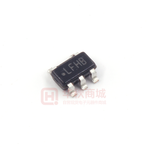
LP3992 Micropower 1.5V CMOS Voltage Regulator with Shutdown Control
December 2002
LP3992 Micropower 1.5V CMOS Voltage Regulator with Shutdown Control
General Description
The LP3992 regulator is designed to meet the requirements of portable, battery-powered systems providing an accurate output voltage, low noise, and low quiescent current. Battery life will be prolonged by the ability of the LP3992 to provide a 1.5V output from the low input voltage of 1.9V. Additionally, when switched to a shutdown mode via a logic signal at the shutdown pin, the power consumption is reduced to virtually zero. The LP3992 also features short-circuit and thermalshutdown protection. The LP3992 is designed to be stable with space saving ceramic capacitors as small as 1.0µF. The device is available in an SOT23-5 package. Performance is specified for a -40˚C to 125˚C temperature range. For output voltages other than 1.5V and alternative package options, please contact your local NSC sales office.
Key Specifications
n n n n n n 1.9 to 5.2V input range Accurate 1.5V ± 0.09V output voltage Less than 1.5µA quiescent current in shutdown Stable with a 1µF output capacitor Guaranteed 30mA output current Low output voltage Noise; 300µVRMS
Features
n n n n n n n n Operation from a low input voltage; 1.9V Low quiescent current; 29µA typical Stable with a ceramic capacitor Logic controlled shutdown Fast turn ON and OFF Thermal-overload and short circuit protection 5 pin package, SOT23 -40˚C to +125˚C junction temperature range
Typical Application Circuit
20041201
© 2002 National Semiconductor Corporation
DS200412
www.national.com
�LP3992
Pin Descriptions
Pin No 1 2 3 4 Symbol VIN GND SD COUT Voltage Supply Input Common Ground Shutdown input; Disables the regulator when ≤ 0.4V. Enables the regulator when ≥ 1.15V. Output capacitor connection. Internally Connected to VOUT connection. This is the recommended device connection for the 1.0µF output capacitor to guarantee a stable output. Voltage output. Connect this output to the load circuit. Name and Function
5
VOUT
Connection Diagram
20041202
SOT23 - 5 Package (MF) Top View See NS package number MF05A
Ordering Information
Output Voltage (V) 1.5 1.5 Grade STD STD LP3992 Supplied as 1000 Units, Tape and Reel LP3992IMF-1.5 LP3992IMF-1.5/E4000193 LP3992 Supplied as 3000 Units, Tape and Reel LP3992IMFX-1.5 LP3992IMFX-1.5/S4000170 Package Marking
www.national.com
2
�LP3992
Absolute Maximum Ratings
(Notes 1, 2) If Military/Aerospace specified devices are required, please contact the National Semiconductor Sales Office/ Distributors for availability and specifications. Input Voltage Output Voltage Shutdown Input Voltage Junction Temperature Lead Temp. (Note 3) Storage Temperature -0.3 to 6.5V -0.3 to (VIN + 0.3V) to 6.5V (max) -0.3 to 6.5V 150˚C 260˚C -65 to 150˚C
Thermal Resistance (Note 4) θJA Maximum Power Dissipation at 25˚C ESD (Note 5) Human Body Model Machine Model 2KV 200V 220˚C/W 568mW
Operating Conditions(Note 1)
Input Voltage Shutdown Input Voltage Junction Temperature Power Dissipation at 25˚C 1.9 to 5.2V 0 to 6.0V -40˚C to 125˚C 454mW
Electrical Characteristics
Unless otherwise noted, VSD = 1.15, VIN = VOUT + 1.0V, CIN = 1 µF, IOUT = 1 mA, COUT = 1 µF. Typical values and limits appearing in normal type apply for TJ = 25˚C. Limits appearing in boldface type apply over the full temperature range for operation, −40 to +125˚C. (Note 13) Symbol VIN ∆VOUT Parameter Input Voltage Output Voltage Tolerance Line Regulation Error Load Regulation Error ILOAD IQ Load Current Quiescent Current Over full line and load regulation. VIN = (VOUT(NOM) + 1.0V) to 5.2V, IOUT = 1mA IOUT = 1mA to 30mA (Notes 6, 7) VSD = 1.15V, IOUT = 0mA VSD = 1.15V, IOUT = 30mA VSD = 0.4V ISC PSRR EEN TSHUTDOWN Short Circuit Current Limit Power Supply Rejection Ratio Output noise Voltage (Note 7) Thermal Shutdown Temperature Thermal Shutdown Hysteresis Enable Control Characteristics ISD VIL VIH TON1 TON2 TOFF1 TOFF2 Transient Response Load Transient Response |δVOUT| Turn Off Time (Note 7) Maximum Input Current at SD Input Low Input Threshold High Input Threshold Turn On Time (Note 7) VEN = 0.0V and VIN = 5.2V VIN = 1.8V to 5.2V VIN = 1.8 to 5.2V 50 to 85% of VOUT(NOM) (Note 8) To 95% Level (Note 9) 85 to 50% of VOUT(NOM) (Note 10) 95 to 5% Level (Note 11) Line Transient Response |δVOUT| Trise = Tfall = 10µS (Note 7) Trise = Tfall = 1µS IOUT = 100µA to 5mA(Note 7) 40 60 60 mV 40 15 1.15 15 0.001 0.4 µA V V (Note 12) f = 1kHz, IOUT = 30mA f = 20kHz, IOUT = 30mA BW = 10Hz to 1000kHz, VIN = 4.2V 26 29 0.003 90 40 30 300 160 20 100 0 50 50 1.5 mA dB µVRMS ˚C µA Conditions Typ Limit Min 1.9 -90 -0.27 Max 5.2 +90 +0.27 220 Units V mV %/V µV/mA µA
Timing Characteristics µS µS
Note 1: Absolute Maximum Ratings are limits beyond which damage can occur. Operating Ratings are conditions under which operation of the device is guaranteed. Operating Ratings do not imply guaranteed performance limits. For guaranteed performance limits and associated test conditions, see the Electrical Characteristics tables. Note 2: All Voltages are with respect to the potential at the GND pin.
3
www.national.com
�LP3992
Electrical Characteristics
http://www.national.com/packaging/general.html http://www.national.com/packaging/plastic.html
(Continued)
Note 3: The package can pass MSL (moisture sensitivity level) 1 at 260˚C. Additional information on lead temperature can be obtained from National Semiconductor web pages
Note 4: The Maximum power dissipation of the device is dependant on the maximum allowable junction temperature for the device and the ambient temperature. This relationship is given by the formula PD = (TJ - TA)/θJA Where TJ is the junction temperature, TA is the ambient temperature, and θJA is the junction-to-ambient thermal resistance. The Maximum Power dissipation across the device related to the operational conditions can be calculated using the formula PD = (VIN(MAX) - VOUT(MAX)) * (IOUT(MAX)) Substituting the device values gives the max power dissipation = (5.2V - 1.5V)(0.03) = 0.111W. This figure for Maximum power dissipation can be used to derive the maximum ambient temperature. For the SOT23-5 package θJA = 220˚C/W, thus for this device the maximum temperature difference, (TJ - TA), is 24.4˚C, (0.111 * 220). This gives the maximum ambient temperature for operation as 100.6˚C, (125 - 24.4). Similarly the numbers for the absolute maximum case can be derived using a figure of 150˚C for the junction temperature. Note 5: The human body is 100pF discharge through 1.5kW resistor into each pin. The machine model is a 200 pF capacitor discharged directly into each pin. Note 6: The device maintains the regulated output voltage without the load. Note 7: This electrical specification is guaranteed by design. Note 8: Time for VOUT to rise from 50 to 85% of VOUT(nom). (figure 1) Note 9: Time from VSD = 1.15V to VOUT = 95%(VOUT(nom)). (figure 1) Note 10: Time for VOUT to fall from 85 to 50% of VOUT(nom). (figure 1) Note 11: Time from VSD = 0.4V to VOUT = 5%(VOUT(nom). (figure 1) Note 12: Short circuit current is measured on the input supply line at the point when the short circuit condition reduces the output voltage to 95% of its nominal value. Note 13: All limits are guaranteed. All electrical characteristics having room-temperature limits are tested during production at TJ = 25˚C or correlated using Statistical Quality Control methods. Operation over the temperature specification is guaranteed by correlating the electrical characteristics to process and temperature variations and applying statistical process control.
Output Capacitor, Recommended Specifications
Symbol Co Parameter Output Capacitor Conditions Capacitance(Note 14) ESR
Note 14: Capacitor types recommended are X7R, Y5V, and Z5U. X7R tolerance is quoted as 15% over temperature.
Typ
Limit Min 1.0 5 500 Max
Units µF mΩ
20041203
FIGURE 1. Figure 1. Ton/Toff Timing Diagram
www.national.com 4
�LP3992
20041204
FIGURE 2. Figure 2. Line Transient Input Test Signal.
20041205
FIGURE 3. Figure 3. PSRR Input Test Signal.
Typical Performance Characteristics.
VIN = 2.8V, TA = 25˚C, Shutdown pin is tied to VIN. Output Voltage Change vs Temperature
Unless otherwise specified, CIN = COUT = 1.0 µF Ceramic, Ground Current vs Load Current
20041207
20041208
5
www.national.com
�LP3992
Typical Performance Characteristics. Unless otherwise specified, CIN = COUT = 1.0 µF Ceramic, VIN
= 2.8V, TA = 25˚C, Shutdown pin is tied to VIN. (Continued) Ground Current vs VIN at 25˚C Ground Current vs VIN at 125˚C
20041209
20041210
Short Circuit Current
Short Circuit Current
20041211
20041212
Line Transient Response
Line Transient Response
20041213
20041214
www.national.com
6
�LP3992
Typical Performance Characteristics. Unless otherwise specified, CIN = COUT = 1.0 µF Ceramic, VIN
= 2.8V, TA = 25˚C, Shutdown pin is tied to VIN. (Continued) Turn ON/OFF Timing Turn ON/OFF Timing
20041215
20041216
Ripple Rejection
Load Transient Response
20041218
20041217
Load Transient Response
20041219
7
www.national.com
�LP3992
Application Hints
EXTERNAL CAPACITORS In common with most regulators, the LP3992 requires external capacitors for regulator stability. The LP3992 is specifically designed for portable applications requiring minimum board space and smallest components. These capacitors must be correctly selected for good performance. INPUT CAPACITOR An input capacitor is required for stability. It is recommended that a 1.0µF capacitor be connected between the LP3992 input pin and ground (this capacitance value may be increased without limit). This capacitor must be located a distance of not more than 1cm from the input pin and returned to a clean analogue ground. Any good quality ceramic, tantalum, or film capacitor may be used at the input. Important: Tantalum capacitors can suffer catastrophic failures due to surge current when connected to a lowimpedance source of power (like a battery or a very large capacitor). If a tantalum capacitor is used at the input, it must be guaranteed by the manufacturer to have a surge current rating sufficient for the application. There are no requirements for the ESR (Equivalent Series Resistance) on the input capacitor, but tolerance and temperature coefficient must be considered when selecting the capacitor to ensure the capacitance will remain ) 1.0µF over the entire operating temperature range. OUTPUT CAPACITOR The LP3992 is designed specifically to work with very small ceramic output capacitors. A 1.0µF ceramic capacitor (dielectric types Z5U, Y5V or X7R) with ESR between 5mΩ to 500mΩ, is suitable in the LP3992 application circuit. For this device the output capacitor should be connected between the COUT pin and ground. It is also possible to connect the output capacitor directly to the VOUT pin. In this case COUT should be left open-circuit or tied directly to VOUT. It may also be possible to use tantalum or film capacitors at the device output, COUT (or VOUT), but these are not as attractive for reasons of size and cost (see the section Capacitor Characteristics). The output capacitor must meet the requirement for the minimum value of capacitance and also have an ESR value that is within the range 5mΩ to 500mΩ for stability. NO-LOAD STABILITY The LP3992 will remain stable and in regulation with no external load. This is an important consideration in some circuits, for example CMOS RAM keep-alive applications. CAPACITOR CHARACTERISTICS The LP3992 is designed to work with ceramic capacitors on the output to take advantage of the benefits they offer. For capacitance values in the range of 1µF to 4.7µF, ceramic
capacitors are the smallest, least expensive and have the lowest ESR values, thus making them best for eliminating high frequency noise. The ESR of a typical 1µF ceramic capacitor is in the range of 20mΩ to 40mΩ, which easily meets the ESR requirement for stability for the LP3992. The temperature performance of ceramic capacitors varies by type. Most large value ceramic capacitors ( ≥ 2.2µF) are manufactured with Z5U or Y5V temperature characteristics, which results in the capacitance dropping by more than 50% as the temperature goes from 25˚C to 85˚C. A better choice for temperature coefficient in a ceramic capacitor is X7R. This type of capacitor is the most stable and holds the capacitance within ± 15% over the temperature range. Tantalum capacitors are less desirable than ceramic for use as output capacitors because they are more expensive when comparing equivalent capacitance and voltage ratings in the 1µF to 4.7µF range. Another important consideration is that tantalum capacitors have higher ESR values than equivalent size ceramics. This means that while it may be possible to find a tantalum capacitor with an ESR value within the stable range, it would have to be larger in capacitance (which means bigger and more costly) than a ceramic capacitor with the same ESR value. It should also be noted that the ESR of a typical tantalum will increase about 2:1 as the temperature goes from 25˚C down to -40˚C, so some guard band must be allowed. SHUTDOWN AND ENABLE The LP3992 features an active low shutdown pin, VSD, which turns the device off when pulled low. The device output is enabled when the shutdown pin is pulled high. In the shutdown mode the regulator output is off and the device typically consumes 3nA. If the application does not require the shutdown feature, the VSD pin should be tied to VIN to keep the regulator output permanently on. To ensure proper operation, the signal source used to drive the VSD input must be able to swing above and below the specified turn-on/off voltage thresholds listed in the Electrical Characteristics section under VIL and VIH. FAST TURN ON AND OFF The controlled shutdown feature of the device provides a fast turn off by discharging the output capacitor via an internal FET device. This discharge is current limited by the RDSON of this switch. Fast turn-on is guaranteed by control circuitry within the reference block allowing a very fast ramp of the output voltage to reach the target voltage.
www.national.com
8
�LP3992 Micropower 1.5V CMOS Voltage Regulator with Shutdown Control
Physical Dimensions
unless otherwise noted
inches (millimeters)
LIFE SUPPORT POLICY NATIONAL’S PRODUCTS ARE NOT AUTHORIZED FOR USE AS CRITICAL COMPONENTS IN LIFE SUPPORT DEVICES OR SYSTEMS WITHOUT THE EXPRESS WRITTEN APPROVAL OF THE PRESIDENT AND GENERAL COUNSEL OF NATIONAL SEMICONDUCTOR CORPORATION. As used herein: 1. Life support devices or systems are devices or systems which, (a) are intended for surgical implant into the body, or (b) support or sustain life, and whose failure to perform when properly used in accordance with instructions for use provided in the labeling, can be reasonably expected to result in a significant injury to the user.
National Semiconductor Corporation Americas Email: support@nsc.com National Semiconductor Europe Fax: +49 (0) 180-530 85 86 Email: europe.support@nsc.com Deutsch Tel: +49 (0) 69 9508 6208 English Tel: +44 (0) 870 24 0 2171 Français Tel: +33 (0) 1 41 91 8790
2. A critical component is any component of a life support device or system whose failure to perform can be reasonably expected to cause the failure of the life support device or system, or to affect its safety or effectiveness.
National Semiconductor Asia Pacific Customer Response Group Tel: 65-2544466 Fax: 65-2504466 Email: ap.support@nsc.com
National Semiconductor Japan Ltd. Tel: 81-3-5639-7560 Fax: 81-3-5639-7507
www.national.com
National does not assume any responsibility for use of any circuitry described, no circuit patent licenses are implied and National reserves the right at any time without notice to change said circuitry and specifications.
�