MM54C914 MM74C914 Hex Schmitt Trigger with Extended Input Voltage
February 1988
MM54C914 MM74C914 Hex Schmitt Trigger with Extended Input Voltage
General Description
The MM54C914 MM74C914 is a monolithic CMOS Hex Schmitt trigger with special input protection scheme This scheme allows the input voltage levels to exceed VCC or ground by at least 10V (VCC b 25V to GND a 25V) and is valuable for applications involving voltage level shifting or mismatched power supplies The positive and negative-going threshold voltages VT a and VTb show low variation with respect to temperature (typ 0 0005V C at VCC e 10V) And the hysteresis VT a b VTb t 0 2 VCC is guaranteed
Features
Y
Hysteresis Special input protection Wide supply voltage range High noise immunity Low power TTL compatibility
Y
Y Y Y
0 45 VCC (typ ) 0 2 VCC guaranteed Extended Input Voltage Range 3V to 15V 0 7 VCC (typ ) Fan out of 2 driving 74L
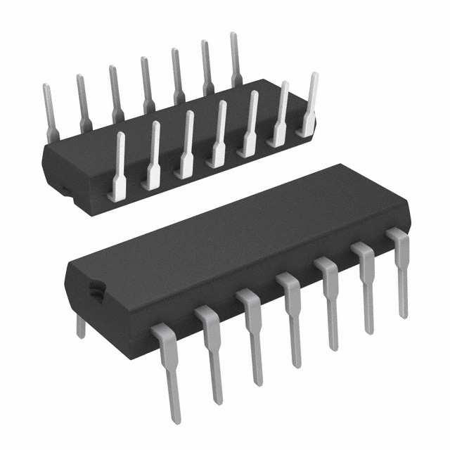
Connection Diagram
Dual-In-Line Package
Order Number MM54C914 or MM74C914
TL F 5917 – 1
Top View Special Input Protection
8V 25V for the diodes
TL F 5917 – 2
C1995 National Semiconductor Corporation
TL F 5917
RRD-B30M105 Printed in U S A
�Absolute Maximum Ratings
(Note 1) Storage Temperature Range (TS) Power Dissipation Dual-In-Line Small Outline Operating VCC Range Absolute Maximum (VCC) Lead Temperature (TL) (Soldering 10 seconds)
b 65 C to a 150 C
If Military Aerospace specified devices are required please contact the National Semiconductor Sales Office Distributors for availability and specifications VCC b 25V to GND a 25V b 0 3V to VCC a 0 3V Voltage at any other Pin Operating Temperature Range (TA) b 55 C to a 125 C MM54C914 b 40 C to a 85 C MM74C914 Voltage at any Input Pin
700 mW 500 mW 3V to 15V 18V 300 C
DC Electrical Characteristics Min
Symbol CMOS TO CMOS VT a Positive Going Threshold Voltage Parameter
Max limits apply across temperature range unless otherwise noted Conditions Min Typ Max Units
VCC e 5V VCC e 10V VCC e 15V VCC e 5V VCC e 10V VCC e 15V VCC e 5V VCC e 10V VCC e 15V VCC e 5V IO e b10 mA VCC e 10V IO e b10 mA VCC e 5V IO e a 10 mA VCC e 10V IO e a 10 mA VCC e 15V VIN e 25V VCC e 15V VIN e b10V VCC VCC VCC VCC
e e e e
30 60 90 07 14 21 10 20 30 45 90
36 68 10 14 32 5 22 36 5
43 86 12 9 20 40 60 36 72 10 8
V V V V V V V V V
VTb
Negative Going Threshold Voltage
VT a b VTb
Hysteresis
VOUT(1) VOUT(0) IIN(1) IIN(0) ICC
Logical ‘‘1’’ Output Voltage Logical ‘‘0’’ Output Voltage Logical ‘‘1’’ Input Current Logical ‘‘0’’ Input Current Supply Current
05 10 0 005
b 100 b 0 005
V V mA mA
50
15V VIN e b 10V 25V 5V VIN e b 2 5V (Note 4) 10V VIN e 5V (Note 4) 15V VIN e 7 5V (Note 4)
0 05 20 200 600
300
mA mA mA mA
CMOS LPTTL INTERFACE VIN(1) VIN(0) VOUT(1) VOUT(0) Logical ‘‘1’’ Input Voltage Logical ‘‘0’’ Input Voltage Logical ‘‘1’’ Output Voltage Logical ‘‘0’’ Output Voltage VCC e 5V VCC e 5V 54C VCC e 4 5V IO e b360 mA 74C VCC e 4 75V IO e b360 mA 54C VCC e 4 5V IO e 360 mA 74C VCC e 4 75V IO e 360 mA 24 24 04 04 43 07 V V V V V V
OUTPUT DRIVE (See 54C 74C Family Characteristics Data Sheet) (Short Circuit Current) ISOURCE ISOURCE ISINK ISINK Output Source Current (P-Channel) Output Source Current (P-Channel) Output Sink Current (N-Channel) Output Sink Current (N-Channel) VCC e 5V VOUT e 0V TA e 25 C VCC e 10V VOUT e 0V TA e 25 C VCC e 5V VOUT e VCC TA e 25 C VCC e 10V VOUT e VCC TA e 25 C
b 1 75 b8 0 b3 3 b 15
mA mA mA mA
1 75 80
36 16
2
�AC Electrical Characteristics
Symbol tPHL tPLH CIN CPD Parameter
TA e 25 C CL e 50 pF unless otherwise specified Conditions VCC e 5V VCC e 10V Min Typ 220 80 5 20 Max 400 200 Units ns ns pF pF
Propagation Delay from Input to Output
Input Capacitance Power Dissipation Capacitance
Any Input (Note 2) (Note 3) Per Gate
AC Parameters are guaranteed by DC correlated testing Note 1 ‘‘Absolute Maximum Ratings’’ are those values beyond which the safety of the device cannot be guaranteed Except for ‘‘Operating Temperature Range’’ they are not meant to imply that the devices should be operated at these limits The table of ‘‘Electrical Characteristics’’ provides conditions for actual device operation Note 2 Capacitance is guaranteed by periodic testing Note 3 CPD determines the no load AC power consumption of any CMOS device For complete explanation see 54C 74C Family Characteristics Application Note AN-90 Note 4 Only one input is at VCC the others are either at VCC or GND
Typical Performance Characteristics
Typical Transfer Characteristics Guaranteed Trip Point Range
TL F 5917 – 4
TL F 5917 – 5
Typical Application
TL F 5917 – 3
Note VCC1 e VCC2 GND1 e GND2
TL F 5917 – 6
3
�MM54C914 MM74C914 Hex Schmitt Trigger with Extended Input Voltage
Physical Dimensions inches (millimeters)
Ceramic Dual-In-Line Package (J) Order Number MM54C914J or MM74C914J NS Package Number J14A
Molded Dual-In-Line Package (N) Order Number MM54C914N or MM74C914N NS Package Number N14A LIFE SUPPORT POLICY NATIONAL’S PRODUCTS ARE NOT AUTHORIZED FOR USE AS CRITICAL COMPONENTS IN LIFE SUPPORT DEVICES OR SYSTEMS WITHOUT THE EXPRESS WRITTEN APPROVAL OF THE PRESIDENT OF NATIONAL SEMICONDUCTOR CORPORATION As used herein 1 Life support devices or systems are devices or systems which (a) are intended for surgical implant into the body or (b) support or sustain life and whose failure to perform when properly used in accordance with instructions for use provided in the labeling can be reasonably expected to result in a significant injury to the user
National Semiconductor Corporation 1111 West Bardin Road Arlington TX 76017 Tel 1(800) 272-9959 Fax 1(800) 737-7018
2 A critical component is any component of a life support device or system whose failure to perform can be reasonably expected to cause the failure of the life support device or system or to affect its safety or effectiveness
National Semiconductor Europe Fax (a49) 0-180-530 85 86 Email cnjwge tevm2 nsc com Deutsch Tel (a49) 0-180-530 85 85 English Tel (a49) 0-180-532 78 32 Fran ais Tel (a49) 0-180-532 93 58 Italiano Tel (a49) 0-180-534 16 80
National Semiconductor Hong Kong Ltd 13th Floor Straight Block Ocean Centre 5 Canton Rd Tsimshatsui Kowloon Hong Kong Tel (852) 2737-1600 Fax (852) 2736-9960
National Semiconductor Japan Ltd Tel 81-043-299-2309 Fax 81-043-299-2408
National does not assume any responsibility for use of any circuitry described no circuit patent licenses are implied and National reserves the right at any time without notice to change said circuitry and specifications
�
很抱歉,暂时无法提供与“MM74C914N”相匹配的价格&库存,您可以联系我们找货
免费人工找货