MM54HCT573 MM74HCT573 TRI-STATE Octal D-Type Latch MM54HCT574 MM74HCT574 TRI-STATE Octal D-Type Flip-Flop
PRELIMINARY
February 1990
MM54HCT573 MM74HCT573 TRI-STATE Octal D-Type Latch MM54HCT574 MM74HCT574 TRI-STATE Octal D-Type Flip-Flop
General Description
The MM54HCT573 MM74HCT573 octal D-type latches and MM54HCT574 MM74HCT574 Octal D-type flip flops advanced silicon-gate CMOS technology which provides the inherent benefits of low power consumption and wide power supply range but are LS-TTL input and output characteristic pin-out compatible The TRI-STATE outputs are capable of driving 15 LS-TTL loads All inputs are protected from damage due to static discharge by internal diodes to VCC and ground When the MM54HCT573 MM74HCT573 LATCH ENABLE input is high the Q outputs will follow the D inputs When the LATCH ENABLE goes low data at the D inputs will be retained at the outputs until LATCH ENABLE returns high again When a high logic level is applied to the OUTPUT CONTROL input all outputs go to a high impedance state regardless of what signals are present at the other inputs and the state of the storage elements The MM54HCT574 MM74HCT574 are positive edge triggered flip-flops Data at the D inputs meeting the setup and hold time requirements are transferred to the Q outputs on positive going transitions of the CLOCK (CK) input When a high logic level is applied to the OUTPUT CONTROL (OC) input all outputs go to a high impedance state regardless of what signals are present at the other inputs and the state of the storage elements MM54HCT MM74HCT devices are intended to interface between TTL and NMOS components and standard CMOS devices These parts are also plug in replacements for LSTTL devices and can be used to reduce power consumption in existing designs
Features
Y Y Y Y Y Y
TTL input characteristic compatible Typical propagation delay 18 ns Low input current 1 mA maximum Low quiescent current 80 mA maximum Compatible with bus-oriented systems Output drive capability 15 LS-TTL loads
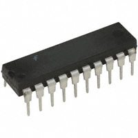
Connection Diagram
Dual-In-Line Package
TL F 10627 – 1
Top View Order Number MM54HCT573 or MM74HCT573
TL F 10627 – 2
Top View Order Number MM54HCT574 or MM74HCT574
Please look into Section 8 Appendix D for availability of various package types
TRI-STATE is a registered trademark of National Semiconductor Corporation C1995 National Semiconductor Corporation TL F 10627 RRD-B30M105 Printed in U S A
�Absolute Maximum Ratings (Notes 1
2)
Operating Conditions
Supply Voltage (VCC) DC Input or Output Voltage (VIN VOUT) Operating Temp Range (TA) MM74HCT MM54HCT Input Rise or Fall Times (tr tf) Min 45 0 Max 55 VCC Units V V
If Military Aerospace specified devices are required please contact the National Semiconductor Sales Office Distributors for availability and specifications
b 0 5 to a 7 0V Supply Voltage (VCC) b 1 5 to VCC a 1 5V DC Input Voltage (VIN) b 0 5 to VCC a 0 5V DC Output Voltage (VOUT) g 20 mA Clamp Diode Current (IIK IOK) g 35 mA DC Output Current per pin (IOUT) g 70 mA DC VCC or GND Current per pin (ICC) b 65 C to a 150 C Storage Temperature Range (TSTG) Power Dissipation (PD) (Note 3) 600 mW S O Package only 500 mW Lead Temp (TL) (Soldering 10 seconds) 260 C
b 40 b 55
a 85 a 125
C C ns
500
DC Electrical Characteristics VCC e 5V g 10% (unless otherwise specified)
Symbol Parameter Conditions TA e 25 C Typ VIH VIL VOH Minimum High Level Input Voltage Maximum Low Level Input Voltage Minimum High Level Output Voltage VIN e VIH or VIL lIOUTl e 20 mA lIOUTl e 6 0 mA VCC e 4 5V lIOUTl e 7 2 mA VCC e 5 5V VIN e VIH or VIL lIOUTl e 20 mA lIOUTl e 6 0 mA VCC e 4 5V lIOUTl e 7 2 mA VCC e 5 5V VIN e VCC or GND VIH or VIL VOUT e VCC or GND Enable e VIH or VIL VIN e VCC or GND IOUT e 0 mA VIN e 2 4V or 0 5V (Note 4)
Note 2 Unless otherwise specified all voltages are referenced to ground Note 3 Power Dissipation temperature derating plastic ‘‘N’’ package b 12 mW C from 65 C to 85 C ceramic ‘‘J’’ package b 12 mW C from 100 C to 125 C Note 4 Measured per pin All others tied to VCC or ground
74HCT TA eb40 to 85 C
54HCT TA eb55 to 125 C
Units
Guaranteed Limits 20 08 20 08 20 08 V V
VCC 42 57 0 02 02
VCCb0 1 3 98 4 98 01 0 26 0 26
g0 1
VCCb0 1 3 84 4 84 01 0 33 0 33
g1 0
VCCb0 1 37 47 01 04 04
g1 0
V V V V V V mA mA
VOL
Maximum Low Level Voltage
IIN IOZ
Maximum Input Current Maximum TRI-STATE Output Leakage Current Maximum Quiescent Supply Current
g0 5
g5 0
g 10
ICC
80 15
80 18
160 20
mA mA
Note 1 Absolute Maximum Ratings are those values beyond which damage to the device may occur
2
�AC Electrical Characteristics MM54HCT573 MM74HCT573 VCC e 5 0V tr e tf e 6 ns TA e 25 C (unless otherwise specified)
Symbol tPHL tPLH tPHL tPLH tPZH tPZL tPHZ tPLZ tW tS tH Parameter Maximum Propagation Delay Data to Output Maximum Propagation Delay Latch Enable to Output Maximum Enable Propagation Delay Control to Output Maximum Disable Propagation Delay Control to Output Minimum Clock Pulse Width Minimum Setup Time Data to Clock Minimum Hold Time Clock to Data Conditions CL e 45 pF CL e 45 pF CL e 45 pF RL e 1 kX CL e 5 pF RL e 1 kX Typ 17 16 21 14 Guaranteed Limit 27 27 30 23 15 5 12 Units ns ns ns ns ns ns ns
AC Electrical Characteristics MM54HCT573 MM74HCT573 VCC e 5 0V g 10% tr e tf e 6 ns (unless otherwise specified)
Symbol tPHL tPLH tPHL tPLH tPZH tPZL tPHZ tPLZ tTHL tTLH tW tS tH CIN COUT CPD Parameter Maximum Propagation Delay Data to Output Maximum Propagation Delay Latch Enable to Output Maximum Enable Propagation Delay Control to Output Maximum Disable Propagation Delay Control to Output Maximum Output Rise and Fall Time Minimum Clock Pulse Width Minimum Setup Time Data to Clock Minimum Hold Time Clock to Data Maximum Input Capacitance Maximum Output Capacitance Power Dissipation Capacitance (Note 5) OC e VCC OC e GND
b3
Conditions CL e 50 pF CL e 50 pF CL e 50 pF RL e 1 kX CL e 50 pF RL e 1 kX CL e 50 pF
TA e 25 C Typ 18 17 22 15 6 30 30 30 30 12 15 5 12 10 20 5 52 4
74HCT TA eb40 to 85 C
54HCT TA eb55 to 125 C
Units
Guaranteed Limits 38 44 38 38 15 20 6 15 10 20 45 53 45 45 18 24 8 18 10 20 ns ns ns ns ns ns ns ns pF pF pF pF
Note 5 CPD determines the no load dynamic power consumption PD e CPD VCC2 f a ICC VCC and the no load dynamic current consumption IS e CPD VCC f a ICC
Truth Table
’HCT573 Output Control L L L H LE H H L X Data H L X X Output H L Q0 Z Output Control L L L H
X e Don’t Care
’HCT574 Clock Data H L X X Output H L Q0 Z
u u
L X
H e high level L e low level Q0 e level of output before steady-state input conditions were established Z e high impedance
H e High Level L e Low Level
u e Transition from low-to-high
Z e High impedance state Q0 e The level of the output before steady state input conditions were established
3
�AC Electrical Characteristics MM54HCT574 MM74HCT574 VCC e 5 0V tr e tf e 6 ns TA e 25 C (unless otherwise specified)
Symbol fMAX tPHL tPLH tPZH tPZL tPHZ tPLZ tW tS tH Parameter Maximum Clock Frequency Maximum Propagation Delay to Output Maximum Enable Propagation Delay Control to Output Maximum Disable Propagation Delay Control to Output Minimum Clock Pulse Width Minimum Setup Time Data to Clock Minimum Hold Time Clock to Data CL e 45 pF CL e 45 pF RL e 1 kX CL e 5 pF RL e 1 kX Conditions Typ 60 17 19 14 Guaranteed Limit 33 27 28 25 15 12 5 Units MHz ns ns ns ns ns ns
AC Electrical Characteristics MM54HCT574 MM74HCT574 VCC e 5 0V g 10% tr e tf e 6 ns (unless otherwise specified)
Symbol Parameter Conditions TA e 25 C Typ fMAX Maximum Clock Frequency CL e 50 pF CL e 50 pF RL e 1 kX CL e 50 pF RL e 1 kX CL e 50 pF 18 22 15 6 33 30 30 30 12 15 6
b1
74HCT 54HCT TA eb40 to 85 C TA eb55 to 125 C Units Guaranteed Limits 28 38 38 38 15 20 15 6 10 20 23 45 45 45 18 24 18 8 10 20 MHz ns ns ns ns ns ns ns pF pF pF pF
tPHL tPLH Maximum Propagation Delay Clock to Output tPZH tPZL Maximum Enable Propagation Delay Control to Output tPHZ tPLZ Maximum Disable Propagation Delay Control to Output tTHL tTLH Maximum Output Rise and Fall Time tW tS tH CIN COUT CPD Minimum Clock Pulse Width Minimum Setup Time Data to Clock Minimum Hold Time Clock to Data Maximum Input Capacitance Maximum Output Capacitance
12 5 10 20 5 58
Power Dissipation Capacitance (Note 5) OC e VCC OC e GND
Note 5 CPD determines the no load power consumption PD e CPD VCC2 f a ICC VCC and the no load dynamic current consumption IS e CPD VCC f a ICC
4
�Physical Dimensions inches (millimeters)
Order Number MM74HCT573 HCT574 (WM) NS Package Number M20B
5
�MM54HCT573 MM74HCT573 TRI-STATE Octal D-Type Latch MM54HCT574 MM74HCT574 TRI-STATE Octal D-Type Flip-Flop
Physical Dimensions inches (millimeters) (Continued)
Lit
111670
Order Number MM74HCT573N HCT574 (N) NS Package Number N20A
LIFE SUPPORT POLICY NATIONAL’S PRODUCTS ARE NOT AUTHORIZED FOR USE AS CRITICAL COMPONENTS IN LIFE SUPPORT DEVICES OR SYSTEMS WITHOUT THE EXPRESS WRITTEN APPROVAL OF THE PRESIDENT OF NATIONAL SEMICONDUCTOR CORPORATION As used herein 1 Life support devices or systems are devices or systems which (a) are intended for surgical implant into the body or (b) support or sustain life and whose failure to perform when properly used in accordance with instructions for use provided in the labeling can be reasonably expected to result in a significant injury to the user
National Semiconductor Corporation 1111 West Bardin Road Arlington TX 76017 Tel 1(800) 272-9959 Fax 1(800) 737-7018
2 A critical component is any component of a life support device or system whose failure to perform can be reasonably expected to cause the failure of the life support device or system or to affect its safety or effectiveness
National Semiconductor Europe Fax (a49) 0-180-530 85 86 Email cnjwge tevm2 nsc com Deutsch Tel (a49) 0-180-530 85 85 English Tel (a49) 0-180-532 78 32 Fran ais Tel (a49) 0-180-532 93 58 Italiano Tel (a49) 0-180-534 16 80
National Semiconductor Hong Kong Ltd 13th Floor Straight Block Ocean Centre 5 Canton Rd Tsimshatsui Kowloon Hong Kong Tel (852) 2737-1600 Fax (852) 2736-9960
National Semiconductor Japan Ltd Tel 81-043-299-2309 Fax 81-043-299-2408
National does not assume any responsibility for use of any circuitry described no circuit patent licenses are implied and National reserves the right at any time without notice to change said circuitry and specifications
�
很抱歉,暂时无法提供与“MM74HCT573N”相匹配的价格&库存,您可以联系我们找货
免费人工找货